注:该论文发表于 2003 年第九届国际异步电路与系统研讨会(ASYNC 2003),围绕触发器、同步链路、异步握手电路等基础数字单元,研究异步时钟域同步器设计、亚稳态规避、握手协议、复位同步、可测试性(DFT)等底层技术,所阐述的跨时钟域与异步同步设计理论,通用于 FPGA、ASIC、SoC、GALS 等各类多时钟数字硬件平台。
英文引文,机翻未校。
如有内容异常,请看原文。
Fourteen Ways to Fool Your Synchronizer
十四种同步器设计误区
Ran Ginosar
VLSI Systems Research Center, Technion-Israel Institute of Technology Haifa 32000, Israel
ran@ee.technion.ac.il
兰·吉诺萨尔
以色列理工学院 超大规模集成电路系统研究中心,海法 32000,以色列
邮箱:ran@ee.technion.ac.il
Abstract
摘要
Transferring data between mutually asynchronous clock domains requires safe synchronization. However, the exact nature of synchronization sometimes eludes designers, and as a result synchronization circuits get "optimized" to the point where they do no longer operate correctly. This paper reviews a number of such cases, analyzes the causes of the errors, and offers a correct synchronizer circuit for each case. A correct two-flop synchronizer is presented. After discussing cases that avoid synchronization, the following synchronizers are reviewed: one flop, sneaky path, greedy path, wrong protocol, global reset, async clear, DFT leakage, pulse, slow-to-fast, metastability blocker, parallel and shared flop synchronizers.
异步时钟域之间的数据传输必须依靠可靠的同步电路实现。但设计人员往往未能透彻理解同步电路的工作原理,对同步电路进行不当"优化",最终导致电路功能失效。本文梳理了各类典型错误设计案例,分析故障成因,并针对每类案例给出正确的同步电路方案。文中首先介绍标准的两级触发器同步器;在分析省略同步电路的错误设计后,依次剖析单触发器同步器、隐蔽路径同步器、激进路径同步器、协议错误型同步器、全局复位同步器、异步清零同步器、可测试性设计泄露问题、脉冲同步器、慢时钟转快时钟同步器、亚稳态阻断电路、并行同步器以及共享触发器同步器等十余类错误设计。
1. Introduction
1. 引言
Transferring data between mutually asynchronous clock domains requires safe synchronization 1-6. The operation of synchronization circuits has been recognized for a long time as being delicate and easy to disturb 1-3, 7-12, but at the same time robust synchronizer design does guarantee safe operation for all practical purposes. However, the exact nature of synchronization sometimes eludes designers, and as a result synchronization circuits get "optimized" to the point where they do no longer operate correctly. This paper reviews a number of such cases, analyzes the causes of the errors, and offers a correct synchronizer circuit for each case. The author has encountered those interesting cases while teaching, while working with various SOC (System on Chip) design teams, and while reviewing certain papers submitted for publication.
异步时钟域间的数据传输离不开可靠的同步机制1-6。业界早已公认,同步电路结构精密、极易因设计改动出现异常1-3, 7-12,但合理设计的同步器能够保证电路在实际应用中稳定工作。部分设计人员对同步电路的核心原理理解不足,盲目对其进行"优化",致使同步电路功能异常。本文整理了多类典型错误案例,分析故障根源,并逐一给出对应的正确同步电路方案。这些案例均来自笔者的教学工作、片上系统设计团队合作经历以及学术论文审稿过程。
The paper starts by presenting a (hopefully) correct two-flop synchronizer. Validation means and tools are discussed. Section 3 describes the various synchronizers, analyzes the errors and pitfalls, and offers suggestions.
本文首先介绍标准两级触发器同步器,并讲解对应的验证方法与工具;第 3 部分分类介绍各类同步器错误设计,分析缺陷与隐患并给出改进建议。
This paper focuses on the most general synchronization of two mutually-asynchronous clock domains. More aggressive synchronization circuits, which achieve high throughput data transfer between clock domains having the same or related frequencies, are not discussed here.
本文仅针对两个独立异步时钟域的通用同步场景展开论述,不探讨适用于同频/相关频时钟域、可实现高吞吐传输的特殊同步电路。
2. A Correct Two Flop Synchronizer
2. 标准两级触发器同步器
The simplest and safest method for the transfer of data between two mutually-asynchronous clock domains requires a two-flop synchronizer 2-4. A "push" synchronizer is shown in Figure 1, but the principles apply also to pull, push-pull, and control-only synchronizers.
实现异步时钟域数据传输,最简单且最可靠的方案是采用两级触发器同步器2-4。图 1 为推挽式同步器,其设计原理同样适用于拉取式、推拉结合式以及纯控制信号同步器。
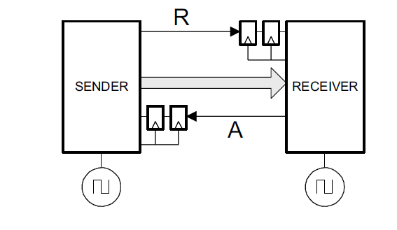
Figure 1: A push synchronizer
图 1:推挽式同步器
Bundled data is employed. The "synchronizer" actually comprises two synchronization circuits that envelope the data lines, implementing a complete handshake protocol. The Request ® and Acknowledge (A) lines are synchronized by the receiver and sender, respectively. The settling window T (namely the time separation between the two clock inputs to the two flops of the synchronizers) could be a whole clock cycle or a fraction thereof, and could be different for each side, as long as the desired reliability is obtained. Synchronizer reliability is typically expressed in terms of Mean Time Between Failures 2:
电路采用捆绑式数据传输方案。整套同步架构包含两组同步电路,围绕数据线构建完整的握手协议。请求信号(R)由接收端完成同步,应答信号(A)由发送端完成同步。稳定窗口 T T T 指同步器两级触发器时钟信号的时间间隔,该时长可以为一个完整时钟周期,也可以是部分时钟周期;收发两端的稳定窗口时长可不同,只需满足可靠性要求即可。同步器的可靠性通常用平均无故障时间(MTBF)表征2:
M T B F = e T / τ T W f A f D MTBF=\frac{e^{T / \tau}}{T_{W} f_{A} f_{D}} MTBF=TWfAfDeT/τ
where τ is the settling time constant of the flop, T W T_{W} TW a parameter related to its time window of susceptibility, f A f_{A} fA the synchronizer's clock frequency (the receiver's clock frequency for the R synchronizer and the sender's for the A synchronizer), and f D f_{D} fD is the frequency of pushing data across the clock domain boundary. Typically, MTBF is designed to be at least ten times the expected life of the product. If latency is not an issue, T is simply set to be a whole clock cycle, and for most SOCs it implies MTBF of many eons.
式中: τ \tau τ 为触发器的稳定时间常数, T W T_{W} TW 为触发器敏感窗口相关参数, f A f_{A} fA 为同步器时钟频率(请求信号同步器使用接收端时钟,应答信号同步器使用发送端时钟), f D f_{D} fD 为跨时钟域的数据传输频率。工程设计中,通常要求同步器平均无故障时间不低于产品预期使用寿命的 10 倍。若对传输延迟无严格要求,可将稳定窗口 T T T 设为一个完整时钟周期,绝大多数片上系统采用该配置时,平均无故障时间可达亿万年之久。
The two synchronizers connect two simple finite state machines that implement the required protocol. A fourphase protocol is specified by means of a generalized STG in Figure 2, where "DD" means that the data is available (at the sender), "UU" means that it may be removed, and "LL" means data latched by the receiver. (A two-phase protocol may also be employed; the circuits are a bit more complex 13, 14, and this is typically used in order to minimize latency on long lines.) The complete logic and FSM are shown in Figure 3. A send request (V, true for a single cycle) latches data into (REG{S}) and starts the sender's FSM. The synchronized request (R2) latches the data into (REG{R}) and triggers the receiver's FSM. The receiver is given a single-cycle "data received" (D) signal. The protocol is sometimes modified so that A is set as soon as the received data are latched, but removed only after the receiver has had an opportunity to use the data.
两组同步电路分别对接简易有限状态机,共同实现握手协议。图 2 采用通用信号转移图描述四相位握手协议:DD 代表发送端数据就绪,UU 代表数据可移除,LL 代表接收端已锁存数据。电路也可采用二相位协议,但其结构相对复杂13,14,一般用于长线传输场景以降低延迟。完整逻辑电路与有限状态机如图 3 所示。发送请求信号 V(高电平持续一个时钟周期)将数据锁存至发送端寄存器 (REG{S}),并启动发送端状态机;经过同步后的请求信号 R2 将数据锁存至接收端寄存器 (REG{R}),同时触发接收端状态机,并产生一个时钟周期宽度的数据接收信号 D。该协议也可做变体设计:接收端锁存数据后立即置位应答信号 A,待接收端完成数据处理后再清除 A 信号。
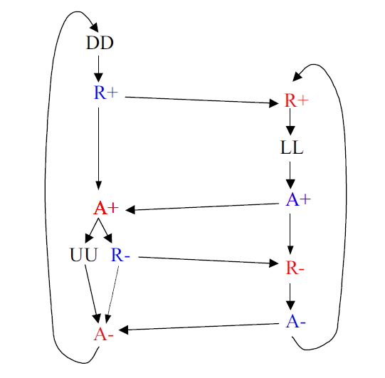
Figure 2: Four-phase handshake push synchronization protocol STG
图 2:推挽式同步器四相位握手协议信号转移图
DD(数据就绪)
R+(请求置位)
R+(请求置位)
LL(数据锁存)
A+(应答置位) A+(应答置位)
A+(应答置位) A+(应答置位)
UU(数据可移除) R-(请求复位)
R-(请求复位)
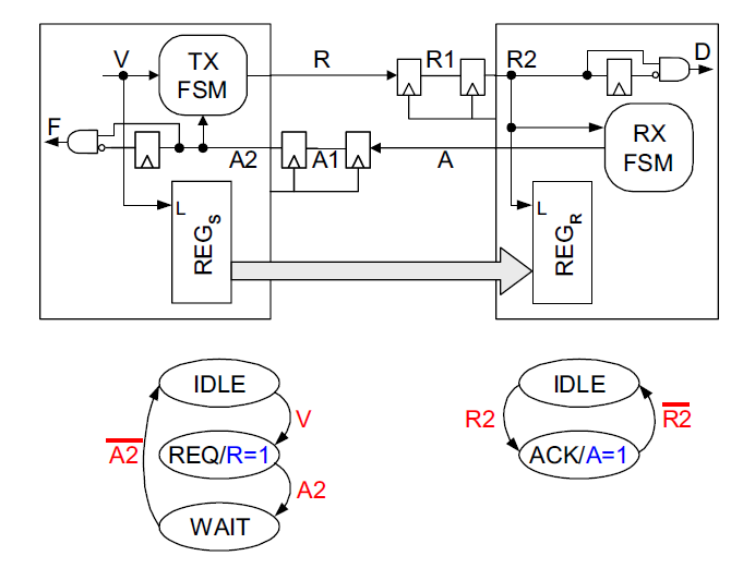
Figure 3: Push synchronizer logic and protocol FSM
图 3:推挽式同步器逻辑电路与协议有限状态机
发送端有限状态机 TX R2
接收端有限状态机 RX
发送端寄存器 REGS
接收端寄存器 REGR
空闲态 IDLE
请求态 REQ / R=1
应答态 ACK / A=1
等待态 WAIT
To consider the synchronizer's behavior in cases of conflicts, assume that T equals a whole clock cycle. Upon a potential clock-data conflict on R, one of three possible outcomes may happen (Figure 4):
假设稳定窗口 (T) 为一个完整时钟周期,分析时钟与数据冲突场景下同步器的工作状态。当请求信号 R 出现时钟与数据冲突时,会产生以下三种结果(图 4):
a. The rising edge of R is sampled high. R2 goes high on cycle 2, and data is latched into (REG{R}) by the beginning of cycle 3.
时钟采样到 R 的上升沿,判定信号为高电平。R2 在第 2 个时钟周期置高,数据在第 3 个时钟周期起始时刻被锁存至接收端寄存器 (REG{R})。
b. The rising edge of R is sampled low. Since the protocol assures that R stays high as long is A is low, it will be sampled high on cycle 2, when it is surely stable high. R2 will go high on cycle 3, and data is latched into (REG{R}) by cycle 4.
时钟采样 R 上升沿时判定信号为低电平。根据握手协议,应答信号 A 为低电平时 R 会持续保持高电平,因此第 2 个时钟周期会采样到稳定的高电平。R2 在第 3 个时钟周期置高,数据在第 4 个时钟周期被锁存至 (REG{R})。
c. The first flop goes metastable. With a probability of (1-e^{-T / \tau}) (which is infinitesimally close to 1), the flop has exited metastability by the next clock, and has arbitrarily settled to either high or low (the thick traces of R1 in the figure). If high, then R2 goes high on cycle 2. If low, it will surely go high on the next cycle, when the input R is already stable high, and R2 goes high on cycle 3.
第一级触发器进入亚稳态。触发器在下一个时钟沿到来前退出亚稳态的概率为 (1-e^{-T / \tau})(该概率无限趋近于 1),最终随机稳定在高电平或低电平(对应图中 R1 粗线波形)。若稳定为高电平,R2 在第 2 周期置高;若稳定为低电平,下一个周期输入 R 已稳定为高电平,必然会被采样到,R2 在第 3 周期置高。
A word of caution is due here: Although outcome c above implies that metastability typically disappears within a single clock cycle, the second flop is still required. An exception is discussed in Section 3.2 below.
此处需要特别说明:即便上述场景表明亚稳态通常会在一个时钟周期内消退,第二级触发器依然不可或缺。唯一特例将在下文 3.2 节中讨论。
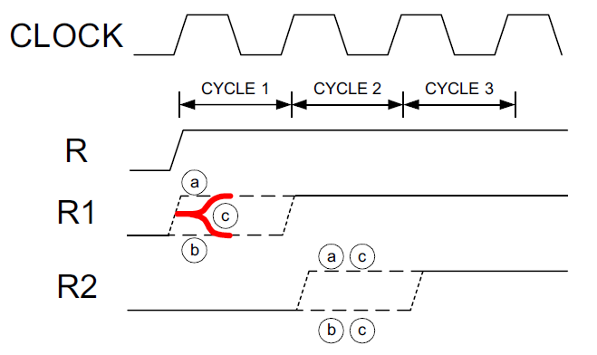
Figure 4: Three synchronization scenarios
时钟
图 4:三种同步工作场景
第 1 周期 第 2 周期 第 3 周期
A VHDL specification of the synchronizer is shown in Figure 5. This is a highly sensitive code, where minor modifications may render the synchronizer useless. Some such innovative but often fatal modifications are reviewed in the rest of this paper.
该同步器的 VHDL 代码如图 5 所示。同步电路代码容错性极低,微小改动都可能导致同步功能失效。本文后续章节将分析各类看似优化、实则致命的代码与电路改动方案。
Logic validation tools are typically incapable of detecting any errors in such synchronizers. When reasonable logic assumptions are made, many erroneous synchronizers appear to operate perfectly well. Synchronizer-specific verification algorithms are required for this analysis.
常规逻辑验证工具无法检测同步器的隐性故障。在仿真逻辑约束下,大量错误设计的同步器会表现出正常工作状态,因此必须采用同步电路专用的验证算法完成检测。
vhdl
-- TRANSMITTER (inputs V, A, output R)
if rising_edge(tx_clock) then
    A2 <= A1;
    A1 <= A;          -- 2 flop synchronizer
    A3 <= A2;
    F  <= not A3 and A2;  -- 1 shot pulse generator

    case (tx_fsm_state) is
        when idle =>
            if (V = '1') then
                tx_fsm_state <= req;
            end if;
            R <= '1';

        when req =>
            if (A2 = '1') then
                tx_fsm_state <= waiting;
                R <= '0';
            end if;

        when waiting =>
            if (A2 = '0') then
                tx_fsm_state <= idle;
            end if;

        when others =>
            tx_fsm_state <= idle;
            R <= '0';
    end case;
end if;

-- RECEIVER (input R, output A)
if rising_edge(rx_clock) then
    R2 <= R1;
    R1 <= R;          -- 2 flop synchronizer
    R3 <= R2;
    D  <= not R3 and R2;  -- 1 shot pulse generator

    case (rx_fsm_state) is
        when idle =>
            if (R2 = '1') then
                rx_fsm_state <= ack;
            end if;
            A <= '1';

        when ack =>
            if (R2 = '0') then
                rx_fsm_state <= idle;
            end if;
            A <= '0';

        when others =>
            rx_fsm_state <= idle;
            A <= '0';
    end case;
end if;
Figure 5: Push 2-way 4-phase synchronizer VHDL specification
图 5:双向推挽式四相位同步器 VHDL 代码
One tool has been developed specifically for validating synchronization. The Avant! Clock Domain Checker 15 is a decent first attempt at addressing this issue. However, it has a number of drawbacks: First, the control and data signals that cross domain boundaries must be named in a manner that facilitates these checks. Second, it validates only one-sided transfers and does not examine complete two-sided protocols and the protocol state machines. Third, it only validates a limited set of pre-defined rules, mostly covering a simple two-flop synchronizer and data lines protected by it; for instance, it does not check the synchronization of asynchronous reset. Fourth, it only handles "push" (and control-only) synchronizers, but neither "pull" nor "push-pull" ones. Another such tool is @Verifier from @HDL 16.
目前已有专用同步电路验证工具。Avant! 时钟域检查工具15是较早的同步验证工具,但存在诸多缺陷:第一,跨时钟域的控制、数据信号必须按照规范命名,工具才能完成检测;第二,仅支持单向数据传输验证,无法校验完整的双向握手协议与状态机;第三,仅能依据预设规则做检测,规则主要覆盖基础两级触发器同步器及受其保护的数据线,无法校验异步复位等信号的同步设计;第四,仅支持推挽式同步器与纯控制信号同步器,不兼容拉取式、推拉结合式同步器。另一款同类工具为 @HDL 公司的 @Verifier16。
3. The Interesting Synchronizers
3. 各类典型错误同步器设计
3.1 Avoiding the Synchronizer
3.1 省略同步电路
The most common synchronization error is the transfer of a signal from one clock domain into another without any synchronization. In some cases the designer felt that failure probability was too low to worry about (he has learned about MTBF in the range of (100) years, so why bother?). In other cases, the receiver operated at a much higher clock frequency than the sender, and the designer felt that the receiver would always be fast enough to catch the signal.
最常见的同步设计错误:跨时钟域信号传输完全省略同步电路。部分设计人员认为故障概率极低(已知平均无故障时间可达 100 年),无需额外做同步处理;还有一种误区是,当接收端时钟频率远高于发送端时,想当然认为接收端一定能采样到信号。
The incoming data is used as a combinational input to a combinational circuit, which eventually feeds into a flipflop. Since the timing of the input is unknown, there is no way to guarantee the timing of the output of the combinational circuit. In particular, it may change simultaneously with the sampling edge of the clock, and the receiving flip-flop may enter metastability or take excessively long time to respond, hampering correct operation of the next stage of logic 2.
跨域信号直接接入组合逻辑电路,最终送入触发器。由于输入信号时序不确定,组合逻辑输出时序也无法保证。若信号跳变与时钟采样沿同时发生,接收端触发器会进入亚稳态,或输出延迟大幅增加,导致后级逻辑工作异常2。
How often does the receiving flop enter metastability? The rate of entering metastability is (T{W} ×f{D} ×f{C}) . For a 0.18µm SOC (where (T{w} ≈50 ps) ) with a clock domain operating at 200MHz and receiving data every 1000 cycles, that rate is 2000/sec, namely two metastability events every millisecond. Ignoring such a high rate does take some courage!
触发器出现亚稳态的频次计算公式为:(T{W} ×f{D} ×f{C})。以 0.18 μm 工艺片上系统为例,其触发器敏感窗口 (T{W}≈50\ \text{ps}),时钟频率 200 MHz,每 1000 个时钟周期传输一次数据,计算可得亚稳态发生频次为 2000 次/秒,即每毫秒出现两次亚稳态。如此高的故障频次,完全忽视风险存在极大隐患。
This error can sometimes evade detection by normal logic validation tools. Simulations may assume such timing relations among the different clocks that all timing constraints are met. Static timing analysis would generate setup and hold violation warnings for every signal that crosses domain boundaries, but due to the typically huge number of such warnings most designers treat them as chaff and ignore them, assuming that the synchronizers will handle all those issues anyway. Consequently, legitimate warnings can easily be overlooked.
该类错误往往会躲过常规逻辑工具检测:仿真工具会默认不同时钟满足时序约束,无法发现问题;静态时序分析会针对所有跨时钟域信号报建立/保持时间违例,但这类告警数量庞大,多数设计人员会将其当作无效告警直接忽略,认为同步电路可解决所有问题,进而漏掉真实故障。
The error can be detected by the following clock domain crossing analysis, which can be performed using standard path analysis, e.g. as offered by logic synthesizers and by static timing analyzers. All possible pairs of clocks must be identified. For each pair, the CAD tool is made to report all logic paths that begin in a flop driven by the first clock and end in a flop driven by the second clock. The resulting list should be studied, either manually or with automated script, and every reported path must be approved. Typically, the crossing lists are carefully maintained and are used as 'false-path' specifications, instructing the analysis tool to ignore crossdomain paths that are already verified.
可通过跨时钟域路径分析排查该错误,逻辑综合工具、静态时序分析工具均支持标准路径分析功能。首先识别芯片内所有时钟配对组合,针对每一组时钟,让工具输出所有"起始触发器由第一个时钟驱动、终止触发器由第二个时钟驱动"的逻辑路径。设计人员需人工或通过脚本逐一核对路径,确认每一条跨域路径均做了合规同步处理。工程中会维护跨时钟域路径清单,并将已验证合规的路径设置为伪路径,让分析工具不再重复告警。
3.2 One Flop Synchronizer
3.2 单触发器同步器
A deceptively effective means of cutting down on the two-flop synchronizer's latency is to remove one of the flops (Figure 6).
为降低两级触发器同步器的传输延迟,部分设计人员会删减一级触发器,改为单触发器同步器(图 6),该方案看似可行,实则存在缺陷。
Figure 6: One-flop "synchronizer"
图 6:单触发器"同步器"
The problem comes about, of course, when there is a clock-data conflict. As explained above, the synchronizing flop may take an excessively long time to respond 2. Its output may be used in a standard combinational logic stage (the cloud in the figure), whose nominal propagation delay is typically close to a whole clock cycle. When the synchronizing flop fails (responding slowly), the input to the next flop will not be ready in time for the next clock cycle.
该电路的隐患出现在时钟与数据冲突场景:同步触发器的输出延迟会大幅增加2。触发器后级接有组合逻辑(图中云形模块),组合逻辑标准传输延迟接近一个时钟周期。一旦同步触发器响应延迟变长,下一级触发器就无法在时钟沿到来前采集到稳定数据。
The one-flop synchronizer can be detected by extending the analysis described above. The added step should validate that the output of every synchronizing flop feeds directly into the input of exactly one flop (driven by the same clock), without any logic in between.
可基于前文的跨时钟域路径分析做扩展,检测单触发器同步器:额外增加校验规则,要求所有同步触发器的输出必须直接接入同时钟域的下一级触发器,中间不得插入任何组合逻辑。
The one-flop synchronizer is acceptable when designed correctly. If the delay through the combinational 'cloud' in Figure 6 is (d,) the settling time is (T-d.) If that time is sufficient to assure the required MTBF, then this synchronizer is legal.
单触发器同步器并非绝对不可使用,需满足严格条件:设图中组合逻辑延迟为 (d),则有效稳定时间为 (T-d)。若该时长足以满足设计要求的平均无故障时间,单触发器同步器才可合规使用。
3.3 Sneaky Path
3.3 隐蔽跨域路径
Occasionally, a signal sneaks through a clock domain boundary unintentionally and unsynchronized. For instance, a signal has been moved from one clock domain to another as part of redesign, and some uses of the signal in its old domain are overlooked. It has also happened when a designer was unaware that a specific signal belonged to a different clock domain. In yet other cases, a signal S from a different clock domain is synchronized and renamed S _sync, but the designer has used S rather than S_sync by mistake.
电路改版过程中,常会出现信号未经同步、意外跨时钟域传输的隐蔽路径。例如:改版设计将信号迁移至新时钟域,但该信号在原时钟域的部分引用端口未清理;设计人员不了解信号所属时钟域,直接跨域调用;跨域信号 S 完成同步后重命名为 S_sync,但代码中误使用原始信号 S 而非同步后的 S_sync。
The situation is similar to case 3.1 above, and so are the solutions.
该类问题的故障原理与解决方法和 3.1 节省略同步电路的场景完全一致。
3.4 Greedy Path Synchronizer
3.4 激进路径同步器
The designer employed a good two-flop synchronizer, but decided to save a little latency with the arrival detector: (D=R1 ×\overline{R2}) (Figure 7). This is quite similar to the one-flop synchronizer: The problem is that D is used with additional combinational logic, and the timing of that combinational path is typically designed to fit within a single clock cycle. But in cases of clock-data conflict of R, R1 may take longer than the normal flop tPD to stabilize, and consequently the entire combinational path from R1 through D and to the last flop fails to converge during a single cycle. The right solution, obviously, is to add a flop and set (D=R2 ×\overline{R3}) (as in Figure 3).
设计人员使用了标准两级触发器同步器,但为进一步降低延迟,将数据接收检测逻辑改为 (D=R1 ×\overline{R2})(图 7)。该缺陷与单触发器同步器类似:检测信号 D 会接入额外组合逻辑,而组合逻辑路径的时序裕量仅设计为一个时钟周期。当请求信号 R 发生时钟数据冲突时,R1 的稳定时间会超出触发器标准传输延迟,导致从 R1 经 D 到末级触发器的整条组合路径,无法在一个时钟周期内完成信号稳定。正确方案是增加一级触发器,采用 (D=R2 ×\overline{R3}) 逻辑(如图 3 所示)。
Figure 7: Greedy path "synchronizer"
图 7:激进路径"同步器"
3.5 Wrong Protocol
3.5 握手协议错误
Consider the following example. The sender in a push synchronizer is a CPU that can be tuned to operate in the range of 60-100 MHz. The receiver is a communication modem based on a 55MHz clock. A push synchronizer is used to transfer data from the CPU to the modem. The designer has correctly realized that, once R is set, it would take at most four cycles of the receiver's clock to latch the data into (REG_{R}) (as in Figure 4). Based on the relative speeds, this would mean up to eight cycles of the faster sender's clock. To save time and logic, the designer eliminated the A line and its synchronizer; instead, he inserted a nine-cycle delay in the sender's FSM. After the delay, R is reset and the transfer is assumed finished.
举例说明:推挽式同步器的发送端为主频 60~100 MHz 的中央处理器,接收端为时钟 55 MHz 的通信调制解调器,用于处理器向调制解调器传输数据。设计人员判断,请求信号 R 置位后,接收端最多耗时 4 个自身时钟周期即可锁存数据(参考图 4);按照时钟速率换算,对应发送端最多 8 个时钟周期。为简化电路、降低延迟,设计人员删除应答信号线 A 及其同步电路,转而在发送端状态机中增加 9 个时钟周期的延时,延时结束后直接复位 R 信号,判定数据传输完成。
There were two problems with that novel design. First, the designer did not realize that he had violated the safety (or 1-boundedness) requirement of the protocol (namely, transitions must be acknowledged, or else an STG arc might accumulate multiple tokens 17, 18). Although the data was safely latched into (REG_{R}) , at times the receiver was busy doing something else and did not manage to make use of the data before a new set of data has arrived, over-writing the old.
该改版设计存在两处严重问题:第一,违背握手协议的安全约束(单令牌约束),信号状态切换必须配合应答机制,否则信号转移图链路会出现令牌堆积问题17,18。即便数据正常锁存至接收端寄存器,若接收端忙于其他任务,尚未处理当前数据时新数据就已到达,旧数据会被直接覆盖。
Second, while the modem remained at 55MHz, the CPU in a later chip generation was sped up to 200MHz. At that rate, nine sender's clock cycles weren't enough any more to cover four modem cycles, and the synchronizer broke down.
第二,后续芯片迭代中,调制解调器时钟仍为 55 MHz,但处理器主频升级至 200 MHz。此时发送端 9 个时钟周期,已无法覆盖接收端 4 个时钟周期的处理时长,同步电路彻底失效。
There are other ways by which the protocol can be violated. A powerful protocol verification algorithm might provide a useful tool to weed out such innovations.
握手协议还存在其他各类违规设计。可采用专业协议验证算法,排查这类私自修改协议的错误设计。
3.6 Global Reset Synchronizer
3.6 全局复位同步器
In a multi-frequency GALS (Globally Asynchronous, Locally Synchronous) SOC, a global reset signal is naturally asynchronous to at least some of the clock domains. The leading edge of the reset signal is harmless, as it forces all circuits to a known starting state. The trailing edge, on the other hand, is the culprit in some chips. During global reset all the various clocks are started and all PLLs settle into their respective different frequencies. When the reset is removed, it can happen simultaneously with the sampling edge of one of the clocks. The global reset is typically connected into the asynchronous clear (or preset) input of many flip-flops, and its trailing edge must respect a setup constraint, or else the flops may enter metastability.
在多时钟域的全局异步局部同步(GALS)片上系统中,全局复位信号必然与部分时钟域异步。复位信号的上升沿无安全隐患,可将所有电路强制置为初始状态;但下降沿是故障高发点。全局复位期间,各时钟电路启动、锁相环稳定至各自工作频率。当复位撤销时,其下降沿可能与某一时钟的采样沿同时到来。全局复位通常接入大量触发器的异步清零/置位端,因此复位信号下降沿必须满足建立时间约束,否则触发器会进入亚稳态。
A safe interface is shown in Figure 8. It belongs with each of the several clock generators of the SOC. While the leading edge is transferred without delay (when the clocks may be inoperative), the trailing edge is synchronized.
安全的全局复位接口如图 8 所示,该电路需配置在片上系统每一路时钟发生器处。复位上升沿直接传输(此时时钟电路通常未工作),下降沿则经过同步处理。
Figure 8: Global reset synchronizer
图 8:全局复位同步电路
RESET
RESET WITH SYNCHRONIZED TRAILING EDGE
CLOCK
复位信号
下降沿同步后的复位信号
时钟
3.7 Async Clear Synchronizer
3.7 异步清零同步器
Occasionally (and contrary to the wisdom of typical synchronous design methodologies) asynchronous clear or preset of a flop may be employed as part of the logic (rather than for global reset, as discussed in Section 3.6). Some designers feel that, since this is an asynchronous clear, it needs not be synchronized even when it crosses clock domain boundaries (Figure 9).
部分电路会使用触发器的异步清零/置位端实现逻辑功能(区别于 3.6 节的全局复位场景),该用法与标准同步设计理念相悖。部分设计人员认为,既然是异步清零信号,即便跨时钟域传输也无需做同步处理(图 9)。
Figure 9: Asynchronous clear
图 9:异步清零信号跨域传输
RESET
复位信号
The problem is very similar to that described in Section 3.6: Removal of the asynchronous clear signal may concur with the rising edge of the receiver's clock, potentially leading to metastability. The solution is either to synchronize the reset signal with two flops, or (when the leading edge must not be delayed) design an asymmetric synchronizer as in Figure 10.
该问题与 3.6 节全局复位场景原理一致:异步清零信号撤销(信号跳变)若与接收端时钟上升沿同时发生,会引发亚稳态。解决方案有两种:一是采用两级触发器对清零信号做同步;二是若要求信号上升沿无延迟,可采用图 10 所示的非对称同步电路。
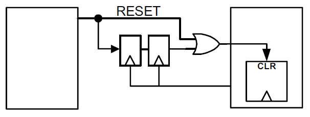
Figure 10: Synchronized-trail clear
图 10:下降沿同步的异步清零电路
RESET
复位信号
3.8 DFT Leakage
3.8 可测试性设计(DFT)路径泄露
Simple production testers may have only a single clock. To test a GALS SOC on such testers, all clocks are shorted together. Static faults (such as stuck-at) and some dynamic faults (speed testing of the individual clock domains) are properly tested that way. The clock shorts of course must be ignored during path analysis (by means of manually assembled 'false-path' lists or by instructing the analysis to ignore all paths that are conditioned upon a test-enable signal). But certain changes of the design may result in an error (sneaky) path masked by the list.
部分基础量产测试仪仅支持单时钟输入。为在这类设备上测试全局异步局部同步片上系统,会将芯片内所有时钟短接。该方式可完成固定型静态故障、单时钟域速率类动态故障的测试。在路径分析时,需要通过手动配置伪路径清单、屏蔽测试使能相关路径等方式,忽略时钟短接带来的无效路径。但电路改版后,部分隐蔽的跨域错误路径会被伪路径清单屏蔽,无法被检测。
The solution is to recheck the entire false-path list as a final check, after all design changes are completed.
解决方案:每次电路改版完成后,重新全面核对伪路径清单,作为最终校验环节。
3.9 Pulse Synchronizer
3.9 脉冲同步器
The pulse synchronizer (Figure 11) is designed to pass a single "pulse" (a logic signal that is set to '1' for only a single clock cycle) from one clock domain to another. A pulse on P causes the sender's flop to toggle. Eventually, D is set high for a single cycle of the receiver's clock as a result.
脉冲同步器(图 11)用于将单时钟周期宽度的脉冲信号跨时钟域传输。输入脉冲 P 会触发发送端触发器状态翻转,最终在接收端产生一个时钟周期宽度的输出脉冲 D。
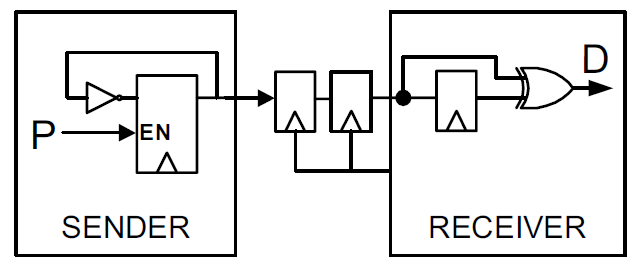
Figure 11: Pulse "synchronizer"
图 11:脉冲"同步器"
P EN
SENDER RECEIVER
P 使能信号 EN
发送端 接收端
The designer was lucky to discover the problem when the circuit was tried on an FPGA, prior to tapeout. Sometimes the P input was set to '1' for two consecutive cycles. At other times two pulses came in succession, with only one cycle in between. In both cases the synchronizer has generated undesirable results. The astute reader can easily figure out what they were. The situation was mended by replacing this with a standard control-only synchronizer, operating with a standard two-phase protocol.
该电路的缺陷在芯片流片前的现场可编程门阵列测试中被发现:当输入脉冲 P 连续两个周期为高电平,或两个脉冲间隔仅一个时钟周期时,该同步器都会输出异常。读者可自行推导具体故障现象。整改方案为:替换为标准纯控制信号同步器,采用二相位握手协议实现脉冲跨域传输。
3.10 Slow-to-Fast Synchronizer
3.10 慢时钟转快时钟同步器
When the sender uses a slower clock than the receiver, designers can simplify the handshake protocol: The R line, when set for a single cycle of the sender's clock, is sampled by at least two edges of the receiver's clock. If the first edge misses, the second one is guaranteed to sample R. If the first one succeeds, further sampling is blocked (Figure 12), so that metastability during the second edge is avoided.
当发送端时钟频率低于接收端时,部分设计人员会简化握手协议:发送端请求信号 R 仅持续一个自身时钟周期,接收端时钟至少会产生两个采样沿。若第一个采样沿未采集到信号,第二个采样沿必然可以采集;若第一个采样沿成功采集,则屏蔽后续采样(图 12),避免第二次采样出现亚稳态。
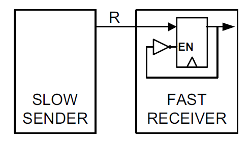
Figure 12: Slow-to-Fast "synchronizer"
图 12:慢时钟转快时钟"同步器"
EN
SLOW
SENDER
FAST
RECEIVER
使能信号 EN
慢时钟域 发送端
快时钟域 接收端
Such a simplified synchronizer typically works just fine. Except that SOCs tend to evolve and change clock frequencies. Sometimes clocks are changed during the design, when certain frequencies turn out to be too fast. In other cases, when a new product generation is launched or when the SOC is ported to a different fabrication process, slow domains may be sped up, and the assumption of who's faster may no longer hold. Hopefully the assumption has not been forgotten in the meantime, and the only adverse effect is that the chip needs to undergo a new logic and physical design, merely due to the 'optimized' synchronizer.
该简化电路在初始工况下可正常工作,但片上系统会不断迭代,时钟频率也会随之调整:设计阶段可能因速率超标下调时钟,产品迭代、工艺移植时,原本的慢时钟域可能被提速,"发送端时钟更慢"的前提不再成立。若设计人员遗忘该前置约束,这款"优化"后的同步器会导致芯片必须重新完成逻辑与物理设计。
3.11 Metastability Blocker
3.11 亚稳态阻断电路
A designer has suggested blocking metastability by the circuit of Figure 13. RESET clears the SR latch and the synchronizing flop. When the clock is high, if INPUT rises, the latch is set. When the clock goes low, the asynchronous input is blocked and only the SR latch output is connected to the flop. When the clock rises, it samples the synchronous output of the latch, rather than the asynchronous input.
有设计人员提出采用图 13 电路阻断亚稳态:复位信号 RESET 对 SR 锁存器和同步触发器清零。时钟为高电平时,输入信号跳变会置位锁存器;时钟跳转为低电平时,切断异步输入通路,仅将 SR 锁存器输出接入触发器;时钟上升沿到来时,触发器采样锁存器的同步输出,而非原始异步输入。
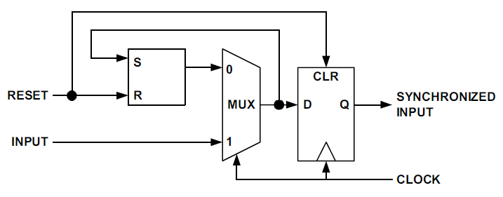
Figure 13: Metastability "blocker"
图 13:亚稳态"阻断电路"
RESET SYNCHRONIZED
INPUT
MUX
INPUT
CLOCK
复位信号 同步输出
输入信号
多路选择器 MUX
原始输入
时钟
The designer has missed two problem scenarios, though. If INPUT rises exactly when the clock goes low, the SR latch can become metastable. It will most likely settle by the next rising edge of the clock. In other words, the metastability risk has simply been transferred from the flop to the latch, and one-half clock cycle is allowed for settling. If the proper protocol is employed (e.g., INPUT stays high until acknowledged), the synchronization will function correctly.
该设计存在两处漏洞:第一,若输入信号跳变与时钟下降沿同时发生,SR 锁存器会进入亚稳态,其大概率会在下一个时钟上升沿前稳定。简言之,该电路只是将亚稳态风险从触发器转移到锁存器,仅增加半个时钟周期的稳定时长。若配合合规握手协议(例如输入信号保持高电平直至收到应答),电路可勉强正常工作。
The second scenario is more dangerous. If INPUT rises exactly when the clock rises, the SR latch will probably miss it but the flop may become metastable. While the first scenario seems to be handled properly by the circuit (in spite of the designer's ignorance), the latter case may cause damage in the circuit that follows the flop.
第二处漏洞风险更高:若输入信号跳变与时钟上升沿同时发生,SR 锁存器大概率无法捕获信号,而触发器仍会进入亚稳态。第一种场景可被电路变相缓解,但该场景会直接导致触发器后级电路工作异常。
Various "metastability blockers" or circuits that "eliminate" metastability are repeatedly reinvented and occasionally get published. Fortunately, most practitioners have learned to take them with a grain of salt.
业界不断出现各类宣称"阻断"或"消除"亚稳态的电路方案,部分还被刊发,但资深工程师均清楚这类方案并不能从本质上解决亚稳态问题。
3.12 Parallel Synchronizer
3.12 并行同步器
A careful designer assumed that more is better and, instead of using the recommended complex structure for a push synchronizer, he inserted a separate two-flop synchronizer on each data line (Figure 14). That scheme also seems to save one cycle time (no need to wait one full cycle after R2 is stable and until R E G R REG_{R} REGR latches the incoming data, as in Figure 3).
部分设计人员认为并行设计可靠性更高,放弃标准推挽式同步器架构,转而在每一条数据线上单独配置一组两级触发器同步器(图 14)。该方案看似还能节省一个时钟周期(无需像图 3 那样,等待 R2 稳定后再延时一个周期锁存数据至 R E G R REG_{R} REGR)。
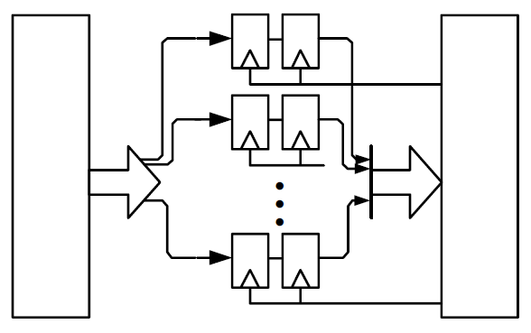
Figure 14: Parallel "synchronizer"
图 14:并行"同步器"
This scheme is a yet another prescription for a sure disaster. On clock-data conflict, each of the several data synchronizers may end up doing something different: Some may sample the new data, others may miss it and retain the old data, while yet others may enter metastability. Of the metastable ones, some may settle to '1' while others may settle to '0'. There is no way of telling which is which, as all four options are equally legitimate and possible outcomes.
该方案会引发严重故障。当出现时钟数据冲突时,各路数据同步器的状态相互独立:部分同步器采样到新数据,部分未采样到而保留旧数据,还有部分进入亚稳态;处于亚稳态的电路,最终也会随机稳定为高电平或低电平。上述各类状态均有可能出现,最终导致并行数据位错乱。
To emphasize the severity of failure, recall that a typical single synchronizer may enter metastability twice every millisecond, as computed in Section 3.1. Thus, a 32 bit parallel synchronizer faces a risk of failure every 16 microseconds!
结合 3.1 节计算结果,单个同步器平均每毫秒出现两次亚稳态。以此推算,32 位并行同步器的平均故障间隔仅为 16 微秒,故障概率极高。
Another incarnation of this problem employs three parallel synchronizers and takes a vote of their outputs. Is this any safer than the non-voting parallel synchronizer?
还有一种衍生设计:采用三路并行同步器,对输出结果做三取二表决。该方案相比无表决的并行同步器,安全性并未得到本质提升。
3.13 Shared Flop Synchronizer
3.13 共享触发器同步器
The synchronization handshake protocol is sometimes implemented with a signaling latch, set by the sender and cleared by the receiver. A somewhat misleading example based on two signaling flops has been published by a leading FPGA vendor (Figure 15). The problem is that the RECEIVE signal, which is driven by the sender's clock, is never synchronized by the receiver's (at least not in the schematics shown in the publication).
部分握手协议会采用信号锁存器实现:由发送端置位、接收端复位。某主流现场可编程门阵列厂商曾发布基于两个信号触发器的电路案例(图 15),该案例存在设计误导。电路中由发送端时钟驱动的接收信号 RECEIVE,并未经过接收端时钟同步(该问题在厂商公开原理图中明显存在)。
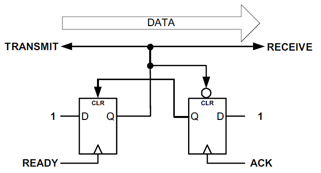
Figure 15: Shared flop "synchronizer"
图 15:共享触发器"同步器"
DATA
TRANSMIT RECEIVE
READY
ACK
数据信号
发送信号 接收信号
就绪信号
应答信号
A better scheme for a shared latch synchronizer (Figure 16) has been shown by Dike 19 and has been employed successfully in a low-voltage product (low supply voltage increases the risk of metastability). The control signals generated by the shared latch are both carefully synchronized with their respective clocks.
戴克19提出了一种合规的共享锁存器同步方案(图 16),该方案已成功应用于低压产品(低电源电压会提升亚稳态发生概率)。该设计中,共享锁存器产生的所有控制信号,均经过对应时钟域的同步处理。
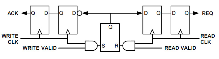
Figure 16: A correct shared latch synchronizer
图 16:合规的共享锁存器同步器
REQ
WRITE VALID
WRITE CLK
READ CLK
请求信号 REQ
写有效信号
写时钟
读时钟
3.14 Conservative Synchronizer
3.14 冗余多级同步器
The careful designer occasionally wishes to be on the safe side and, when synchronization latency is not an issue, adds "just a few more stages" to the synchronizer (Figure 17). While this is not an error, it is interesting to learn what additional level of safety is thus obtained. Considering an SOC with two clock domains where the receiver operates at 200 MHz (a reasonable frequency for the 0.18µm technology), and where data is exchanged every ten clock cycles (as a worst case), and assuming T w = 50 p s T_{w}=50 ps Tw=50ps , τ = 10 p s \tau=10 ps τ=10ps (all 'conservative' numbers), the normal two-flop MTBF is e 500 / 2 × 10 5 = 10 204 e^{500} / 2 ×10^{5}=10^{204} e500/2×105=10204 years. This is rather safe, when we recall that the age of the universe is 10 10 10^{10} 1010 years. The added cycle time provides an extra safety factor of e 500 e^{500} e500 , achieving a more comforting level of 10 420 10^{420} 10420 years. Imagine how much better MTBF could have been if you used four flops, rather than three!
部分设计人员为提升可靠性,在传输延迟无约束的前提下,额外增加同步器级数(图 17)。该设计不属于错误,下文量化分析其可靠性提升幅度。以 0.18 μm 工艺片上系统为例,接收端时钟 200 MHz,最坏工况下每 10 个时钟周期传输一次数据,取保守参数 T W = 50 ps T_{W}=50\ \text{ps} TW=50 ps、 τ = 10 ps \tau=10\ \text{ps} τ=10 ps。标准两级触发器同步器的平均无故障时间为 e 500 / 2 × 10 5 = 10 204 e^{500} / 2 ×10^{5}=10^{204} e500/2×105=10204 年,对比宇宙约 10 10 10^{10} 1010 年的年龄,该可靠性已极高。每额外增加一级触发器,安全系数提升 e 500 e^{500} e500,平均无故障时间可达 10 420 10^{420} 10420 年。以此类推,四级触发器同步器的平均无故障时间会进一步大幅提升。
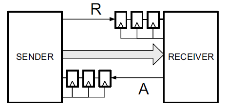
Figure 17: Conservative synchronizer
图 17:冗余多级同步器
SENDER RECEIVER
发送端 接收端
4. Conclusions
4. 结论
A few examples of synchronization design errors have been presented and analyzed. As long as there are no foolproof algorithms and tools to validate synchronizers, the rules to safe design should be closely watched. A strict design methodology and discipline should be enforced, especially prohibiting arbitrary "improvements" of synchronizers and shortcuts in their design and implementation. Optimizations that may impede future design reuse should be avoided. Knowledgeable rigorous validation should be carried out to verify that all crossings of clock domains are understood and legitimate. Global signals that span multiple domains, such as reset and clocks, should be examined carefully. Such validation should be repeated after every design change and before final design closure.
本文列举并分析了多类同步电路设计错误案例。在尚无绝对可靠的同步器验证算法与工具的现状下,设计人员必须严格遵守同步电路设计规范。执行标准化设计流程与管控要求,严禁私自对同步电路做"优化"或简化设计;杜绝因优化导致电路无法复用的设计方案。必须对所有跨时钟域路径做专业、严格的校验,确保每一条路径的同步设计均合规。复位、全局时钟等跨多时钟域信号,需重点核查。每一次电路改版、设计最终收尾前,都必须重复完成全套同步校验。
Present efforts to design synchronizer cell libraries and to develop rigorous tools for synchronization validation may help alleviate these issues and assure safe GALS SOCs.
目前业界正推进同步器标准单元库研发、专业同步验证工具开发,这些工作将逐步改善同步设计现状,保障全局异步局部同步片上系统稳定工作。
Synchronization issues may be more difficult to examine and validate with third-party IP cores, and especially "hard" cores whose internal logic design is unknown to the SOC designer. The architect should insist on at least a complete specification of their synchronizing circuits.
第三方知识产权核(尤其是内部逻辑不对外公开的硬核)的同步问题,检测与验证难度更高。芯片架构师应要求知识产权核供应商,提供完整的同步电路设计文档。
A certain type of synchronizers has not been dealt with in this paper, namely fast synchronizers for multi-sync 20 or mesochronous 4, 5 clock domains. Their design and validation are more complex and deserve another paper.
本文未覆盖多同步时钟域、准同步时钟域对应的高速同步电路4,5,20,这类电路的设计与验证更为复杂,可单独撰文探讨。
Acknowledgement
致谢
The author is grateful to the many imaginative designers whose innovations ended up in this paper. Their names are kept in confidence. The anonymous referees added some interesting examples to this catalog and helped weed out some of the bugs; the author alone should be blamed for any remaining mistakes.
笔者感谢各位工程师,本文案例均来自他们的实际设计尝试,相关人员信息予以保密。匿名审稿人为本文补充了典型案例,并协助修正文中错误;若本文仍存在疏漏,责任由笔者承担。
References
参考文献
1 J. Jex and C. Dike, "A fast resolving BiNMOS synchronizer for parallel processor interconnect," IEEE Journal of Solid-State Circuits, vol. 30, pp. 133-139, 1995.
J. 杰克斯, C. 戴克. 用于并行处理器互联的快速响应双极型 NMOS 同步器J. IEEE 固态电路期刊, 1995, 30: 133-139.
2 C. Dike and E. Burton, "Miller and Noise Effects in a Synchronizing Flip-Flop," IEEE Journal of Solid-State Circuits, vol. 34, pp. 849-855, 1999.
C. 戴克, E. 伯顿. 同步触发器中的密勒效应与噪声影响J. IEEE 固态电路期刊, 1999, 34: 849-855.
3 D. J. Kinniment, A. Bystrov, and A. Yakovlev, "Synchronization Circuit Performance," IEEE Journal of Solid-State Circuits, vol. 37, pp. 849-855, 2002.
D. J. 金尼曼特, A. 贝斯特罗夫, A. 雅科夫列夫. 同步电路性能研究J. IEEE 固态电路期刊, 2002, 37: 849-855.
4 W. J. Dally and J. W. Poulton, Digital System Engineering(Eds.): Cambridge University Press, 1998.
W. J. 戴利, J. W. 波尔顿. 数字系统工程M. 剑桥大学出版社, 1998.
5 T. H.-Y. Meng, Synchronization Design for Digital Systems(Eds.): Kluwer Academic Publishers, 1991.
孟汉源. 数字系统同步设计M. 克鲁维尔学术出版社, 1991.
6 D. J. Kinniment and J. V. Woods, "Synchronization and Arbitration Circuits in Digital Systems," Proceedings of the IEE, vol. 123, pp. 961--966, 1976.
D. J. 金尼曼特, J. V. 伍兹. 数字系统中的同步与仲裁电路J. 英国电气工程师学会会刊, 1976, 123: 961-966.
7 R. Ginosar and R. Kol, "Adaptive Synchronization," in Proc. International Conf. Computer Design (ICCD), 1998, pp. 188--189.
R. 吉诺萨尔, R. 科尔. 自适应同步技术C//国际计算机设计会议论文集, 1998: 188-189.
8 T. J. Chaney and C. E. Molnar, "Anomalous Behavior of Synchronizer and Arbiter Circuits," IEEE Transactions on Computers, vol. C-22, pp. 421--422, 1973.
T. J. 钱尼, C. E. 莫尔纳. 同步器与仲裁电路的异常工作特性J. IEEE 计算机汇刊, 1973, C-22: 421-422.
9 M. Pechoucek, "Anomalous Response Times of Input Synchronizers," IEEE Transactions on Computers, vol. 25, pp. 133--139, 1976.
M. 佩乔切克. 输入同步器的异常响应时延J. IEEE 计算机汇刊, 1976, 25: 133-139.
10 W. Fleischhammer and O. Dortok, "The anomalous behavior of flip-flops in synchronizer circuits," IEEE Transactions on Computers, vol. 28, pp. 273--276, 1979.
W. 弗莱施哈默, O. 多托克. 同步电路中触发器的异常特性J. IEEE 计算机汇刊, 1979, 28: 273-276.
11 H. J. M. Veendrick, "The Behavior of Flip-Flops Used as Synchronizers and Prediction of Their Failure Rate," IEEE Journal of Solid-State Circuits, vol. 15, pp. 169--176, 1980.
H. J. M. 温德里克. 同步触发器工作特性与失效率预测J. IEEE 固态电路期刊, 1980, 15: 169-176.
12 L. Kleeman and A. Cantoni, "Can redundancy and masking improve the performance of synchronizers," IEEE Transactions on Computers, vol. 35, pp. 643--646, 1986.
L. 克莱曼, A. 坎托尼. 冗余与屏蔽技术能否提升同步器性能J. IEEE 计算机汇刊, 1986, 35: 643-646.
13 P. Day and J. V. Woods, "Investigation into Micropipeline Latch Design Styles," IEEE Transactions on VLSI Systems, vol. 3, pp. 264-272, 1995.
P. 戴, J. V. 伍兹. 微流水线锁存器架构研究J. IEEE 超大规模集成电路系统汇刊, 1995, 3: 264-272.
14 A. Peeters and K. v. Berkel, "Single-Rail Handshake Circuits," in Asynchronous Design Methodologies: IEEE Computer Society Press, 1995, pp. 53--62.
A. 彼得斯, K. 范贝克尔. 单轨握手电路C//异步设计方法论. IEEE 计算机学会出版社, 1995: 53-62.
15 "Clock Domain Checker User Manual," Avant! Corporation v2001.3, 2001.
Avant! 公司. 时钟域检查工具用户手册v2001.3. 2001.
16 atHDL, "Multiple Clock Domain Analysis," www.athdl.com.
atHDL 公司. 多时钟域分析工具EB/OL. www.athdl.com.
17 A. V. Yakovlev, "On Limitations and Extensions of STG model for Designing Asynchronous Control Circuits," in Proc. International Conf. Computer Design (ICCD): IEEE Computer Society Press, 1992, pp. 53--62.
A. V. 雅科夫列夫. 异步控制电路设计中信号转移图模型的局限与扩展C//国际计算机设计会议论文集. IEEE 计算机学会出版社, 1992: 53-62.
18 S. Furber (Eds.): Principles of Asynchronous Circuit Design: A Systems Perspective, Kluwer Academic Publishers, 2001.
18 S. 弗伯. 异步电路设计原理:系统视角M. 克鲁维尔学术出版社, 2001.
19 C. Dike, "Sychronization Tutorial," presented at Sixth International Symposium on Advanced Research in Asynchronous Circuits and Systems (ASYNC2000), 2000.
C. 戴克. 同步技术教程R. 第六届异步电路与系统前沿研究国际研讨会, 2000.
20 R. Ginosar and R. Kol, "Adaptive Synchronization," in Proc. International Conf. Computer Design (ICCD), 1998, pp. 188--189.
R. 吉诺萨尔, R. 科尔. 自适应同步技术C//国际计算机设计会议论文集, 1998: 188-189.
十四种同步器设计误区总结
本文基于 Ran Ginosar 的论文 Fourteen Ways to Fool Your Synchronizer (ASYNC 2003)整理,原文第 3 章节共划分 14 类同步器异常设计场景,对应论文标题的十四种设计误区,同时结合工程实践补充单触发器同步器特性、风险规避方案及工业界拓展设计问题。
一、十四类同步器异常设计清单(原文 3.1 ~ 3.14)
1. 3.1 Avoiding the Synchronizer --- 直接省略同步电路
- 现象:异步时钟域之间传输信号,未添加任何同步电路。
- 诱因:设计人员低估亚稳态发生概率,或认为接收端时钟频率更高,必然可以正常采样信号。
- 危害:当信号跳变与时钟采样沿发生冲突时,触发器易进入亚稳态,造成整片逻辑工作异常。
- 典型参数 :以 f clk = 1 GHz f_{\text{clk}} = 1\ \text{GHz} fclk=1 GHz、 f data = 100 MHz f_{\text{data}} = 100\ \text{MHz} fdata=100 MHz、 T W = 20 ps T_{W} = 20\ \text{ps} TW=20 ps 为例,亚稳态进入频率可达 2 × 10 6 2 \times 10^{6} 2×10⁶ 次/秒(每 500 500 500 个时钟周期一次),风险极高。
- 检测方式:开展跨时钟域路径分析(CDC Analysis),逐一核验所有跨域路径是否完成同步处理。
2. 3.2 One Flop Synchronizer --- 单触发器同步器
- 现象:为降低传输延迟,将标准两级触发器同步器简化为单级触发器。
- 隐患:单触发器出现亚稳态、输出延迟增大时,后级组合逻辑无法在一个时钟周期内完成信号稳定。
- 合法使用条件:若触发器后端组合逻辑延迟极小,剩余信号稳定时长可满足设计指标,方可使用该结构。
- 检测规则:同步触发器输出必须直接连接同时钟域的下一级触发器,中间不得插入组合逻辑。
3. 3.3 Sneaky Path --- 隐蔽跨域路径
- 现象:电路改版、代码重构后,产生无意识且未做同步处理的跨时钟域信号通路。
- 常见场景 :
- 信号迁移至新时钟域后,未删除其在原时钟域的引用端口;
- 误用原始异步信号,而非经过同步处理的信号;
- 设计人员不明确信号所属时钟域,直接进行跨域调用。
- 处理方案:问题本质与直接省略同步电路一致,依靠跨时钟域路径排查完成整改。
4. 3.4 Greedy Path Synchronizer --- 激进路径同步器
- 现象 :使用标准两级触发器同步器,但抓取中间级信号搭建检测逻辑 D = R 1 ⋅ R 2 ‾ D = R_{1} \cdot \overline{R_{2}} D=R1⋅R2,以此压缩传输延迟。
- 隐患 :第一级触发器 R 1 R_{1} R1 出现亚稳态、响应延迟变长时,后端组合逻辑会出现时序崩溃。
- 正确做法 :延后一级采样,采用逻辑 D = R 2 ⋅ R 3 ‾ D = R_{2} \cdot \overline{R_{3}} D=R2⋅R3 搭建检测电路。
5. 3.5 Wrong Protocol --- 握手协议错误
- 现象:擅自删减握手应答链路,使用固定延时替代标准握手协议。
- 问题说明 :
- 违背握手协议单令牌安全约束,新到达的数据会覆盖尚未被处理的旧数据;
- 芯片迭代、工艺移植导致时钟频率变更后,固定延时不再适配,同步功能完全失效。
- 解决方式:统一采用标准二相位/四相位握手协议,禁止使用固定延时替代应答机制。
6. 3.6 Global Reset Synchronizer --- 全局复位同步设计错误
- 现象:在多时钟域 GALS(全局异步局部同步)系统中,全局复位信号的下降沿未做同步处理。
- 原理说明:复位上升沿(有效沿)可强制电路进入初始状态;若复位下降沿(释放沿)与时钟采样沿同时出现,接入异步复位端口的触发器会产生亚稳态。
- 正确方案 :复位信号上升沿直通传输,下降沿通过两级触发器完成同步------即 异步复位、同步释放(Async Assert, Sync Deassert)架构。
7. 3.7 Async Clear Synchronizer --- 异步清零/置位同步错误
- 现象:跨时钟域传输异步清零、置位信号,认为异步信号无需做同步处理。
- 隐患:清零/置位信号的撤销沿与接收端时钟沿冲突时,会触发触发器亚稳态。
- 解决方案 :
- 通用场景:异步清零信号通过两级触发器完成同步;
- 要求上升沿无延迟的场景:采用非对称同步电路,仅对信号下降沿(撤销沿)做同步。
8. 3.8 DFT Leakage --- 可测试性设计(DFT)路径泄露
- 现象:使用单时钟测试仪测试 GALS 芯片时,会将所有时钟短接,工程中通过伪路径(False Path)屏蔽时钟短接产生的无效路径;设计改版后,新增的错误跨域路径被伪路径清单错误屏蔽。
- 背景说明:单时钟测试仪无法区分多组时钟,测试阶段必须短接芯片所有时钟。
- 解决方式:每一次设计变更完成后,重新审核并更新伪路径列表。
9. 3.9 Pulse Synchronizer --- 简易脉冲同步器
- 现象:采用简易翻转式电路实现单周期脉冲信号的跨时钟域传输。
- 失效场景 :
- 输入脉冲连续多个时钟周期保持高电平;
- 两路脉冲信号的间隔仅为一个时钟周期。
- 整改方案:替换为标准纯控制信号同步器,并搭配二相位握手协议使用。
10. 3.10 Slow-to-Fast Synchronizer --- 慢时钟转快时钟简化同步器
- 现象:依托「发送端时钟频率低、接收端时钟频率高」的固定关系简化握手逻辑,依靠高频时钟多次采样保证信号采集。
- 缺陷说明:芯片迭代、工艺移植、时钟参数重配后,收发端时钟快慢关系可能反转,简化后的逻辑彻底失效。
- 衍生风险:该问题会导致芯片重新开展逻辑设计与物理设计。
11. 3.11 Metastability Blocker --- 伪亚稳态阻断电路
- 现象:设计人员自研电路(如 SR 锁存器 + 多路选择器架构),宣称可消除、阻断亚稳态。
- 本质问题:亚稳态仅从触发器转移至锁存器,并未被消除,部分工况下依旧会造成后级电路运行异常。
- 结论:不存在可以彻底消除亚稳态的电路结构,此类设计均不具备可靠性。
12. 3.12 Parallel Synchronizer --- 并行数据同步器
- 现象:为多比特总线的每一根数据线单独配置一组两级触发器同步器,替代标准捆绑式握手同步架构。
- 危害:发生时钟与数据冲突时,各路同步器独立动作,部分采样新数据、部分保留旧数据、部分进入亚稳态,最终造成总线数据错乱。
- 量化风险 : 32 32 32 位并行同步器的平均故障间隔(MTBF)仅为 16 μ s 16\ \mu\text{s} 16 μs。
- 补充说明:增加三模表决(TMR)结构,也无法从根源上解决该问题。
13. 3.13 Shared Flop Synchronizer --- 错误版共享触发器/锁存器同步器
- 现象:使用收发端共用的信号锁存器、触发器搭建握手电路,但跨时钟域控制信号未做同步处理,该问题曾出现在 FPGA 厂商公开范例中。
- 正确方案(Dyke 方案):共享锁存器输出的所有控制信号,分别按照所属时钟域完成同步,该方案已在低压工艺产品中落地应用。
14. 3.14 Conservative Synchronizer --- 过度冗余多级同步器
- 现象:在无传输延迟约束的场景下,为追求安全性,在标准两级同步器基础上持续增加触发器级数。
- 定性说明:该结构不属于功能错误,属于过度设计。
- 量化参考 :标准两级同步器的 MTBF(平均故障间隔)在典型工况下可达 10 14 10^{14} 1014 年量级(远超宇宙年龄 10 10 10^{10} 1010 年量级);继续增加触发器级数会使 MTBF 呈指数增长,但会无谓增大传输延迟。
二、十四类同步器异常整体分类
按照问题成因与应用场景,将十四类设计划分为五大类别:
-
基础同步缺失/简化错误(第 1 ~ 4 类)
包含省略同步电路、单触发器同步器、隐蔽跨域路径、激进路径同步器,均为压缩延迟、简化电路引发的基础设计问题。
-
协议与全局信号错误(第 5 ~ 8 类)
包含握手协议错误、全局复位同步错误、异步清零同步错误、DFT 路径泄露,属于系统级、全局信号的同步设计问题。
-
特定信号专用同步器错误(第 9 ~ 10 类)
包含简易脉冲同步器、慢转快时钟简化同步器,电路设计依赖固定时钟关系,通用性较差。
-
原理认知类错误(第 11 ~ 12 类)
包含伪亚稳态阻断电路、并行数据同步器,由设计人员对亚稳态、总线同步原理理解不足导致。
-
架构选型与冗余设计(第 13 ~ 14 类)
包含错误版共享触发器同步器、过度冗余多级同步器,属于电路架构选型与工程取舍类问题。
三、单触发器同步器特性与风险规避
3.1 单触发器同步器优缺点
优点
- 传输延迟更低:相比标准两级触发器同步器,减少一级寄存器的时延,适用于对延迟要求严苛的接口。
- 面积与功耗更小:减少触发器、时钟负载与布线资源,降低芯片面积、动态功耗及时钟树开销。
- 实现简单:电路结构与 HDL 代码更简洁,上手难度低。
缺点
-
亚稳态耐受能力弱:两级同步器可利用一个时钟周期让第一级触发器脱离亚稳态,单触发器无缓冲环节,时钟数据冲突后输出会长时间不稳定。
-
易引发时序违规:若同步触发器后端接入组合逻辑,亚稳态带来的超长延迟,会导致下一级触发器不满足建立时间要求,触发功能错误。
-
平均故障间隔劣化 :组合逻辑延迟 d d d 会挤占信号稳定窗口 T res T_{\text{res}} Tres,有效稳定时长变为 T res − d T_{\text{res}} - d Tres−d。同步器平均故障间隔公式:
MTBF = e T res / τ T W ⋅ f clk ⋅ f data \text{MTBF} = \frac{e^{\,T_{\text{res}} / \tau}}{T_{W} \cdot f_{\text{clk}} \cdot f_{\text{data}}} MTBF=TW⋅fclk⋅fdataeTres/τ
其中:
- T res T_{\text{res}} Tres:可用亚稳态恢复时间(resolution time);
- τ \tau τ:触发器亚稳态时间常数(工艺相关,现代 CMOS 工艺约 20 ∼ 50 ps 20 \sim 50\ \text{ps} 20∼50 ps);
- T W T_{W} TW:亚稳态窗口(aperture time,约等于建立时间 + 保持时间);
- f clk f_{\text{clk}} fclk:接收端时钟频率;
- f data f_{\text{data}} fdata:数据跳变频率。
有效稳定时长缩短后,MTBF 呈指数下降,故障概率上升。
-
适用范围有限:仅可在严格时序约束下使用,芯片迭代、工艺切换、时钟调频后易出现故障。
3.2 单触发器同步器风险规避方案
1. 受限场景下合规使用(必须采用单触发器时)
- 后端布线规则:同步触发器输出直接连接同时钟域的下一级触发器,中间禁止插入任何组合逻辑。
- 时序评估 :核算组合逻辑延迟 d d d,保证 T res − d T_{\text{res}} - d Tres−d 满足项目规定的 MTBF 指标,不达标则禁止使用。
- 场景限制:仅用于低速、低吞吐、非关键控制信号,禁止应用在高速总线、全局使能、复位等关键信号通路。
- 专项时序检查:在静态时序分析(STA)中对该路径单独添加约束,重点核验建立时间、保持时间与亚稳态恢复窗口。
2. 最优方案:替换为标准两级触发器同步器(推荐)
- 通用异步时钟域跨信号传输,统一采用两级触发器同步器,利用完整时钟周期作为亚稳态恢复时间,保证 MTBF 覆盖产品全生命周期。
- 搭配标准二相位/四相位握手协议,兼顾数据完整性与同步可靠性。
3. 折中延时优化方案
若存在严苛的延迟压力,保留两级同步器架构,通过优化时钟树、选用高速触发器、精简走线等方式降低延迟,不降级为单触发器结构。
四、工业界拓展高频同步设计误区
以下为论文未提及、工程实践中常见的同步设计问题:
- 同步器跨电压/电源域无处理:不同电压域的异步信号直接接入同步器,电平不匹配导致采样错误。
- 同步器增加时钟门控/使能信号:标准同步器使用门控时钟、片选使能,破坏亚稳态恢复时序,标准同步器必须使用自由运行时钟(free-running clock)。
- 滥用多周期路径约束:将跨时钟域路径设置为多周期路径,以此替代同步电路,本质仍为裸信号跨域。
- 同步器穿插大量组合逻辑:触发器前后插入多级组合逻辑,压缩亚稳态恢复时间。
- 差分接口省略同步:认为差分信号抗干扰能力强,异步时钟域下不做同步处理,依旧会产生亚稳态。
- 复位逻辑混用同步/异步复位:同步器内部触发器混用两种复位方式,复位沿与时钟沿冲突引发故障。
五、通用同步设计准则
- 异步时钟域之间的信号传输必须做同步处理,禁止裸信号直接跨域连接。
- 通用场景优先采用两级触发器同步器 + 标准握手协议,不随意简化电路、修改协议。
- 并行总线采用数据捆绑 + 控制信号握手架构,禁止对每一根数据线单独同步。
- 全局复位、异步清零等跨域异步控制信号,需针对信号边沿做专项同步设计。
- 禁止依托固定时钟频率、快慢关系做定制化简化设计,芯片迭代会打破预设条件。
- 不存在可彻底消除亚稳态的电路结构,仅能通过合理设计同步器提升平均故障间隔(MTBF)。
reference
- Fourteen ways to fool your synchronizer - Asynchronous Circuits and Systems, 2003. ..
https://dl.acm.org/doi/10.5555/785169.785383