高级边界扫描 --8-- 使用TAP控制器状态图
文章目录
- [高级边界扫描 --8-- 使用TAP控制器状态图](#高级边界扫描 --8-- 使用TAP控制器状态图)
-
-
- 使用TAP控制器状态图
- 链列表表单
- 使用MSPD进行测试开发
- 将源代码导入到电路板测试中
- [示例 VCL 源代码文件](#示例 VCL 源代码文件)
-
使用TAP控制器状态图
MSPD中的TAP控制器状态图与SPD的工作方式相同。用于为设备链中的设备创建自定义测试。您可以为整个链编写测试,也可以为链中的单个设备编写测试。
MSPD的一个关键点是,当您为整个链开发测试时,只需要一个状态图。因为链中每个设备总是处于相同的状态,因此从一个状态移动到另一个状态所需的矢量不必为链中的每个设备生成。
设备将全部处于相同的TAP状态,但每个设备可能有不同的指令和不同的数据。例如,一个可能在EXTEST状态,而其他的在HIGHZ或BYPASS状态。
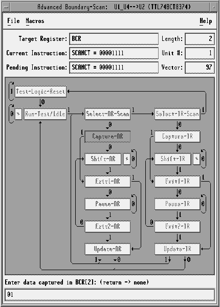
单击Shift-DR迭代器按钮会在状态区域显示链中某个设备的信息。MSPD标题栏指示您需为哪个设备输入数据。
在提示捕获数据时,软件会自动跳过BYPASS状态的设备(因为它知道BYPASS捕获什么),并停在第一个分配了除BYPASS以外指令的设备上。在提示要移入目标寄存器的数据时,软件按照顺序通过链,从tdi设备到tdo设备。
用户输入区域显示一个提示,要求您输入适当的数据。接下来的交互过程类似于旧界面的操作(例如,为选定设备和指令捕获或移入的数据)。提示基于目标寄存器和当前指令。
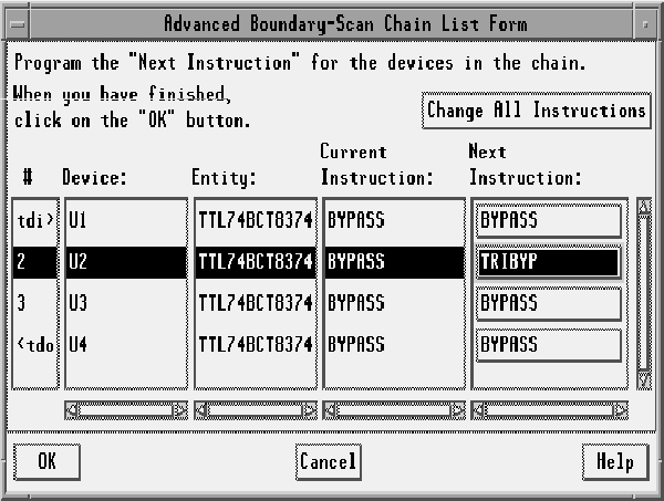
链列表表单仅出现在MSPD界面中。它允许您为链中的设备指定下一个指令。
链列表表单
点击TAP控制器状态图中IR列的迭代按钮会打开链列表表单(图7-3)。该表单包含链中所有设备的表格。表格显示以下内容:
-
第一列标识设备在链中的位置。tdi>标识告诉您该设备是链中的第一个,<tdo标识标识链中的最后一个设备。
-
第二和第三列通过提供它们的参考设计符(例如U1,U2)及其相关的实体名称(例如TTL74bct8374)来标识设备,这些信息在BSDL文件中找到。
-
第四列显示每个设备的当前指令,而最后一列显示下一个要执行的指令。下一个指令是您可以在此表单中编程的内容。
-
仅限TAP的设备将在表中显示为灰色;此类设备既不能选择也不能更改。
链列表表单
链列表表单允许您通过两种方式为设备指定下一个指令:
要更改单个设备的下一个指令
- 点击"下一个指令"列中的空格。
这会显示一个新窗口,其中列出了该设备可能的指令(从BSDL文件中提取)。
- 从列表中选择指令,然后点击"选择"按钮返回链列表表单。
如果列表中显示了PRIVATE指令,您必须谨慎操作以确保每个测试按制造商的意图进行处理。如果您不知道PRIVATE指令的功能,则不应将其包含在您的测试中。
要更改链中每个设备的指令
- 点击表单顶部附近的"更改所有指令",然后从下拉列表中选择指令(BYPASS,SAMPLE或EXTEST)。
当您在链列表表单中点击确定按钮时,新指令集的矢量被写入。
每当您调用链列表表单时,即使您决定取消表单,也会为链中的每个设备写入矢量。这是因为您从TAP状态图中调用该表单;必须发生一系列状态更改才能使图返回到一个新的起点。
使用MSPD进行测试开发
MSPD帮助您为边界扫描设备链开发自定义测试。在MSPD工作区中:
-
状态区域帮助您了解在链中设备的测试生成过程中的位置,
-
TAP控制器状态图允许您对设备进行编程以满足特定的测试需求,
-
用户输入区域提示您输入继续测试生成过程所需的数据。
点击Shift-DR迭代器按钮会显示链中某个设备的状态信息。如图7-4所示,MSPD标题栏指示您需为哪个设备输入数据。
在提示捕获数据时,软件会自动跳过BYPASS状态的设备(因为它知道BYPASS捕获什么),并停在第一个分配了除BYPASS以外指令的设备上。在提示要移入目标寄存器的数据时,软件按照顺序通过链,从tdi设备到tdo设备。所需数据将依赖于目标寄存器和当前指令。
选定一个设备进行测试开发
一个示例链编程会话
在本次会话中,您将为示例边界扫描设备链开发一个INTEST功能。此测试的典型用途是检测电路设计中是否将74bct8374替换为74bct8373。由于这两个设备的边界扫描实现和引脚排列是相同的,您只能通过运行系统逻辑来区分它们。您只需要为设备u1添加此功能。
这些设备的系统逻辑包含八个触发器(8374)或八个D锁存器(8373)。您可以通过操作存储器元素来区分这两者,这样软件可以区分边沿触发设备和D锁存器。边界扫描INTEST提供了这种功能。
图7-5
比较目标设备的存储逻辑
表7-1
输出C和Z提供所需的区分器
| A | B | C | 相对模式 | X | Y | Z |
|---|---|---|---|---|---|---|
| 0 | 0 | X | #1 | 0 | 0 | X |
| 0 | 1 | 0 | #2 | 0 | 1 | 0 |
| 1 | 1 | 0 | #3 | 1 | 1 | 1 |
您可以将图7-5和表7-1中显示的输入与表7-2中位15-8的任意输入相关联;输出也可以与表7-2中的任意输出相关联。
- 开发测试策略。本次会话中,您将:
-
将u2、u3和u4置于BYPASS中
-
将u1置于SAMPLE/PRELOAD中,以便预装一个模式,称为背景模式,该模式禁用u1的驱动器。
-
将u1更改为INTEST以应用测试8374所有八个触发器所需的模式。表7-2显示了您将应用的模式。背景模式中的位16为1,这禁用了设备驱动器。其他位为X(无关)。请注意,在每个后续模式中,第16位保持为1。
请参阅示例BSDL描述以了解74bct8374单元功能。
表7-2
按系统逻辑I/O书写的模式
| 单元编号 | 17 | 16 | 15 | 14 | 13 | 12 | 11 | 10 | 9 | 8 | 7 | 6 | 5 | 4 | 3 | 2 | 1 | 0 |
|---|---|---|---|---|---|---|---|---|---|---|---|---|---|---|---|---|---|---|
| 背景模式 | X | 1 | X | X | X | X | X | X | X | X | X | X | X | X | X | X | X | X |
| 模式 #1 | 0 | 1 | 0 | 0 | 0 | 0 | 0 | 0 | 0 | 0 | X | X | X | X | X | X | X | X |
| 模式 #2 | 1 | 1 | 0 | 0 | 0 | 0 | 0 | 0 | 0 | 0 | L | L | L | L | L | L | L | L |
| 模式 #3 | 1 | 1 | 1 | 1 | 1 | 1 | 1 | 1 | 1 | 1 | L | L | L | L | L | L | L | L |
位17-8是输入位,而位7-0是输出位。表7-2向您展示了设备内部逻辑的输入和输出。表7-3向您展示了设备边界寄存器的输入和输出。
- 由于设备内部逻辑的输出不能与呈现给内部逻辑的输入同时捕获,因此表7-2中显示的模式必须被分割。然后可以将这些模式引入到边界寄存器中,这样在UPDATE-DR应用的模式(例如,模式2u)产生用于内部逻辑的正确刺激模式,然后在CAPTURE-DR时捕获(例如,模式3c)。
要从边界寄存器中获得最后一个捕获的模式,您必须添加一个刷新模式(4c和4u);请注意,背景模式用于此功能。
表7-3
示例链编程会话的模式(按边界寄存器书写)
| 单元编号 | 17 | 16 | 15 | 14 | 13 | 12 | 11 | 10 | 9 | 8 | 7 | 6 | 5 | 4 | 3 | 2 | 1 | 0 |
|---|---|---|---|---|---|---|---|---|---|---|---|---|---|---|---|---|---|---|
| 背景模式 | X | 1 | X | X | X | X | X | X | X | X | X | X | X | X | X | X | X | X |
| 模式 1c | X | X | X | X | X | X | X | X | X | X | X | X | X | X | X | X | X | X |
| 模式 1u | 0 | 1 | 0 | 0 | 0 | 0 | 0 | 0 | 0 | 0 | X | X | X | X | X | X | X | X |
| 模式 2c | X | X | X | X | X | X | X | X | X | X | X | X | X | X | X | X | X | X |
| 模式 2u | 1 | 1 | 0 | 0 | 0 | 0 | 0 | 0 | 0 | 0 | X | X | X | X | X | X | X | X |
| 模式 3c | X | X | X | X | X | X | X | X | X | X | L | L | L | L | L | L | L | L |
| 模式 3u | 1 | 1 | 1 | 1 | 1 | 1 | 1 | 1 | 1 | 1 | X | X | X | X | X | X | X | X |
| 刷新模式4c | X | X | X | X | X | X | X | X | X | X | L | L | L | L | L | L | L | L |
| 刷新模式4u | X | 1 | X | X | X | X | X | X | X | X | X | X | X | X | X | X | X | X |
- 创建一个自定义ITL源文件。
在您可以使用MSPD生成自定义测试之前,您必须创建一个自定义ITL源文件(编写ITL源文件描述了过程)。您可以在本次会话中使用示例文件示例7-2。
示例7-2
ITL源文件
plaintext
custom "u1_u4"

chain "u1_u4"

  tdi "TDI"

  tdo "TDO"

  tms "TMS"

  tck "TCK"

  devices

    "u1", "../demo_original/custom/74bct8374", "DW_PACKAGE", no

    "u2", "../demo_original/custom/74bct8374", "DW_PACKAGE", no

    "u3", "../demo_original/custom/74bct8374", "DW_PACKAGE", no

    "u4", "../demo_original/custom/74bct8374", "DW_PACKAGE", no

  end devices

end chain

nodes

end nodes

end interconnect- 自定义ITL源文件创建完成后,启动MSPD。指定自定义ITL文件作为输入,并指定一个VCL输出文件名,例如INTEST_8374。
示例7-3中的示例mspd.log文件显示了几条注释。您可以使用添加注释宏在需要的地方添加注释。
- 点击Shift-IR迭代器按钮。
在链列表表单中,所有设备指令显示为BYPASS。
a. 点击u1的下一条指令列。
b. 在指令选择表单中,选择SAMPLE指令,然后点击选择。
c. 在链列表表单中点击确定。
- 点击Shift-DR迭代器按钮。
您将看到以下提示。输入表7-3中提供的模式。
输入设备U1的BOUNDARY18寄存器的数据。
(输入背景模式。)
输入设备U2的BYPASS1寄存器的数据。
(输入X。)
输入设备U3的BYPASS1寄存器的数据。
(输入X。)
输入设备U4的BYPASS1寄存器的数据。
(输入X。)
- 点击Shift-IR迭代器按钮。
在链列表表单中,指令显示为u1的SAMPLE,其他设备的BYPASS。
a. 点击u1的下一条指令列。
b. 在指令选择表单中,选择INTEST指令,然后点击选择。
c. 在链列表表单中点击确定。
- 点击Shift-DR迭代器按钮。
输入以下消息中适当的模式。
在BOUNDARY18中捕获的数据:(按回车键 -> 无)
(输入模式1c。)
输入设备U1的BOUNDARY18寄存器中的数据。
(输入模式1u。)
输入设备U2的BYPASS1寄存器中的数据。
(输入X。)
输入设备U3的BYPASS1寄存器中的数据。
(输入X。)
输入设备U4的BYPASS1寄存器中的数据。
(输入X。)
- 点击Shift-DR迭代器按钮。
输入以下消息中适当的模式。
在BOUNDARY18中捕获的数据:(按回车键 -> 无)
(输入模式2c。)
输入设备U1的BOUNDARY18寄存器中的数据。
(输入模式2u。)
输入设备U2的BYPASS1寄存器中的数据。
(输入X。)
输入设备U3的BYPASS1寄存器中的数据。
(输入X。)
输入设备U4的BYPASS1寄存器中的数据。
(输入X。)
- 点击Shift-DR迭代器按钮。
输入以下消息中适当的模式。
在BOUNDARY18中捕获的数据:(按回车键 -> 无)
(输入模式3c。)
输入设备U1的BOUNDARY18寄存器中的数据。
(输入模式3u。)
输入设备U2的BYPASS1寄存器中的数据。
(输入X。)
输入设备U3的BYPASS1寄存器中的数据。
(输入X。)
输入设备U4的BYPASS1寄存器中的数据。
(输入X。)
- 点击Shift-DR迭代器按钮。
输入以下消息中适当的模式。
在BOUNDARY18中捕获的数据:(按回车键 -> 无)
(输入模式4c。)
输入设备U1的BOUNDARY18寄存器中的数据。
(输入模式4u。)
输入设备U2的BYPASS1寄存器中的数据。
(输入X。)
输入设备U3的BYPASS1寄存器中的数据。
(输入X。)
输入设备U4的BYPASS1寄存器中的数据。
(输入X。)
- 从文件菜单中选择保存。退出MSPD。
检查mspd.log文件和VCL输出文件。示例在示例7-3和示例7-4中提供。
使用mspd.log文件进行测试生成
当您运行MSPD时,测试会话期间执行的每个操作都会记录在名为mspd.log的文件中。每次运行MSPD时,它都会覆盖mspd.log文件。您可以使用mspd.log文件开发您的边界扫描测试。
mspd.log文件的应用原则上与单设备测试时相同。该过程在使用spd.log文件进行测试生成中有所描述。
示例7-3展示了示例链编程会话的mspd.log文件。添加了多个注释以便您可以轻松区分每个步骤。当您进行实际的编程会话时,注释可以对您的测试开发有所帮助。
示例7-3
示例mspd.log文件
add_comment

********** Beginning Sample Test Session **********

********** Clicking on Shift‑IR iterator button **********

********** Modifying U1 to SAMPLE **********

scan_instr

Instr/Dev? U1

Dev/Instr: U1 SAMPLE

Dev/Instr: U2 BYPASS

Dev/Instr: U3 BYPASS

Dev/Instr: U4 BYPASS

InstrDone.

add_comment

********** Clicking on Shift‑DR iterator button **********

********** Entering background pattern for U1 **********

scan_data

x1xxxxxxxxxxxxxxxx

x

x

x

add_comment

********** Clicking on Shift‑IR iterator button **********

********** Modifying U1 to INTEST **********

scan_instr

Instr/Dev? U1

Dev/Instr: U1 INTEST

Dev/Instr: U2 BYPASS

Dev/Instr: U3 BYPASS

Dev/Instr: U4 BYPASS

InstrDone.

add_comment

********** Clicking on Shift‑DR iterator button **********

********** Entering patterns 1c and 1u **********

scan_data

xxxxxxxxxxxxxxxxxx

0100000000xxxxxxxx

x

x

x

add_comment

********** Clicking on Shift‑DR iterator button **********

********** Entering patterns 2c and 2u **********

********** Will repeat this process two more times **********

********** for patterns 3c/3u and 4c/4u **********

scan_data

xxxxxxxxxxxxxxxxxx

1100000000xxxxxxxx

x

x

x

scan_data

xxxxxxxxxxllllllll

1111111111xxxxxxxx

x

x

x

scan_data

xxxxxxxxxxllllllll

x1xxxxxxxxxxxxxxxxxx

x

x

x

add_comment

********** Sample Test Session Completed **********

********** Selecting RESET item from MACROS menu **********

reset_tap

save
将源代码导入到电路板测试中
当您在I/O规格表中指定VCL输出文件的路径时,应将路径指向电路板测试目录。这样,VCL源代码文件将自动被包含在适当的目录中。
由于MSPD生成的是数字源代码,该文件被赋予了src(源)数字类型并进行校验和,因此它是完整的并准备好进行编译。样例源代码中的第一行(以!!!标识)包含一个代码,该代码告知测试仪该文件是数字源代码。在i3070 ICT系统的所有VCL输出文件中均包含这一行。
示例 VCL 源代码文件
示例 7-4 显示了在示例链编程会话期间生成的测试程序。
源代码包括以下注释:
- 告知您一系列矢量将执行的特定操作
- 告知您设备的当前 TAP 状态
- 指出设备特定单元的数据正从 TDO 移出
- 指出特定矢量影响了哪个单元位置以及对应的链位置
VCL 文件中的注释可以帮助您在调试期间找到特定的矢量。如果您想快速从源代码的一部分移动到另一部分,可以使用 BT-Basic 编辑器搜索您想要检查的附近矢量。软件允许您以 25 个矢量为增量进行搜索。例如,如果您想找到矢量 10038,因为它失败了,您可以打开一个 BT-Basic 窗口并输入:
findn "! vector 10025"因为矢量 10025 是与目标矢量最近出现的注释。
示例 7-4
边界扫描链的示例 VCL 源代码
sh
!!!!    6    0    1  703446703  V043a
! ********** Beginning Sample Test Session **********
! ********** Clicking on Shift‑IR iterator button **********
! ********** Modifying U1 to SAMPLE **********
! Boundary‑Scan Software [920406]
! IEEE Std 1149.1‑1990, BSDL (Version 0.0)
! ITL Test Source File:      /users/scan_brd/digital/u1_u4_cs
! Test Name:                 U1_U4
! VCL created for chain:     U1_U4
! Date: Thu Apr 16 11:53:23 1992
 !! Writing code for 3070 family.
! Chain Composition (TDI to TDO)
! Device     Entity       Package      BSDL File
! ‑‑‑‑‑‑‑‑‑  ‑‑‑‑‑‑‑‑‑‑‑  ‑‑‑‑‑‑‑‑‑‑‑  ‑‑‑‑‑‑‑‑‑‑‑‑‑‑‑‑‑
! U1         TTL74BCT8374 DW_PACKAGE   /users/scan_brd/digital/74bct8374
! U2         TTL74BCT8374 DW_PACKAGE   /users/scan_brd/digital/74bct8374
! U3         TTL74BCT8374 DW_PACKAGE   /users/scan_brd/digital/74bct8374
! U4         TTL74BCT8374 DW_PACKAGE   /users/scan_brd/digital/74bct8374
sequential ! Test U1_U4
vector cycle  200n
receive delay 100n
assign TCK  to nodes "TCK"
assign TDI  to nodes "TDI"
assign TDO  to nodes "TDO"
assign TMS  to nodes "TMS"
family TTL !! Warning, Defaulted family
inputs  TCK
inputs  TMS
inputs  TDI
outputs TDO
pcf order default Scan is   TCK,  TMS,  TDI,  TDO
!Column‑to‑Node Map, Nodes 1 to 4
!TTTT!
!CMDD!
!KSIO!
!    !
!
!
unit "Scan_Test" ! Vector 1
pcf
use pcf order Scan
"01ZX"
"11ZX"
"01ZX"
"11ZX"
"01ZX"
"11ZX"
"01ZX"
"11ZX"
"01ZX"
"11ZX"!Test‑Logic‑Reset
"00ZX"
"10ZX"!Run‑Test/Idle
"01ZX"
"11ZX"!Select‑DR‑Scan
"01ZX"
"11ZX"!Select‑IR‑Scan
"00ZX"
"10ZX"!Capture‑IR
"00ZX"
"10ZX"!Shift‑IR
end pcf
message "IEEE Std 1149.1‑1990 Integrity Failure"
message "  Device U4 has failed,"
message "  suspect device or these pins:"
message "  (tck)  13"
message "  (tms)  12"
message "  (tdi)  14"
message "  (tdo)  11"
pcf
use pcf order Scan
"000H"!0+0
"100X"
"001L"!1
"101X"
! Loading device U4 with instruction BYPASS(11111111).
"001L"!0+2 Vector 25
"101X"
"001L"!1
"101X"
"001L"!2
"101X"
"001L"!3
"101X"
"001L"!4
"101X"
"001H"!5
"101X"
end pcf
message "IEEE Std 1149.1‑1990 Integrity Failure"
message "  Device U3 has failed,"
message "  suspect device or these pins:"
message "  (tck)  13"
message "  (tms)  12"
message "  (tdi)  14"
message "  (tdo)  11"
pcf
use pcf order Scan
"001H"!6
"101X"
"001L"!7
"101X"
! Loading device U3 with instruction BYPASS(11111111).
"001L"!0+10
"101X"
"001L"!1
"101X"
"001L"!2
"101X"
"001L"!3
"101X"
"001L"!4
"101X"! Vector 50
"001H"!5
"101X"
end pcf
message "IEEE Std 1149.1‑1990 Integrity Failure"
message "  Device U2 has failed,"
message "  suspect device or these pins:"
message "  (tck)  13"
message "  (tms)  12"
message "  (tdi)  14"
message "  (tdo)  11"
pcf
use pcf order Scan
"001H"!6
"101X"
"001L"!7
"101X"
! Loading device U2 with instruction BYPASS(11111111).
"001L"!0+18
"101X"
"001L"!1
"101X"
"001L"!2
"101X"
"001L"!3
"101X"
"001L"!4
"101X"
"001H"!5
"101X"
end pcf
message "IEEE Std 1149.1‑1990 Integrity Failure"
message "  Device U1 has failed,"
message "  suspect device or these pins:"
message "  (tck)  13"
message "  (tms)  12"
message "  (tdi)  14"
message "  (tdo)  11"
pcf
use pcf order Scan
"001H"!6
"101X"
"001L"!7
"101X"
! Loading device U1 with instruction SAMPLE(00000010).
"000L"!0+26
"100X"
"001L"!1 Vector 75
"101X"
"000L"!2
"100X"
"000L"!3
"100X"
"000L"!4
"100X"
"000H"!5
"100X"
"000L"!6
"100X"
"010H"!7
"110X"!Exit1‑IR
"01ZX"
"11ZX"!Update‑IR
end pcf
message ""
pcf
! ********** Clicking on Shift‑DR iterator button **********
! ********** Entering background pattern for U1 **********
use pcf order Scan
"01ZX"
"11ZX"!Select‑DR‑Scan
"00ZX"
"10ZX"!Capture‑DR
"00ZX"
"10ZX"!Shift‑DR
! Loading device U4 register BYPASS[1] (for BYPASS).
end pcf
message "IEEE Std 1149.1‑1990 Integrity Failure"
message "  Device U4 has failed,"
message "  suspect device or these pins:"
message "  (tck)  13"
message "  (tms)  12"
message "  (tdi)  14"
message "  (tdo)  11"
pcf
use pcf order Scan
"00ZL"!0+0
"10ZX"
! Loading device U3 register BYPASS[1] (for BYPASS).
end pcf
message "IEEE Std 1149.1‑1990 Integrity Failure"
message "  Device U3 has failed,"
message "  suspect device or these pins:"
message "  (tck)  13"
message "  (tms)  12"
message "  (tdi)  14"
message "  (tdo)  11"
pcf
use pcf order Scan
"00ZL"!1+0
"10ZX"! Vector 100
! Loading device U2 register BYPASS[1] (for BYPASS).
end pcf
message "IEEE Std 1149.1‑1990 Integrity Failure"
message "  Device U2 has failed,"
message "  suspect device or these pins:"
message "  (tck)  13"
message "  (tms)  12"
message "  (tdi)  14"
message "  (tdo)  11"
pcf
use pcf order Scan
"00ZL"!2+0
"10ZX"
! Loading device U1 register BOUNDARY[18] (for SAMPLE).
end pcf
message "IEEE Std 1149.1‑1990 Integrity Failure"
message "  Device U1 has failed,"
message "  suspect device or these pins:"
message "  (tck)  13"
message "  (tms)  12"
message "  (tdi)  14"
message "  (tdo)  11"
pcf
use pcf order Scan
"00ZX"!3+0
"10ZX"
"00ZX"!1
"10ZX"
"00ZX"!2
"10ZX"
"00ZX"!3
"10ZX"
"00ZX"!4
"10ZX"
"00ZX"!5
"10ZX"
"00ZX"!6
"10ZX"
"00ZX"!7
"10ZX"
"00ZX"!8
"10ZX"
"00ZX"!9
"10ZX"
"00ZX"!10
"10ZX"
"00ZX"!11 Vector 125
"10ZX"
"00ZX"!12
"10ZX"
"00ZX"!13
"10ZX"
"00ZX"!14
"10ZX"
"00ZX"!15
"10ZX"
"001X"!16
"101X"
"01ZX"!17
"11ZX"!Exit1‑DR
"01ZX"
"11ZX"!Update‑DR
end pcf
message ""
pcf
! ********** Clicking on Shift‑IR iterator button **********
! ********** Modifying U1 to INTEST **********
use pcf order Scan
"01ZX"
"11ZX"!Select‑DR‑Scan
"01ZX"
"11ZX"!Select‑IR‑Scan
"00ZX"
"10ZX"!Capture‑IR
"00ZX"
"10ZX"!Shift‑IR
! Loading device U4 with instruction BYPASS(11111111).
"001H"!0+0
"101X"! Vector 150
"001L"!1
"101X"
"001L"!2
"101X"
"001L"!3
"101X"
"001L"!4
"101X"
"001L"!5
"101X"
"001L"!6
"101X"
"001H"!7
"101X"
! Loading device U3 with instruction BYPASS(11111111).
"001H"!0+8
"101X"
"001L"!1
"101X"
"001L"!2
"101X"
"001L"!3
"101X"
"001L"!4
"101X"
"001L"!5 Vector 175
"101X"
"001L"!6
"101X"
"001H"!7
"101X"
! Loading device U2 with instruction BYPASS(11111111).
"001H"!0+16
"101X"
"001L"!1
"101X"
"001L"!2
"101X"
"001L"!3
"101X"
"001L"!4
"101X"
"001L"!5
"101X"
"001L"!6
"101X"
"001H"!7
"101X"
! Loading device U1 with instruction INTEST(00000011).
"001H"!0+24
"101X"
"001L"!1
"101X"! Vector 200
"000L"!2
"100X"
"000L"!3
"100X"
"000L"!4
"100X"
"000L"!5
"100X"
"000L"!6
"100X"
"010H"!7
"110X"!Exit1‑IR
"01ZX"
"11ZX"!Update‑IR
! ********** Clicking on Shift‑DR iterator button **********
! ********** Entering patterns 1c and 1u **********
"01ZX"
"11ZX"!Select‑DR‑Scan
"00ZX"
"10ZX"!Capture‑DR
"00ZX"
"10ZX"!Shift‑DR
! Loading device U4 register BYPASS[1] (for BYPASS).
end pcf
message "IEEE Std 1149.1‑1990 Integrity Failure"
message "  Device U4 has failed,"
message "  suspect device or these pins:"
message "  (tck)  13"
message "  (tms)  12"
message "  (tdi)  14"
message "  (tdo)  11"
pcf
use pcf order Scan
"00ZL"!0+0
"10ZX"
! Loading device U3 register BYPASS[1] (for BYPASS).
end pcf
message "IEEE Std 1149.1‑1990 Integrity Failure"
message "  Device U3 has failed,"
message "  suspect device or these pins:"
message "  (tck)  13"
message "  (tms)  12"
message "  (tdi)  14"
message "  (tdo)  11"
pcf
use pcf order Scan
"00ZL"!1+0
"10ZX"
! Loading device U2 register BYPASS[1] (for BYPASS).
end pcf
message "IEEE Std 1149.1‑1990 Integrity Failure"
message "  Device U2 has failed,"
message "  suspect device or these pins:"
message "  (tck)  13"
message "  (tms)  12"
message "  (tdi)  14"
message "  (tdo)  11"
pcf
use pcf order Scan
"00ZL"!2+0 Vector 225
"10ZX"
! Loading device U1 register BOUNDARY[18] (for INTEST).
end pcf
message "IEEE Std 1149.1‑1990 Integrity Failure"
message "  Device U1 has failed,"
message "  suspect device or these pins:"
message "  (tck)  13"
message "  (tms)  12"
message "  (tdi)  14"
message "  (tdo)  11"
pcf
use pcf order Scan
"00ZX"!3+0
"10ZX"
"00ZX"!1
"10ZX"
"00ZX"!2
"10ZX"
"00ZX"!3
"10ZX"
"00ZX"!4
"10ZX"
"00ZX"!5
"10ZX"
"00ZX"!6
"10ZX"
"00ZX"!7
"10ZX"
"000X"!8
"100X"
"000X"!9
"100X"
"000X"!10
"100X"
"000X"!11
"100X"! Vector 250
"000X"!12
"100X"
"000X"!13
"100X"
"000X"!14
"100X"
"000X"!15
"100X"
"001X"!16
"101X"
"010X"!17
"110X"!Exit1‑DR
"01ZX"
"11ZX"!Update‑DR
end pcf
message ""
pcf
! ********** Clicking on Shift‑DR iterator button **********
! ********** Entering patterns 2c and 2u **********
! ********** Will repeat this process two more times **********
! ********** for patterns 3c/3u and 4c/4u **********
use pcf order Scan
"01ZX"
"11ZX"!Select‑DR‑Scan
"00ZX"
"10ZX"!Capture‑DR
"00ZX"
"10ZX"!Shift‑DR
! Loading device U4 register BYPASS[1] (for BYPASS).
end pcf
message "IEEE Std 1149.1‑1990 Integrity Failure"
message "  Device U4 has failed,"
message "  suspect device or these pins:"
message "  (tck)  13"
message "  (tms)  12"
message "  (tdi)  14"
message "  (tdo)  11"
pcf
use pcf order Scan
"00ZL"!0+0
"10ZX"
! Loading device U3 register BYPASS[1] (for BYPASS).
end pcf
message "IEEE Std 1149.1‑1990 Integrity Failure"
message "  Device U3 has failed,"
message "  suspect device or these pins:"
message "  (tck)  13"
message "  (tms)  12"
message "  (tdi)  14"
message "  (tdo)  11"
pcf
use pcf order Scan
"00ZL"!1+0
"10ZX"
! Loading device U2 register BYPASS[1] (for BYPASS).
end pcf
message "IEEE Std 1149.1‑1990 Integrity Failure"
message "  Device U2 has failed,"
message "  suspect device or these pins:"
message "  (tck)  13"
message "  (tms)  12"
message "  (tdi)  14"
message "  (tdo)  11"
pcf
use pcf order Scan
"00ZL"!2+0 Vector 275
"10ZX"
! Loading device U1 register BOUNDARY[18] (for INTEST).
end pcf
message "IEEE Std 1149.1‑1990 Integrity Failure"
message "  Device U1 has failed,"
message "  suspect device or these pins:"
message "  (tck)  13"
message "  (tms)  12"
message "  (tdi)  14"
message "  (tdo)  11"
pcf
use pcf order Scan
"00ZX"!3+0
"10ZX"
"00ZX"!1
"10ZX"
"00ZX"!2
"10ZX"
"00ZX"!3
"10ZX"
"00ZX"!4
"10ZX"
"00ZX"!5
"10ZX"
"00ZX"!6
"10ZX"
"00ZX"!7
"10ZX"
"000X"!8
"100X"
"000X"!9
"100X"
"000X"!10
"100X"
"000X"!11
"100X"! Vector 300
"000X"!12
"100X"
"000X"!13
"100X"
"000X"!14
"100X"
"000X"!15
"100X"
"001X"!16
"101X"
"011X"!17
"111X"!Exit1‑DR
"01ZX"
"11ZX"!Update‑DR
end pcf
message ""
pcf
use pcf order Scan
"01ZX"
"11ZX"!Select‑DR‑Scan
"00ZX"
"10ZX"!Capture‑DR
"00ZX"
"10ZX"!Shift‑DR
! Loading device U4 register BYPASS[1] (for BYPASS).
end pcf
message "IEEE Std 1149.1‑1990 Integrity Failure"
message "  Device U4 has failed,"
message "  suspect device or these pins:"
message "  (tck)  13"
message "  (tms)  12"
message "  (tdi)  14"
message "  (tdo)  11"
pcf
use pcf order Scan
"00ZL"!0+0
"10ZX"
! Loading device U3 register BYPASS[1] (for BYPASS).
end pcf
message "IEEE Std 1149.1‑1990 Integrity Failure"
message "  Device U3 has failed,"
message "  suspect device or these pins:"
message "  (tck)  13"
message "  (tms)  12"
message "  (tdi)  14"
message "  (tdo)  11"
pcf
use pcf order Scan
"00ZL"!1+0
"10ZX"
! Loading device U2 register BYPASS[1] (for BYPASS).
end pcf
message "IEEE Std 1149.1‑1990 Integrity Failure"
message "  Device U2 has failed,"
message "  suspect device or these pins:"
message "  (tck)  13"
message "  (tms)  12"
message "  (tdi)  14"
message "  (tdo)  11"
pcf
use pcf order Scan
"00ZL"!2+0 Vector 325
"10ZX"
! Loading device U1 register BOUNDARY[18] (for INTEST).
end pcf
message "IEEE Std 1149.1‑1990 Integrity Failure"
message "  Device U1 has failed,"
message "  suspect device or these pins:"
message "  (tck)  13"
message "  (tms)  12"
message "  (tdi)  14"
message "  (tdo)  11"
pcf
use pcf order Scan
"00ZL"!3+0
"10ZX"
"00ZL"!1
"10ZX"
"00ZL"!2
"10ZX"
"00ZL"!3
"10ZX"
"00ZL"!4
"10ZX"
"00ZL"!5
"10ZX"
"00ZL"!6
"10ZX"
"00ZL"!7
"10ZX"
"001X"!8
"101X"
"001X"!9
"101X"
"001X"!10
"101X"
"001X"!11
"101X"! Vector 350
"001X"!12
"101X"
"001X"!13
"101X"
"001X"!14
"101X"
"001X"!15
"101X"
"001X"!16
"101X"
"011X"!17
"111X"!Exit1‑DR
"01ZX"
"11ZX"!Update‑DR
end pcf
message ""
pcf
use pcf order Scan
"01ZX"
"11ZX"!Select‑DR‑Scan
"00ZX"
"10ZX"!Capture‑DR
"00ZX"
"10ZX"!Shift‑DR
! Loading device U4 register BYPASS[1] (for BYPASS).
end pcf
message "IEEE Std 1149.1‑1990 Integrity Failure"
message "  Device U4 has failed,"
message "  suspect device or these pins:"
message "  (tck)  13"
message "  (tms)  12"
message "  (tdi)  14"
message "  (tdo)  11"
pcf
use pcf order Scan
"00ZL"!0+0
"10ZX"
! Loading device U3 register BYPASS[1] (for BYPASS).
end pcf
message "IEEE Std 1149.1‑1990 Integrity Failure"
message "  Device U3 has failed,"
message "  suspect device or these pins:"
message "  (tck)  13"
message "  (tms)  12"
message "  (tdi)  14"
message "  (tdo)  11"
pcf
use pcf order Scan
"00ZL"!1+0
"10ZX"
! Loading device U2 register BYPASS[1] (for BYPASS).
end pcf
message "IEEE Std 1149.1‑1990 Integrity Failure"
message "  Device U2 has failed,"
message "  suspect device or these pins:"
message "  (tck)  13"
message "  (tms)  12"
message "  (tdi)  14"
message "  (tdo)  11"
pcf
use pcf order Scan
"00ZL"!2+0 Vector 375
"10ZX"
! Loading device U1 register BOUNDARY[18] (for INTEST).
end pcf
message "IEEE Std 1149.1‑1990 Integrity Failure"
message "  Device U1 has failed,"
message "  suspect device or these pins:"
message "  (tck)  13"
message "  (tms)  12"
message "  (tdi)  14"
message "  (tdo)  11"
pcf
use pcf order Scan
"00ZL"!3+0
"10ZX"
"00ZL"!1
"10ZX"
"00ZL"!2
"10ZX"
"00ZL"!3
"10ZX"
"00ZL"!4
"10ZX"
"00ZL"!5
"10ZX"
"00ZL"!6
"10ZX"
"00ZL"!7
"10ZX"
"00ZX"!8
"10ZX"
"00ZX"!9
"10ZX"
"00ZX"!10
"10ZX"
"00ZX"!11
"10ZX"! Vector 400
"00ZX"!12
"10ZX"
"00ZX"!13
"10ZX"
"00ZX"!14
"10ZX"
"00ZX"!15
"10ZX"
"001X"!16
"101X"
"01ZX"!17
"11ZX"!Exit1‑DR
"01ZX"
"11ZX"!Update‑DR
end pcf
message ""
pcf
! ********** Sample Test Session Completed **********
! ********** Selecting RESET item from MACROS menu **********
end pcf
end unit ! Scan_Test Vector 414
unit "Scan_Test" ! Vector 415
pcf
use pcf order Scan
"01ZX"
"11ZX"
"01ZX"
"11ZX"
"01ZX"
"11ZX"
"01ZX"
"11ZX"
"01ZX"
"11ZX"!Test‑Logic‑Reset
end pcf
end unit ! Scan_Test Vector 424
! Vectors with TDI High:     134,  26.8 microseconds
! Vectors with TDI Low:       62,  12.4 microseconds
! Total Vectors :            424,  84.8 microsecond