注:本文为 "Shift Register" 相关合辑。
英文引文,机翻未校。
如有内容异常,请看原文。
SISO vs. SIPO vs. PISO vs. PIPO: Shift Register Types
SISO、SIPO、PISO、PIPO:移位寄存器类型
This article clarifies the distinctions between SISO, SIPO, PISO, and PIPO shift registers. In a shift register, each clock pulse shifts the register's contents by one bit to the right or left. The serial input determines what data enters the leftmost flip-flop during the shift. We'll compare 4-bit SISO, SIPO, PISO, and PIPO shift registers.
本文将阐明 SISO、SIPO、PISO 和 PIPO 移位寄存器之间的区别。在移位寄存器中,每个时钟脉冲会将寄存器内容向右或向左移位 1 位。串行输入决定了移位过程中进入最左侧触发器的数据。我们将对比 4 位的 SISO、SIPO、PISO 和 PIPO 移位寄存器。
In an 'n-bit' register, 'n' clock pulses are needed to serially enter 'n' bits of data. Shift registers are commonly used in DSP-based algorithms because each shift left corresponds to multiplying the data by 2, and each shift right corresponds to dividing the data by 2.
在"n 位"寄存器中,串行输入 n 位数据需要 n 个时钟脉冲。移位寄存器常用于基于数字信号处理(DSP)的算法中,因为每左移 1 位相当于将数据乘以 2,每右移 1 位相当于将数据除以 2。
SISO (Serial In Serial Out) Shift Register
SISO(串行输入串行输出)移位寄存器
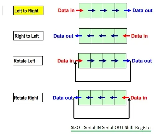
SISO 移位寄存器
Figure 1 illustrates a SISO shift register.
图 1 展示了 SISO 移位寄存器。
There are four types of SISO registers:
SISO 寄存器有四种类型:
-
Shift left without rotate
无循环左移
-
Shift right without rotate
无循环右移
-
Shift left with rotate
循环左移
-
Shift right with rotate
循环右移
In a right-shift SISO register, the Least Significant Bit (LSB) data is applied to the Most Significant Bit (MSB) flip-flop (e.g., a D flip-flop). SISO registers can introduce a delay equivalent to 'n' clock pulses to the input data. If 'T' is the time period of one clock pulse, the total delay provided by SISO is 'n*T'. In a left-shift SISO register, the MSB data is applied to the LSB flip-flop (D flip-flop).
在右移 SISO 寄存器中,最低有效位(LSB)数据会输入到最高有效位(MSB)触发器(例如 D 触发器)。SISO 寄存器可给输入数据引入相当于 n 个时钟脉冲的延迟:若单个时钟脉冲的周期为 T,则 SISO 提供的总延迟为 n × T n \times T n×T。在左移 SISO 寄存器中,MSB 数据会输入到 LSB 触发器(D 触发器)。
-
Clock pulses needed for input: n
输入所需时钟脉冲数: n
-
Clock pulses needed for output: n
输出所需时钟脉冲数:n
PIPO (Parallel In Parallel Out) Storage Register
PIPO(并行输入并行输出)存储寄存器
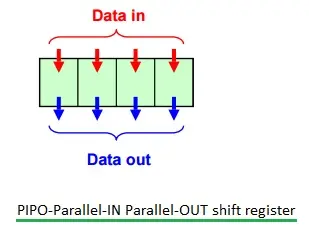
PIPO 移位寄存器
Figure 2 shows a PIPO register.
图 2 展示了 PIPO 寄存器。
The PIPO type is a storage register built from D flip-flops. It isn't strictly a shift register.
PIPO 类型是由 D 触发器构成的存储寄存器,并非严格意义上的移位寄存器。
-
Clock pulses needed for parallel input data: 1
并行输入数据所需时钟脉冲数: 1
-
Clock pulses needed for parallel output data: 0
并行输出数据所需时钟脉冲数: 0
SIPO (Serial In Parallel Out) Shift Register
SIPO(串行输入并行输出)移位寄存器
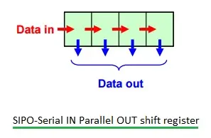
Figure 3 illustrates a SIPO shift register.
图 3 展示了 SIPO 移位寄存器。
-
For storing 'n' bits of serial input data, 'n' clock pulses are required.
存储 n 位串行输入数据需要 n 个时钟脉冲。
-
For storing 'n' bits of parallel output data, zero clock pulses are required, as no clock pulse is needed for this operation.
存储 n 位并行输出数据无需时钟脉冲,因此所需时钟脉冲数为 0。
-
Clock pulses needed for input: n
输入所需时钟脉冲数:n
-
Clock pulses needed for output: 0
输出所需时钟脉冲数:0
PISO (Parallel In Serial Out) Shift Register
PISO(并行输入串行输出)移位寄存器
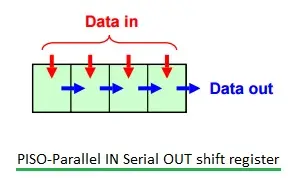
PISO 移位寄存器
Figure 4 illustrates a PISO shift register.
图 4 展示了 PISO 移位寄存器。
-
It is a parallel data storage register. To store 'n' bits, one clock pulse is needed.
它是并行数据存储寄存器,存储 n 位数据需要 1 个时钟脉冲。
-
To provide serial data as output, '(n-1)' clock pulses are needed.
输出串行数据需要 n − 1 n-1 n−1 个时钟脉冲。
-
Clock pulses needed for input: 1
输入所需时钟脉冲数:1
-
Clock pulses needed for output: n-1
输出所需时钟脉冲数: n − 1 n-1 n−1
Shift Registers -- Parallel & Serial -- PIPO, PISO, SISO, SIPO
移位寄存器------并行与串行:PIPO、PISO、SISO、SIPO
Umair Hussaini | Published October 16, 2018 | Updated April 19, 2024
In digital electronics, a collection of flip-flops, which are memory elements, is known as a register. Shift registers are special types of registers. Using shift registers, we can shift data through a series of flip-flops. In brief, shift registers are sequential logic circuits, where a series of flip-flops are connected together in a daisy chain configuration to shift digital data from one flip-flop to another with every clock cycle.
在数字电子学中,由触发器(存储元件)组成的集合被称为寄存器。移位寄存器是一类特殊的寄存器,借助它可以让数据在一系列触发器中移位。简而言之,移位寄存器是时序逻辑电路,其中多个触发器以菊花链结构连接,使得数字数据在每个时钟周期都会从一个触发器移至下一个触发器。
Shift registers are built using D flip-flops. If we connect four flip-flops in the configuration of a shift register, we get a 4-bit shift register. Generally, 8-bit (1 byte) shift registers are common. However, in this post, we will take a look at the different types of shift registers using only 4-bits or four flip-flops.
移位寄存器由D 触发器构成。若将 4 个触发器按移位寄存器的结构连接,就能得到 4 位移位寄存器。通常 8 位(1 字节)移位寄存器较为常见,但本文将以 4 位(即 4 个触发器)为例,介绍不同类型的移位寄存器。
How do shift registers move data?
移位寄存器如何传输数据?
We can feed and extract data to and from a shift register in two ways:
向移位寄存器输入数据和从其输出数据有两种方式:
- Serially: Data enters the cascade of flip-flops in a stream. Each bit passes through the cascade in a line. We get the data output at the last flip-flop. The output is in the same order as the input.
串行方式:数据以流的形式进入触发器级联结构,每一位按顺序通过级联电路,最终从最后一个触发器输出,输出顺序与输入顺序一致。 - Parallel: Each flip-flop can have its own input. This particular setting of giving input is known as parallel input. Similarly, each flip-flop can have its own output too. This is parallel output.
并行方式:每个触发器可单独输入数据,这种输入方式被称为并行输入;同理,每个触发器也可单独输出数据,这种输出方式被称为并行输出。
So we have two ways in which data can 'flow' through a shift register. We can classify shift registers depending on these two data flow methods. Doing that, we get four main configurations. The types of inputs and outputs of these four categories are evident from their names.
因此,数据在移位寄存器中有两种"流动"方式,我们可据此对移位寄存器分类,得到四种主要结构。这四类寄存器的输入输出类型可从其名称直接看出:
- Serial In Serial Out shift register
串行输入串行输出移位寄存器 - Serial In Parallel Out shift register
串行输入并行输出移位寄存器 - Parallel In Parallel Out shift register
并行输入并行输出移位寄存器 - Parallel In Serial Out shift register
并行输入串行输出移位寄存器
To quickly summarize a few things. Shift registers are a series of flip-flops connected together through which data shifts. They have four main types. The difference between these four types lies in the way we input and output data to/from them.
简言之,移位寄存器是由触发器级联而成、数据可在其中移位的电路,主要分为四类,区别在于数据的输入和输出方式。
Apart from inputs and outputs, shift registers also have a clock input and a reset signal. The reset signal clears the contents of all the flip-flops. Additionally, since the clock input is given to all the flip-flops simultaneously, shift registers are also synchronous circuits.
除输入输出端外,移位寄存器还包含时钟输入端和复位信号:复位信号用于清空所有触发器的内容;此外,由于时钟信号会同时输入所有触发器,移位寄存器属于同步电路。
What are the uses of shift registers?
移位寄存器的用途是什么?
Since a shift register comprises of flip-flops, we can use them for the following general purposes
由于移位寄存器由触发器组成,它可用于以下通用场景:
- To shift data -- Shift registers can shift data either to the right, to the left or in both directions. In this post, we will look at shift registers where the data moves in the right direction.
1数据移位------移位寄存器可实现数据的右移、左移或双向移位,本文将以数据右移的移位寄存器为例进行介绍。 - To store data -- The flip-flops shift data on the application of a clock pulse. In the absence of a clock pulse, the shift register holds that data.
数据存储------触发器在时钟脉冲作用下移位数据,无时钟脉冲时,移位寄存器会保持当前数据。 - To produce a delay -- The data can stay inside the shift register or pass through it. Either way, the processes consume some clock cycles. So we can use them to introduce some delay if we need it.
产生延迟------数据在移位寄存器中停留或传输会消耗若干时钟周期,因此可根据需求利用它引入延迟。 - To convert between serial-parallel -- Since we have both serial and parallel types of inputs and outputs, we can use shift registers to convert serial data to parallel or vice versa.
串并转换------借助串行和并行两种输入输出方式,移位寄存器可实现串行数据与并行数据的相互转换。
How to design a 4-bit Serial In Serial Out shift register (SISO)?
如何设计 4 位串行输入串行输出(SISO)移位寄存器?
Okay, so we know that we have four D flip-flops. All of them have the same clock input. And all of them have the same reset input. Since we have a serial input, we will take only one input port. This input port is to the first flip-flop in the register.
我们需要使用 4 个D 触发器,所有触发器共用同一时钟输入和复位输入。由于采用串行输入,只需设置一个输入端口,该端口连接到寄存器中的第一个触发器。
Similarly, since we are taking the output serially. We will have only one output which will be taken at the output pin of the last flip-flop. From the above configuration, our SISO shift register will look like this.
同理,由于采用串行输出,只需设置一个输出端口,该端口取自最后一个触发器的输出引脚。基于上述结构,我们的 SISO 移位寄存器构造如下。
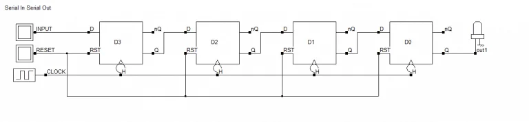
4-bit SISO shift register
4 位 SISO 移位寄存器
From the property of the D flip-flop, when we input a 1-bit signal "1", it will be present at D1 flip-flops output at the rising edge of the first clock cycle.
根据 D 触发器的特性,当输入 1 位信号"1"时,在第一个时钟周期的上升沿,该信号会出现在第一个 D 触发器(D1)的输出端。
In the next clock cycle it will be taken as input by the D2 flip-flop and will be available at Q2 output and so on. Furthermore, at the fourth clock pulse, we will get the 1-bit data "1" at the output Q4, having undergone a successful shift.
下一个时钟周期,该信号会作为第二个 D 触发器(D2)的输入,并出现在 Q2 输出端,以此类推。到第四个时钟脉冲时,1 位数据"1"会出现在 Q4 输出端,完成一次完整移位。
The timing diagram of data shift through a 4-bit SISO shift register
4 位 SISO 移位寄存器的数据移位时序图
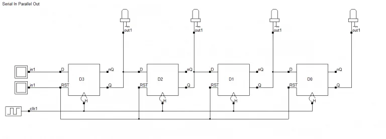
How to design a 4-bit Serial In Parallel Out shift register (SIPO)?
如何设计 4 位串行输入并行输出(SIPO)移位寄存器?
Let's take the four D flip-flops and take outputs from each individual flip-flop. That covers the parallel out part. Give a single input to the first flip-flop. Similarly, take a single output from the last flip-flop. Connect all the remaining flip-flops' outputs to their subsequent flip-flops' input. That settles the serial input part.
取 4 个 D 触发器,从每个触发器单独引出输出端,以此实现并行输出功能;给第一个触发器接入单个输入端口,将其余每个触发器的输出连接到下一个触发器的输入,以此实现串行输入功能。
Finally, apply the clock and the reset signal and voila you have your 4-bit SIPO shift register.
最后接入时钟信号和复位信号,这样就得到了 4 位 SIPO 移位寄存器。

4-bit SIPO shift register
4 位 SIPO 移位寄存器
How to design a 4-bit Parallel in Parallel Out shift register (PIPO)?
如何设计 4 位并行输入并行输出(PIPO)移位寄存器?
Again repeating the same approach we saw earlier, we will go ahead with cues from the title. Let's straightaway connect the output ports (Q ports) of the D flip-flops to the output pins. The name suggests that we have parallel inputs too. Hence, we will connect the input ports (D ports) of the flip-flops to the input pins.
延续之前的设计思路,我们从寄存器名称中获取设计线索。直接将 D 触发器的输出端(Q 端)连接到输出引脚;从名称可知该寄存器为并行输入,因此将每个触发器的输入端(D 端)连接到输入引脚。
Eventually, we will connect the clock ports to the clock input and the reset ports to the reset inputs. The resulting logic circuit for the 4-bit PIPO shift register is as follows.
最后将所有时钟端口接入时钟输入,所有复位端口接入复位输入,4 位 PIPO 移位寄存器的最终逻辑电路如下。
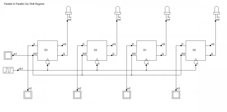
4-bit PIPO shift register
4 位 PIPO 移位寄存器
How to design a 4-bit Parallel in Serial Out shift register (PISO)?
如何设计 4 位并行输入串行输出(PISO)移位寄存器?
Things get a little bit tricky here. Mostly due to the fact that we need to share ports in order to achieve this configuration. The title requires us to have parallel inputs, which means that all the D ports will have their own independent input lines. And the title also requires us to have serial outputs.
这类寄存器的设计会稍复杂,主要原因是需要共享端口才能实现该结构。从名称可知,该寄存器需具备并行输入功能,这意味着所有 D 端都要有独立的输入线;同时它还需具备串行输出功能。
From the preceding designs, we have seen that a serial output means that data has to be taken out from only the final flip-flop. Moreover, the data needs to move through the series of flip-flops. This means that the outputs of flip-flops (Q ports) will also need to be connected to the inputs (D ports) of their subsequent flip-flops. This puts us in a pickle.
从之前的设计可知,串行输出意味着数据只能从最后一个触发器取出,而且数据需要在触发器级联中移位,这就要求触发器的输出端(Q 端)必须连接到下一个触发器的输入端(D 端)。这就产生了端口冲突的问题。
Dealing with multiple inputs
处理多输入问题
The input ports need their separate input line as well as a connection from the previous flip-flops. How can we give two distinct signals to the same port? What can we use that would allow us to select from one of the two inputs that need to be given to the flip-flops?
触发器的输入端口既需要独立的输入线,又需要与前一个触发器的输出相连。如何向同一个端口输入两个不同的信号?我们可以使用什么器件来选择需要输入到触发器的两个信号中的一个?
The answer is a multiplexer. A 2:1 multiplexer will allow us to choose between two inputs. So moving on to the construction of the PISO shift register. To begin with, let's connect all the clock inputs and reset signals to their respective inputs.
答案是使用多路选择器,2:1 多路选择器可实现二选一输入。接下来开始构建 PISO 移位寄存器:首先将所有时钟输入和复位信号接入对应的端口。
Then we know that we have a serial output so let's connect the output of the last flip-flop to the output pin. The first flip-flop also does not need a serial input because there is no preceding flip-flop. So let's give it its solitary input port. The remaining three flip-flops will have their inputs connected to the outputs of three multiplexers.
由于采用串行输出,将最后一个触发器的输出连接到输出引脚;第一个触发器没有前置触发器,因此无需串行输入,只需为其设置一个独立输入端口;剩余 3 个触发器的输入端分别连接到 3 个多路选择器的输出端。
Let's go ahead and make that connection. Now, the multiplexers have two inputs. The first is the independent input that we require because we are making a parallel input shift register. Second, the output of the preceding flip-flop since we need a serial shift of data to get a serial output.
接下来完成上述连接。每个多路选择器有两个输入信号:第一个是独立输入信号,用于实现并行输入功能;第二个是前一个触发器的输出信号,用于实现数据串行移位,进而实现串行输出功能。
The multiplexers also need a select input so that will be one extra input port. From the above configurations, we finally get a logic circuit for the 4-bit PISO shift register that looks like this.
多路选择器还需要一个选择输入端,这会作为寄存器的一个额外输入端口。基于上述结构,我们最终得到的 4 位 PISO 移位寄存器逻辑电路如下。
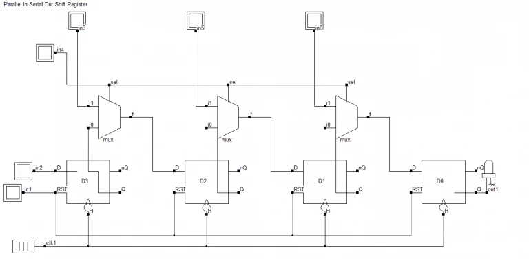
4-bit PISO shift register
4 位 PISO 移位寄存器
Some commonly available shift registers
常用的移位寄存器产品
Commonly available Shift Register ICs (source)
常用移位寄存器集成电路
Generally, shift registers are available in 4000 series and 7000 series ICs.
移位寄存器集成电路通常分为 4000 系列和 7000 系列。
4000 series
4000 系列
- IC 4006, 18 stage Shift register.
集成电路 4006:18 级移位寄存器 - IC 4014 8-stage shift register.
集成电路 4014:8 级移位寄存器 - IC 4015, Dual 4-stage shift register.
集成电路 4015:双 4 级移位寄存器 - IC 4021 8-bit static shift register.
集成电路 4021:8 位静态移位寄存器 - IC 40104 4 bit bidirectional Parallel-in/Parallel-out PIPO Shift Register.
- 集成电路 40104:4 位双向并行输入/并行输出(PIPO)移位寄存器
- IC 40195 4-bit universal shift register.
集成电路 40195:4 位通用移位寄存器
7000 series
7000 系列
- IC 7491 8-bit shift register, serial-in, serial-out, gated input.
集成电路 7491:8 位移位寄存器(串行输入、串行输出、门控输入) - IC 7495 4-bit shift register, parallel in, parallel-out, serial input.
集成电路 7495:4 位移位寄存器(并行输入、并行输出、串行输入) - IC 7496 5-bit parallel-In/parallel-out shift register, asynchronous preset.
集成电路 7496:5 位并行输入/并行输出移位寄存器(异步预置) - IC 7499 4-bit bidirectional universal shift register.
集成电路 7499:4 位双向通用移位寄存器 - IC 74164 8-bit parallel-out serial shift register with asynchronous.
集成电路 74164:8 位并行输出串行移位寄存器(带异步功能) - IC 74165 8-bit serial shift register, parallel Load, complementary outputs.
集成电路 74165:8 位串行移位寄存器(并行加载、互补输出) - IC 74166 parallel-Load 8-bit shift register.
集成电路 74166:并行加载 8 位移位寄存器 - IC 74194 4-bit bidirectional universal shift register.
集成电路 74194:4 位双向通用移位寄存器 - IC 74198 8-bit bidirectional universal shift register.
集成电路 74198:8 位双向通用移位寄存器 - IC 74199 8-bit bidirectional universal shift register with J-K serial inputs.
集成电路 74199:8 位双向通用移位寄存器(带 J-K 串行输入) - IC 74291 4-bit universal shift register, binary up/down counter, synchronous.
集成电路 74291:4 位通用移位寄存器(同步二进制加减计数器) - IC 74395 4-bit universal shift register with three-state outputs.
集成电路 74395:4 位通用移位寄存器(带三态输出) - IC 74498 8-bit bidirectional shift register with parallel inputs and three-state outputs.
集成电路 74498:8 位双向移位寄存器(带并行输入和三态输出) - IC 74671 4-bit bidirectional shift register.
集成电路 74671:4 位双向移位寄存器 - IC 74673 16-bit serial-in serial-out shift register with output storage registers.
集成电路 74673:16 位串行输入串行输出移位寄存器(带输出存储寄存器) - IC 74674 16-bit parallel-in serial-out shift register with three-state outputs.
集成电路 74674:16 位并行输入串行输出移位寄存器(带三态输出)
In these ICs, mostly used are
上述集成电路中,常用的型号包括:
- 74HC595 Serial-In-Parallel-Out shift register
74HC595:串行输入并行输出移位寄存器 - 74HC165 Parallel-In-Serial-Out shift register
74HC165:并行输入串行输出移位寄存器 - 74HC 194 4-bit bidirectional universal shift register
74HC194:4 位双向通用移位寄存器 - 74HC 198 8-bit bidirectional universal shift register
74HC198:8 位双向通用移位寄存器
via:
- SISO vs. SIPO vs. PISO vs. PIPO: Shift Register Types | RF Wireless World
https://www.rfwireless-world.com/terminology/siso-sipo-piso-pipo-shift-register-types - Shift Registers - Parallel & Serial - PIPO, PISO, SISO, SIPO
https://technobyte.org/shift-registers-parallel-serial-pipo-piso-siso-sipo/