OTA Specifications and Achieved value:
| Specifications | Value | Achieved | Unit | Satisified? (Yes/No) | |
|---|---|---|---|---|---|
| 1 | DC Gain | >70 | 72 | dB | Yes |
| 2 | GBW | >15 | 63 | MHz | Yes |
| 3 | Phase Margin | >65 | 68 | Degree | Yes |
| 4 | Input Offset Voltage | <5m | 2.17m | V | Yes |
| 5 | Input Common Mode Range | 0.1-1.2 | 0-1.2 | V | Yes |
| 6 | Output Common Mode Range | 0.3-1 | 0.072~1 | V | Yes |
| 7 | Supply Voltage | 1.2 | 1.2 | V | Yes |
| 8 | Power A/W | - | 37.3u/44.8u | A/W | - |
For the DC Gain, we also need two stages to achieve the target.
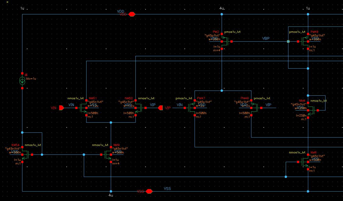
Given the supply voltage and input common-mode range, we need a rail-to-rail input amplifier.
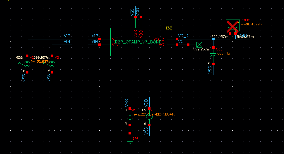
1) Offset Voltage Simulation
Use Unity gain buffer configuration to find the input offset voltage.
Monte-Carlo configuration

Simulation Result (Mean: 44u, std: 2.17m)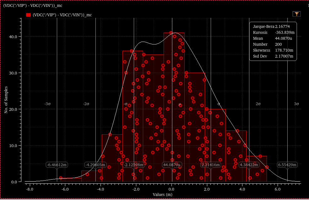
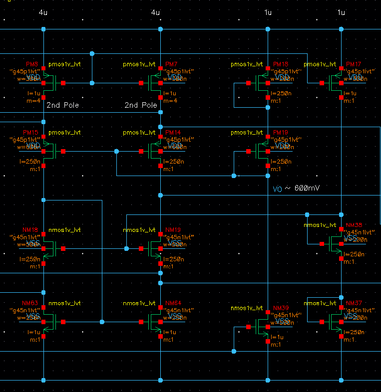
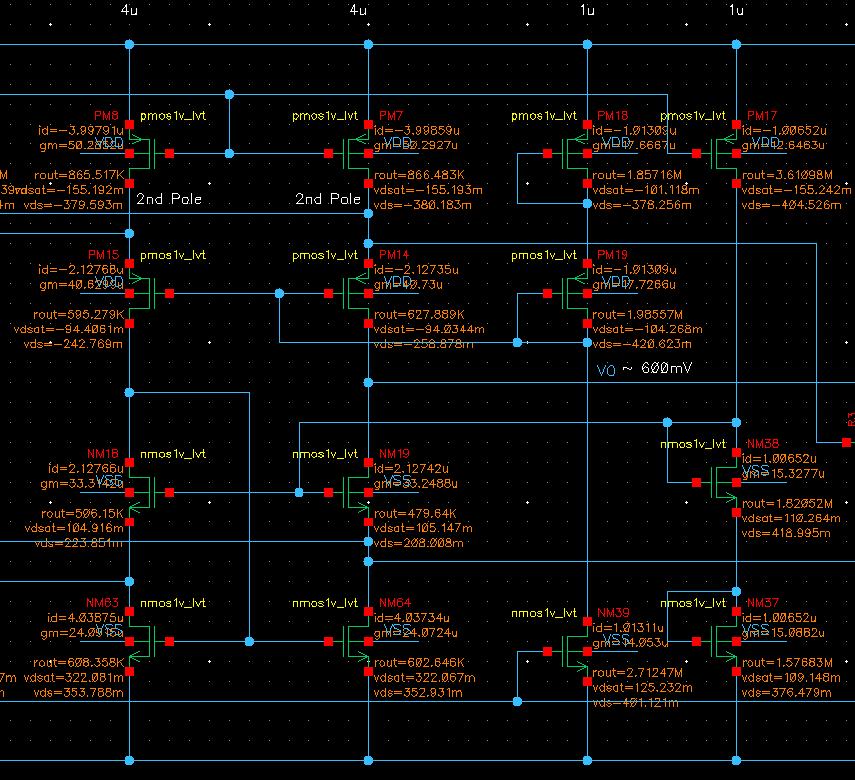
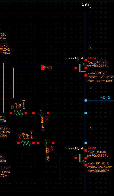
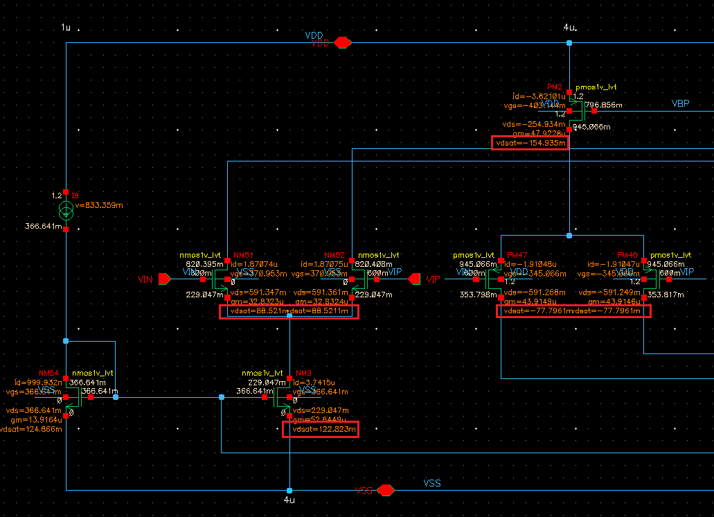
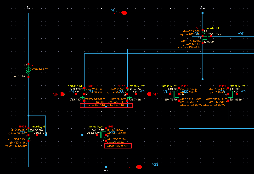
2) Schematic with transistor size
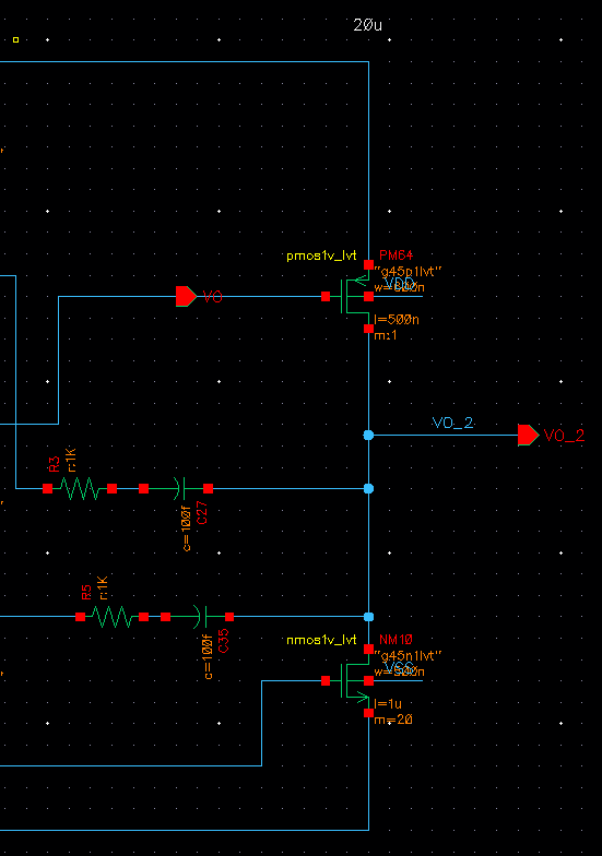
The Cc is 100fF for each
The Rc is 1kohm for each.
For miller compensation, connect Cc and Rc from output node to cascode nodes for better compensation.
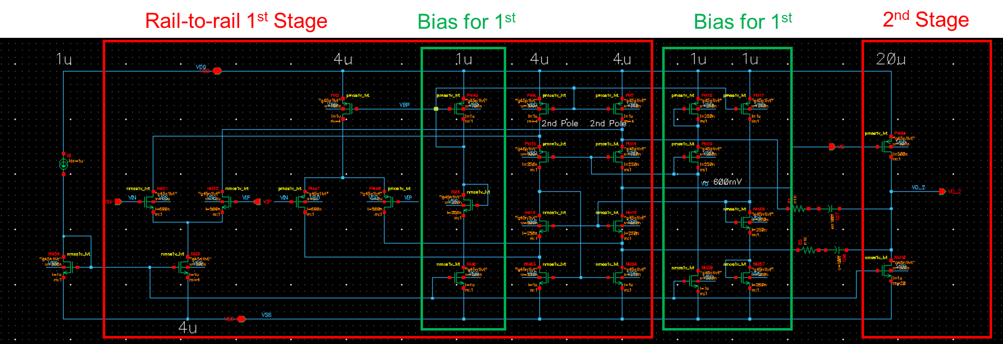
For detailed size, the figures are as shown below.
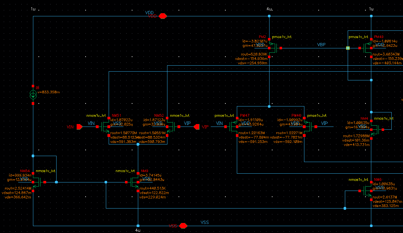
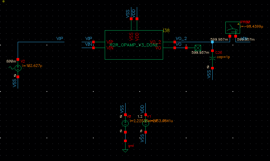
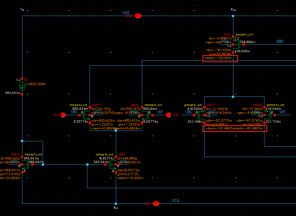
3) Schematic with DC Simulation
4) Performance Summary
Summary Table
| Specifications | Value | Achieved | Unit | |
|---|---|---|---|---|
| 1 | DC Gain | >70 | 72 | dB |
| 2 | GBW (1pF CLoadC_{Load}CLoad) | >15 | 63 | MHz |
| 3 | Phase Margin | >65 | 68 | Degree |
| 4 | Input Offset Voltage | <5m | 2.17m | V |
| 5 | Input Common Mode Range | 0.1-1.2 | 0-1.2 | V |
| 6 | Output Common Mode Range | 0.3-1 | 0.072~1 | V |
| 7 | Supply Voltage | 1.2 | 1.2 | V |
| 8 | Power A | - | 37.3u | A |
| 9 | Power W | - | 44.8u | W |
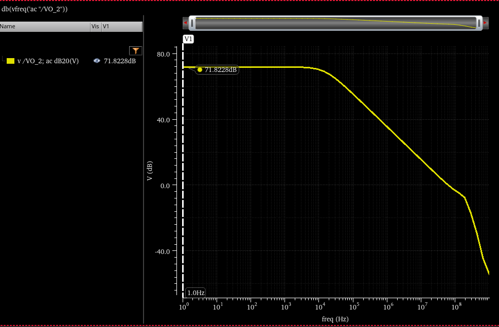
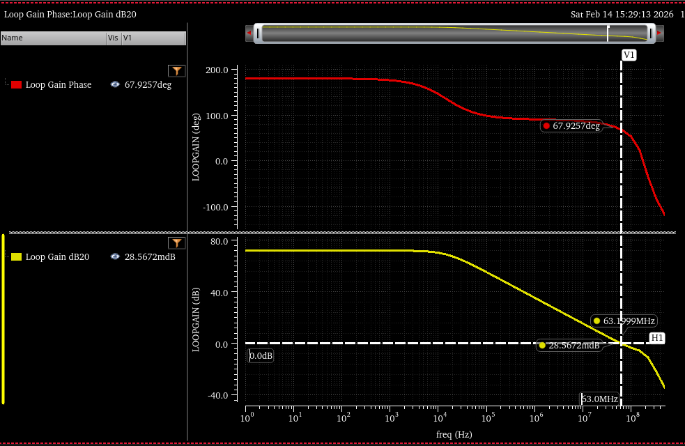
DC Gain 72-dB
- stb Simulation: 72-dB
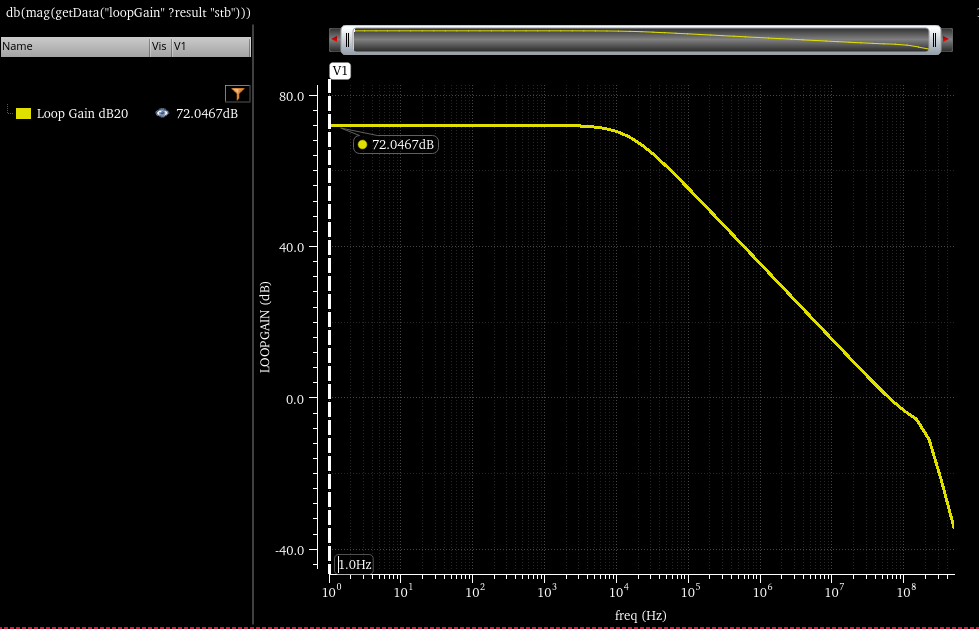
-
AC simulation: 72-dB
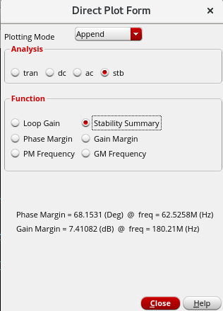
GBW 63-MHz (stb Simulation - Unity gain buffer configuration)
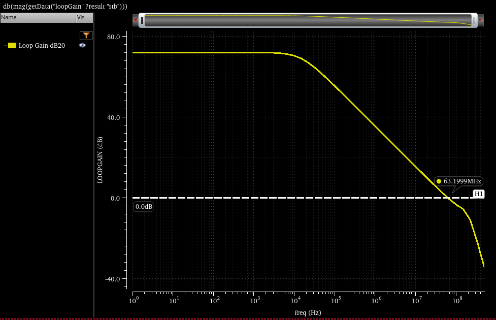
Phase Margin 68 degree (stb Simulation - Unity gain buffer configuration)
Input Offset Voltage ( VIP is vdc,600mV - Unity gain buffer configuration)

Monte-Carlo configuration
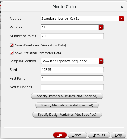
Simulation Result (Mean: 44u, std: 2.17m)

Input Common Mode Range (Based on Vdsat)
Because the input transistors is a pair of NMOS+PMOS, the Input common range is rail-to-rail, i.e. 0~1.2V.
- VCM:600mV
-
VCM:0
-
VCM:1.2V
-
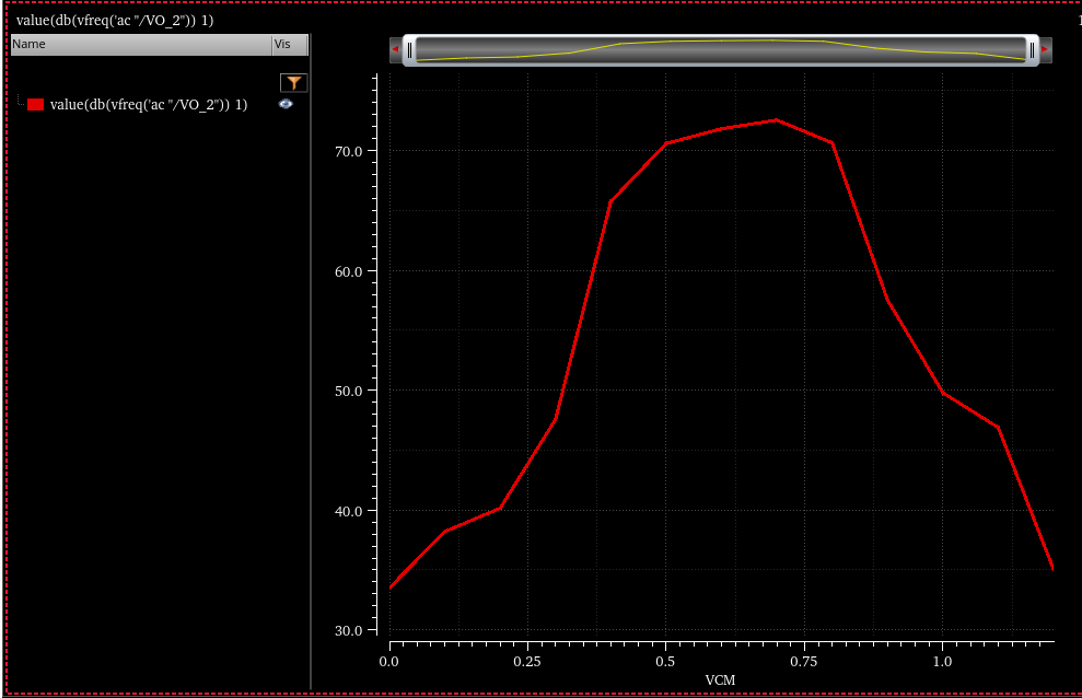
DC Gain VS VCM:
When Signal is closed to rail, only NMOS pair or PMOS pair is working, hence the total Gm is reduced compared with VCM=600mV.
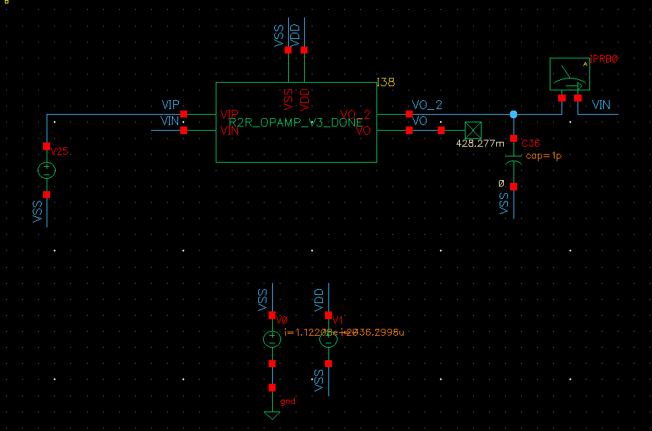
Ouput Common Mode Range (DC Simulation - Unity gain buffer configuration)
Sweep input signal at DC, and check whether the output can follow the input.
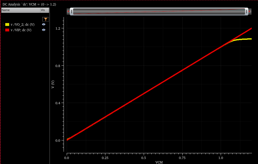
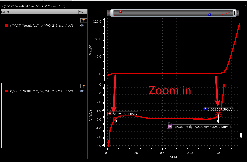
In the dc simulation result, we subtract the VIP and VIN, i.e. VIP-VO=VIP-VIN.
Then we can find the output common mode range: 72mV~1V
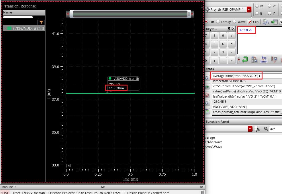
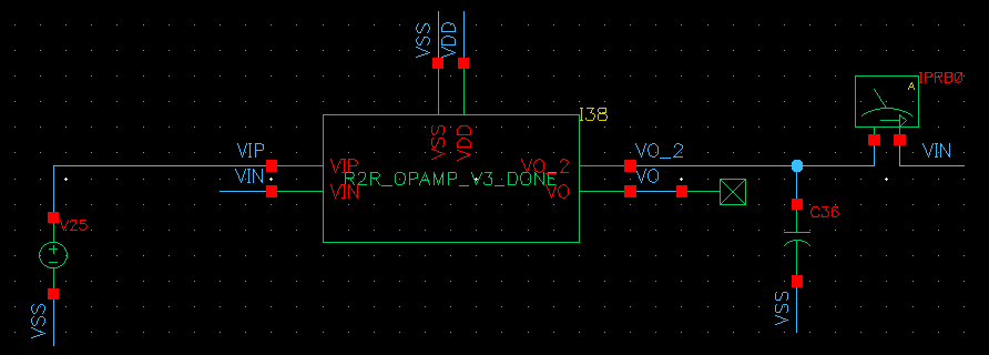
5) Current Consumption
Based on Unity gain buffer configuration, we can get the total current.
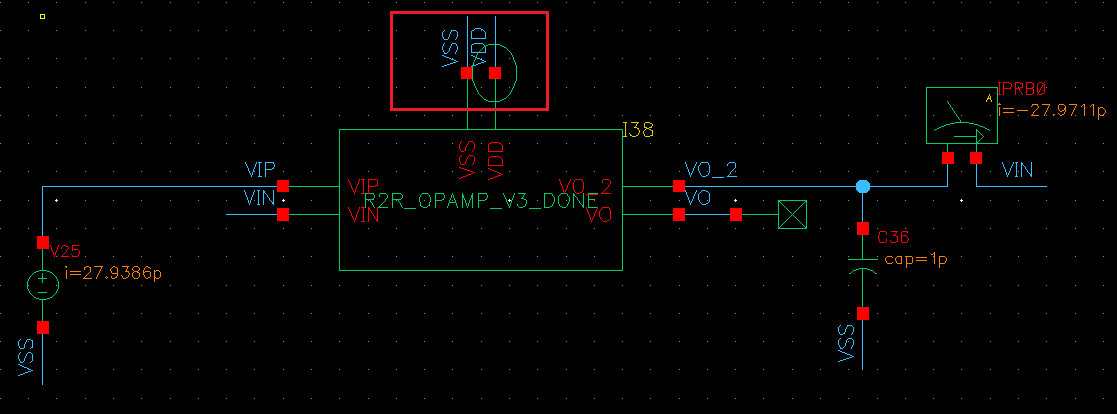
The average current value is 37.33uA. So the power is 37.33uA×1.2V=44.8uW37.33uA \times 1.2V = 44.8uW37.33uA×1.2V=44.8uW