封装AD9361接口IP核
-
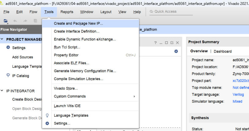
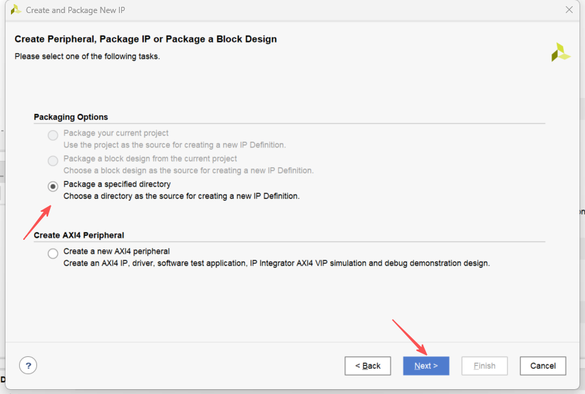
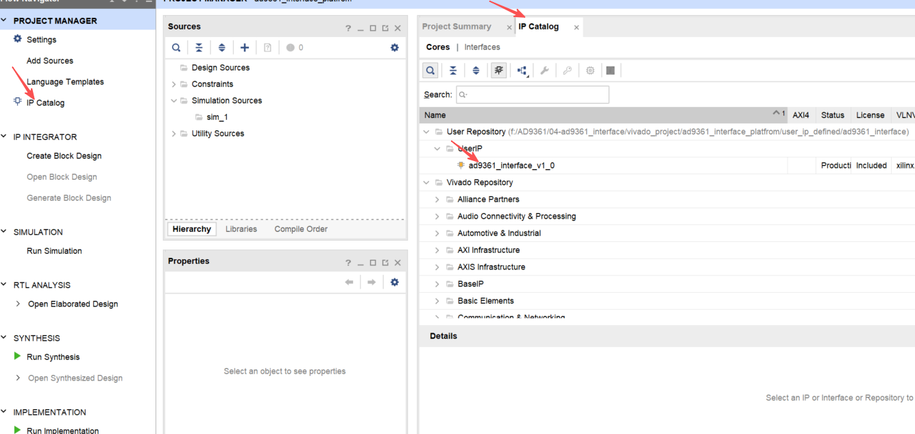
打开或创建一个Vivado工程,在菜单栏点击"Tools->Create and Package New IP..."打开创建或打包IP的向导。
-
点击"Nexit"

-
选择"Package a specified directory"
-
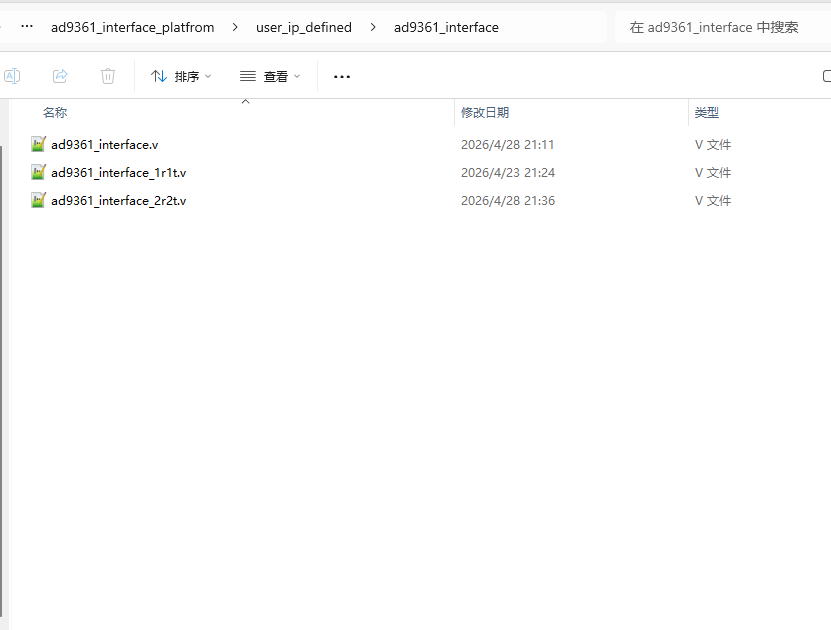
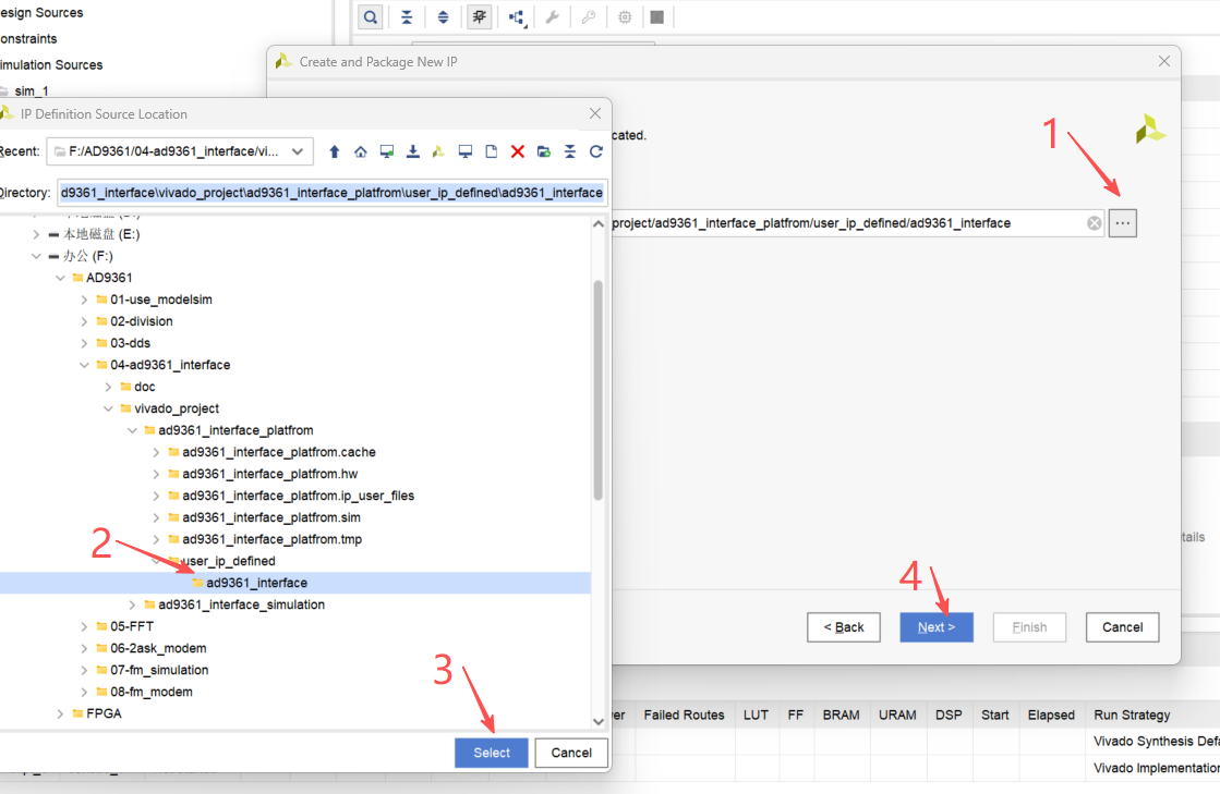
将06 AD9361 LVDS接口实现和仿真编写的代码复制到另一个目录(后面打包的IP核便在此目录),然后在向导中选择代码所在目录
-
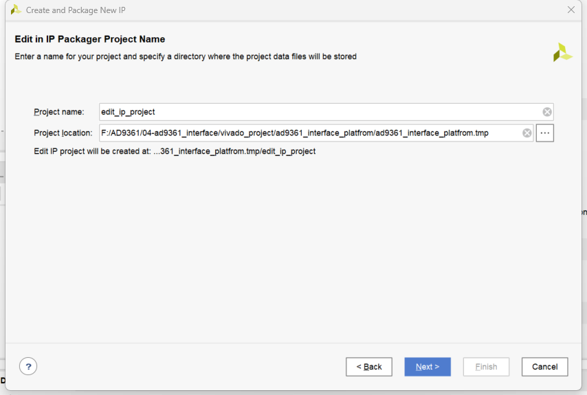
确定编辑IP的临时工程名称和路径,点击next
-
点击finish,打开编辑IP的临时工程
-
在临时工程的"Compatibility"中选择IP核支持的芯片
-
在临时工程的"Compatibility"中移除不需要支持的芯片(可以通过按住ctrl多选)
-
给"data_clk"增加"FREQ_HZ"属性,值设置为250M(因为AD9361时钟最大速率为245.76M,这里仅是告诉Vivado,后面这个时钟按250M处理)
-
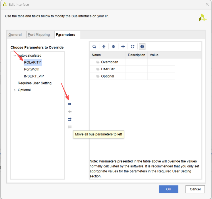
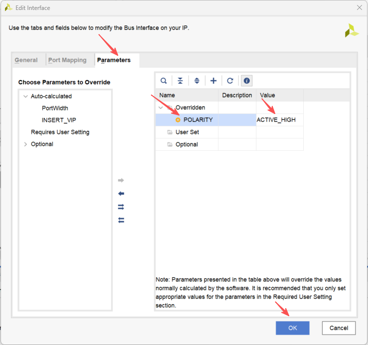
给"delay_cntrl_rst"添加复位极性属性,并设置为高电平复位
-
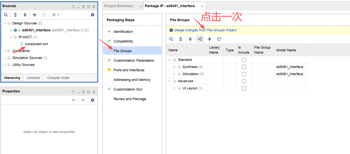
在临时工程的"File Groups"中更新文件变化
-
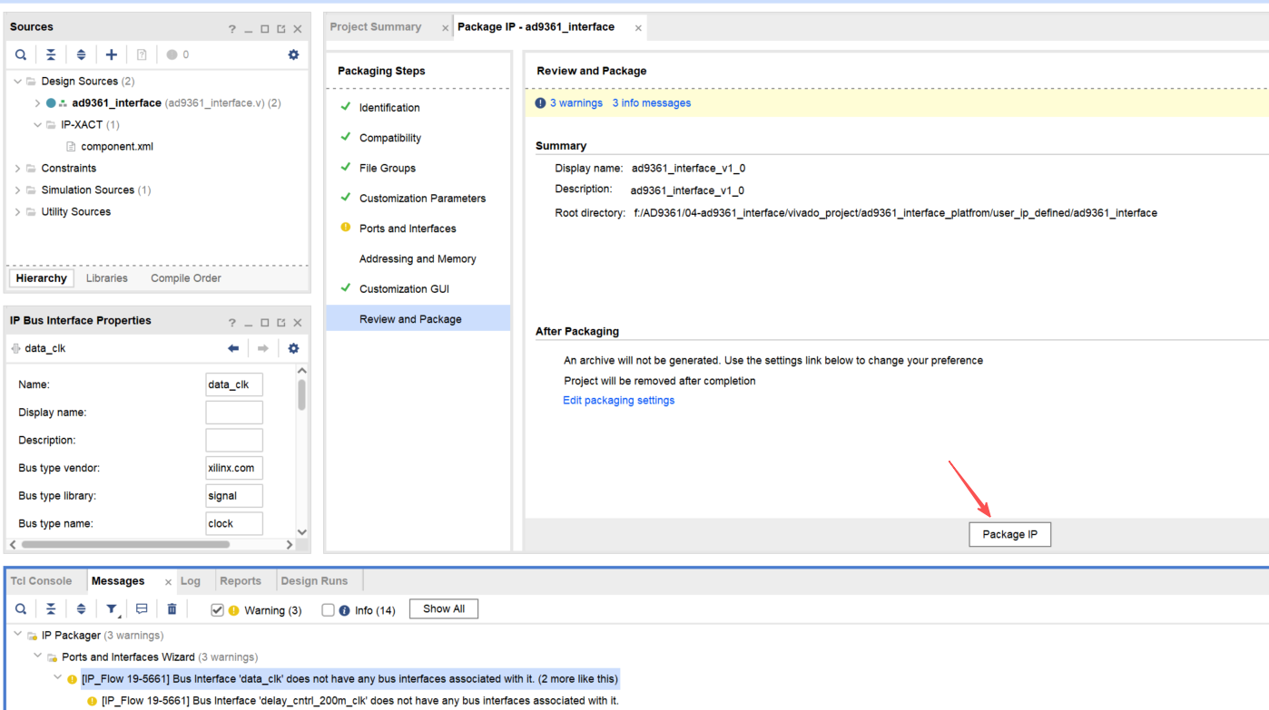
在临时工程的"Review and Package"点击打包IP
-
打包完成后会自动将IP核路径添加到父工程中
创建AD9361接口控制IP核
AD9361接口控制IP核用于通过AXI总线配置AD9361的IDELAY、使能data_clk等。
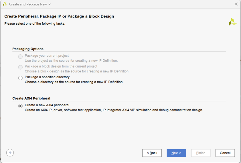
- 打开或创建一个Vivado工程,在菜单栏点击"Tools->Create and Package New IP..."打开创建或打包IP的向导。
- 点击"Nexit"
- 选择"Create a new AXl4 peripheral"
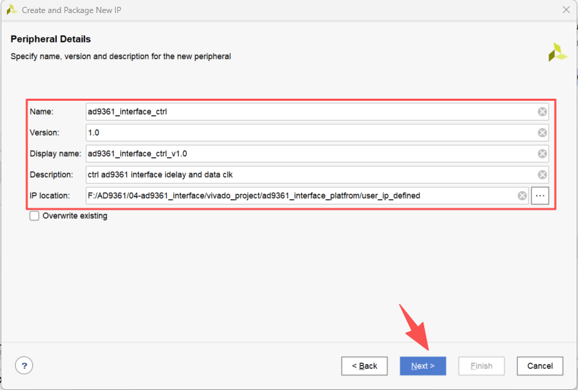
- 输入IP核名称、版本、描述信息等内容,选择IP存储路径
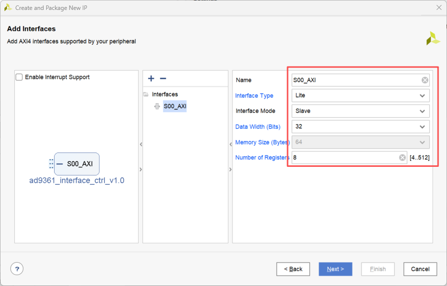
- 对默认添加的AXI接口进行配置,暂行设置为8个寄存器
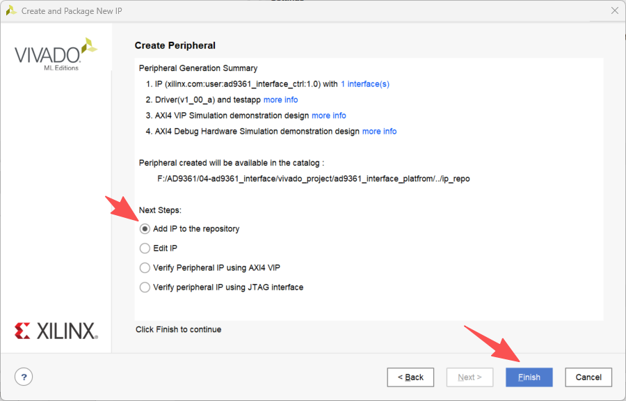
- 选择"Add IP to the repository",点击finish将IP添加到工程中
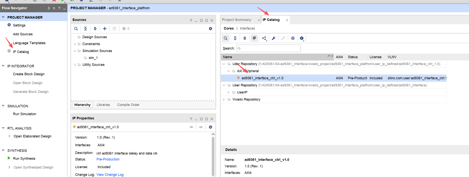
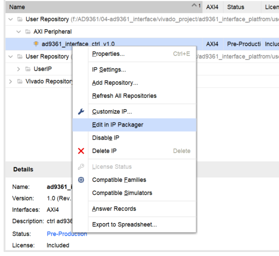
- 选中IP核,点击鼠标右键,选择"Edit in IP Packager",打开编辑IP核的临时工程,也可以在上一步中点击"Edit IP",然后在点击finish,这样可以一次性完成将IP添加到当前工程,并打开IP编辑临时工程
- 修改"ad9361_interface_ctrl_v1_0_S00_AXI.v"文件,增加IDELAY值输出接口、IDELAY值load接口、IDELAY锁定指示接口、data_clk使能接口,并将这些接口连接到AXI寄存器,修改后的内容如下:
c
`timescale 1 ns / 1 ps

	module ad9361_interface_ctrl_v1_0_S00_AXI #
	(
		// Users to add parameters here

		// User parameters ends
		// Do not modify the parameters beyond this line

		// Width of S_AXI data bus
		parameter integer C_S_AXI_DATA_WIDTH	= 32,
		// Width of S_AXI address bus
		parameter integer C_S_AXI_ADDR_WIDTH	= 5
	)
	(
		// Users to add ports here
		output reg  [6:0]  idelay_ld				,					//指示idelay_value作用于那个idelay,从0~6依次是rx_frame_in、rx_data_in[0]~rx_data_in[5]
		output reg  [4:0]  idelay_value				,					//idelay的延时参数
		input  wire        delay_cntrl_locked		,					//delay-cntrl锁定指示
		output reg         data_clk_ce				,					//使能数据参考时钟
		// User ports ends
		// Do not modify the ports beyond this line

		// Global Clock Signal
		input wire  S_AXI_ACLK,
		// Global Reset Signal. This Signal is Active LOW
		input wire  S_AXI_ARESETN,
		// Write address (issued by master, acceped by Slave)
		input wire [C_S_AXI_ADDR_WIDTH-1 : 0] S_AXI_AWADDR,
		// Write channel Protection type. This signal indicates the
    		// privilege and security level of the transaction, and whether
    		// the transaction is a data access or an instruction access.
		input wire [2 : 0] S_AXI_AWPROT,
		// Write address valid. This signal indicates that the master signaling
    		// valid write address and control information.
		input wire  S_AXI_AWVALID,
		// Write address ready. This signal indicates that the slave is ready
    		// to accept an address and associated control signals.
		output wire  S_AXI_AWREADY,
		// Write data (issued by master, acceped by Slave)
		input wire [C_S_AXI_DATA_WIDTH-1 : 0] S_AXI_WDATA,
		// Write strobes. This signal indicates which byte lanes hold
    		// valid data. There is one write strobe bit for each eight
    		// bits of the write data bus.
		input wire [(C_S_AXI_DATA_WIDTH/8)-1 : 0] S_AXI_WSTRB,
		// Write valid. This signal indicates that valid write
    		// data and strobes are available.
		input wire  S_AXI_WVALID,
		// Write ready. This signal indicates that the slave
    		// can accept the write data.
		output wire  S_AXI_WREADY,
		// Write response. This signal indicates the status
    		// of the write transaction.
		output wire [1 : 0] S_AXI_BRESP,
		// Write response valid. This signal indicates that the channel
    		// is signaling a valid write response.
		output wire  S_AXI_BVALID,
		// Response ready. This signal indicates that the master
    		// can accept a write response.
		input wire  S_AXI_BREADY,
		// Read address (issued by master, acceped by Slave)
		input wire [C_S_AXI_ADDR_WIDTH-1 : 0] S_AXI_ARADDR,
		// Protection type. This signal indicates the privilege
    		// and security level of the transaction, and whether the
    		// transaction is a data access or an instruction access.
		input wire [2 : 0] S_AXI_ARPROT,
		// Read address valid. This signal indicates that the channel
    		// is signaling valid read address and control information.
		input wire  S_AXI_ARVALID,
		// Read address ready. This signal indicates that the slave is
    		// ready to accept an address and associated control signals.
		output wire  S_AXI_ARREADY,
		// Read data (issued by slave)
		output wire [C_S_AXI_DATA_WIDTH-1 : 0] S_AXI_RDATA,
		// Read response. This signal indicates the status of the
    		// read transfer.
		output wire [1 : 0] S_AXI_RRESP,
		// Read valid. This signal indicates that the channel is
    		// signaling the required read data.
		output wire  S_AXI_RVALID,
		// Read ready. This signal indicates that the master can
    		// accept the read data and response information.
		input wire  S_AXI_RREADY
	);

	// AXI4LITE signals
	reg [C_S_AXI_ADDR_WIDTH-1 : 0] 	axi_awaddr;
	reg  	axi_awready;
	reg  	axi_wready;
	reg [1 : 0] 	axi_bresp;
	reg  	axi_bvalid;
	reg [C_S_AXI_ADDR_WIDTH-1 : 0] 	axi_araddr;
	reg  	axi_arready;
	reg [C_S_AXI_DATA_WIDTH-1 : 0] 	axi_rdata;
	reg [1 : 0] 	axi_rresp;
	reg  	axi_rvalid;

	// Example-specific design signals
	// local parameter for addressing 32 bit / 64 bit C_S_AXI_DATA_WIDTH
	// ADDR_LSB is used for addressing 32/64 bit registers/memories
	// ADDR_LSB = 2 for 32 bits (n downto 2)
	// ADDR_LSB = 3 for 64 bits (n downto 3)
	localparam integer ADDR_LSB = (C_S_AXI_DATA_WIDTH/32) + 1;
	localparam integer OPT_MEM_ADDR_BITS = 2;
	//----------------------------------------------
	//-- Signals for user logic register space example
	//------------------------------------------------
	//-- Number of Slave Registers 8
	reg [C_S_AXI_DATA_WIDTH-1:0]	slv_reg0;
	reg [C_S_AXI_DATA_WIDTH-1:0]	slv_reg1;
	reg [C_S_AXI_DATA_WIDTH-1:0]	slv_reg2;
	reg [C_S_AXI_DATA_WIDTH-1:0]	slv_reg3;
	reg [C_S_AXI_DATA_WIDTH-1:0]	slv_reg4;
	reg [C_S_AXI_DATA_WIDTH-1:0]	slv_reg5;
	reg [C_S_AXI_DATA_WIDTH-1:0]	slv_reg6;
	reg [C_S_AXI_DATA_WIDTH-1:0]	slv_reg7;
	wire	 slv_reg_rden;
	wire	 slv_reg_wren;
	reg [C_S_AXI_DATA_WIDTH-1:0]	 reg_data_out;
	integer	 byte_index;
	reg	 aw_en;

	// I/O Connections assignments

	assign S_AXI_AWREADY	= axi_awready;
	assign S_AXI_WREADY	= axi_wready;
	assign S_AXI_BRESP	= axi_bresp;
	assign S_AXI_BVALID	= axi_bvalid;
	assign S_AXI_ARREADY	= axi_arready;
	assign S_AXI_RDATA	= axi_rdata;
	assign S_AXI_RRESP	= axi_rresp;
	assign S_AXI_RVALID	= axi_rvalid;
	// Implement axi_awready generation
	// axi_awready is asserted for one S_AXI_ACLK clock cycle when both
	// S_AXI_AWVALID and S_AXI_WVALID are asserted. axi_awready is
	// de-asserted when reset is low.

	always @( posedge S_AXI_ACLK )
	begin
	  if ( S_AXI_ARESETN == 1'b0 )
	    begin
	      axi_awready <= 1'b0;
	      aw_en <= 1'b1;
	    end
	  else
	    begin
	      if (~axi_awready && S_AXI_AWVALID && S_AXI_WVALID && aw_en)
	        begin
	          // slave is ready to accept write address when
	          // there is a valid write address and write data
	          // on the write address and data bus. This design
	          // expects no outstanding transactions.
	          axi_awready <= 1'b1;
	          aw_en <= 1'b0;
	        end
	        else if (S_AXI_BREADY && axi_bvalid)
	            begin
	              aw_en <= 1'b1;
	              axi_awready <= 1'b0;
	            end
	      else
	        begin
	          axi_awready <= 1'b0;
	        end
	    end
	end

	// Implement axi_awaddr latching
	// This process is used to latch the address when both
	// S_AXI_AWVALID and S_AXI_WVALID are valid.

	always @( posedge S_AXI_ACLK )
	begin
	  if ( S_AXI_ARESETN == 1'b0 )
	    begin
	      axi_awaddr <= 0;
	    end
	  else
	    begin
	      if (~axi_awready && S_AXI_AWVALID && S_AXI_WVALID && aw_en)
	        begin
	          // Write Address latching
	          axi_awaddr <= S_AXI_AWADDR;
	        end
	    end
	end

	// Implement axi_wready generation
	// axi_wready is asserted for one S_AXI_ACLK clock cycle when both
	// S_AXI_AWVALID and S_AXI_WVALID are asserted. axi_wready is
	// de-asserted when reset is low.

	always @( posedge S_AXI_ACLK )
	begin
	  if ( S_AXI_ARESETN == 1'b0 )
	    begin
	      axi_wready <= 1'b0;
	    end
	  else
	    begin
	      if (~axi_wready && S_AXI_WVALID && S_AXI_AWVALID && aw_en )
	        begin
	          // slave is ready to accept write data when
	          // there is a valid write address and write data
	          // on the write address and data bus. This design
	          // expects no outstanding transactions.
	          axi_wready <= 1'b1;
	        end
	      else
	        begin
	          axi_wready <= 1'b0;
	        end
	    end
	end

	// Implement memory mapped register select and write logic generation
	// The write data is accepted and written to memory mapped registers when
	// axi_awready, S_AXI_WVALID, axi_wready and S_AXI_WVALID are asserted. Write strobes are used to
	// select byte enables of slave registers while writing.
	// These registers are cleared when reset (active low) is applied.
	// Slave register write enable is asserted when valid address and data are available
	// and the slave is ready to accept the write address and write data.
	assign slv_reg_wren = axi_wready && S_AXI_WVALID && axi_awready && S_AXI_AWVALID;

	always @( posedge S_AXI_ACLK )
	begin
	  if ( S_AXI_ARESETN == 1'b0 )
	    begin
	      slv_reg0 <= 0;
	      slv_reg1 <= 0;
//	      slv_reg2 <= 0;
	      slv_reg3 <= 0;
	      slv_reg4 <= 0;
	      slv_reg5 <= 0;
	      slv_reg6 <= 0;
	      slv_reg7 <= 0;
	    end
	  else begin
	    if (slv_reg_wren)
	      begin
	        case ( axi_awaddr[ADDR_LSB+OPT_MEM_ADDR_BITS:ADDR_LSB] )
	          3'h0:
	            for ( byte_index = 0; byte_index <= (C_S_AXI_DATA_WIDTH/8)-1; byte_index = byte_index+1 )
	              if ( S_AXI_WSTRB[byte_index] == 1 ) begin
	                // Respective byte enables are asserted as per write strobes
	                // Slave register 0
	                slv_reg0[(byte_index*8) +: 8] <= S_AXI_WDATA[(byte_index*8) +: 8];
	              end
	          3'h1:
	            for ( byte_index = 0; byte_index <= (C_S_AXI_DATA_WIDTH/8)-1; byte_index = byte_index+1 )
	              if ( S_AXI_WSTRB[byte_index] == 1 ) begin
	                // Respective byte enables are asserted as per write strobes
	                // Slave register 1
	                slv_reg1[(byte_index*8) +: 8] <= S_AXI_WDATA[(byte_index*8) +: 8];
	              end
//	          3'h2:
//	            for ( byte_index = 0; byte_index <= (C_S_AXI_DATA_WIDTH/8)-1; byte_index = byte_index+1 )
//	              if ( S_AXI_WSTRB[byte_index] == 1 ) begin
//	                // Respective byte enables are asserted as per write strobes
//	                // Slave register 2
//	                slv_reg2[(byte_index*8) +: 8] <= S_AXI_WDATA[(byte_index*8) +: 8];
//	              end
	          3'h3:
	            for ( byte_index = 0; byte_index <= (C_S_AXI_DATA_WIDTH/8)-1; byte_index = byte_index+1 )
	              if ( S_AXI_WSTRB[byte_index] == 1 ) begin
	                // Respective byte enables are asserted as per write strobes
	                // Slave register 3
	                slv_reg3[(byte_index*8) +: 8] <= S_AXI_WDATA[(byte_index*8) +: 8];
	              end
	          3'h4:
	            for ( byte_index = 0; byte_index <= (C_S_AXI_DATA_WIDTH/8)-1; byte_index = byte_index+1 )
	              if ( S_AXI_WSTRB[byte_index] == 1 ) begin
	                // Respective byte enables are asserted as per write strobes
	                // Slave register 4
	                slv_reg4[(byte_index*8) +: 8] <= S_AXI_WDATA[(byte_index*8) +: 8];
	              end
	          3'h5:
	            for ( byte_index = 0; byte_index <= (C_S_AXI_DATA_WIDTH/8)-1; byte_index = byte_index+1 )
	              if ( S_AXI_WSTRB[byte_index] == 1 ) begin
	                // Respective byte enables are asserted as per write strobes
	                // Slave register 5
	                slv_reg5[(byte_index*8) +: 8] <= S_AXI_WDATA[(byte_index*8) +: 8];
	              end
	          3'h6:
	            for ( byte_index = 0; byte_index <= (C_S_AXI_DATA_WIDTH/8)-1; byte_index = byte_index+1 )
	              if ( S_AXI_WSTRB[byte_index] == 1 ) begin
	                // Respective byte enables are asserted as per write strobes
	                // Slave register 6
	                slv_reg6[(byte_index*8) +: 8] <= S_AXI_WDATA[(byte_index*8) +: 8];
	              end
	          3'h7:
	            for ( byte_index = 0; byte_index <= (C_S_AXI_DATA_WIDTH/8)-1; byte_index = byte_index+1 )
	              if ( S_AXI_WSTRB[byte_index] == 1 ) begin
	                // Respective byte enables are asserted as per write strobes
	                // Slave register 7
	                slv_reg7[(byte_index*8) +: 8] <= S_AXI_WDATA[(byte_index*8) +: 8];
	              end
	          default : begin
	                      slv_reg0 <= slv_reg0;
	                      slv_reg1 <= slv_reg1;
//	                      slv_reg2 <= slv_reg2;
	                      slv_reg3 <= slv_reg3;
	                      slv_reg4 <= slv_reg4;
	                      slv_reg5 <= slv_reg5;
	                      slv_reg6 <= slv_reg6;
	                      slv_reg7 <= slv_reg7;
	                    end
	        endcase
	      end
	  end
	end

	// Implement write response logic generation
	// The write response and response valid signals are asserted by the slave
	// when axi_wready, S_AXI_WVALID, axi_wready and S_AXI_WVALID are asserted.
	// This marks the acceptance of address and indicates the status of
	// write transaction.

	always @( posedge S_AXI_ACLK )
	begin
	  if ( S_AXI_ARESETN == 1'b0 )
	    begin
	      axi_bvalid  <= 0;
	      axi_bresp   <= 2'b0;
	    end
	  else
	    begin
	      if (axi_awready && S_AXI_AWVALID && ~axi_bvalid && axi_wready && S_AXI_WVALID)
	        begin
	          // indicates a valid write response is available
	          axi_bvalid <= 1'b1;
	          axi_bresp  <= 2'b0; // 'OKAY' response
	        end                   // work error responses in future
	      else
	        begin
	          if (S_AXI_BREADY && axi_bvalid)
	            //check if bready is asserted while bvalid is high)
	            //(there is a possibility that bready is always asserted high)
	            begin
	              axi_bvalid <= 1'b0;
	            end
	        end
	    end
	end

	// Implement axi_arready generation
	// axi_arready is asserted for one S_AXI_ACLK clock cycle when
	// S_AXI_ARVALID is asserted. axi_awready is
	// de-asserted when reset (active low) is asserted.
	// The read address is also latched when S_AXI_ARVALID is
	// asserted. axi_araddr is reset to zero on reset assertion.

	always @( posedge S_AXI_ACLK )
	begin
	  if ( S_AXI_ARESETN == 1'b0 )
	    begin
	      axi_arready <= 1'b0;
	      axi_araddr  <= 32'b0;
	    end
	  else
	    begin
	      if (~axi_arready && S_AXI_ARVALID)
	        begin
	          // indicates that the slave has acceped the valid read address
	          axi_arready <= 1'b1;
	          // Read address latching
	          axi_araddr  <= S_AXI_ARADDR;
	        end
	      else
	        begin
	          axi_arready <= 1'b0;
	        end
	    end
	end

	// Implement axi_arvalid generation
	// axi_rvalid is asserted for one S_AXI_ACLK clock cycle when both
	// S_AXI_ARVALID and axi_arready are asserted. The slave registers
	// data are available on the axi_rdata bus at this instance. The
	// assertion of axi_rvalid marks the validity of read data on the
	// bus and axi_rresp indicates the status of read transaction.axi_rvalid
	// is deasserted on reset (active low). axi_rresp and axi_rdata are
	// cleared to zero on reset (active low).
	always @( posedge S_AXI_ACLK )
	begin
	  if ( S_AXI_ARESETN == 1'b0 )
	    begin
	      axi_rvalid <= 0;
	      axi_rresp  <= 0;
	    end
	  else
	    begin
	      if (axi_arready && S_AXI_ARVALID && ~axi_rvalid)
	        begin
	          // Valid read data is available at the read data bus
	          axi_rvalid <= 1'b1;
	          axi_rresp  <= 2'b0; // 'OKAY' response
	        end
	      else if (axi_rvalid && S_AXI_RREADY)
	        begin
	          // Read data is accepted by the master
	          axi_rvalid <= 1'b0;
	        end
	    end
	end

	// Implement memory mapped register select and read logic generation
	// Slave register read enable is asserted when valid address is available
	// and the slave is ready to accept the read address.
	assign slv_reg_rden = axi_arready & S_AXI_ARVALID & ~axi_rvalid;
	always @(*)
	begin
	      // Address decoding for reading registers
	      case ( axi_araddr[ADDR_LSB+OPT_MEM_ADDR_BITS:ADDR_LSB] )
	        3'h0   : reg_data_out <= slv_reg0;
	        3'h1   : reg_data_out <= slv_reg1;
	        3'h2   : reg_data_out <= slv_reg2;
	        3'h3   : reg_data_out <= slv_reg3;
	        3'h4   : reg_data_out <= slv_reg4;
	        3'h5   : reg_data_out <= slv_reg5;
	        3'h6   : reg_data_out <= slv_reg6;
	        3'h7   : reg_data_out <= slv_reg7;
	        default : reg_data_out <= 0;
	      endcase
	end

	// Output register or memory read data
	always @( posedge S_AXI_ACLK )
	begin
	  if ( S_AXI_ARESETN == 1'b0 )
	    begin
	      axi_rdata  <= 0;
	    end
	  else
	    begin
	      // When there is a valid read address (S_AXI_ARVALID) with
	      // acceptance of read address by the slave (axi_arready),
	      // output the read dada
	      if (slv_reg_rden)
	        begin
	          axi_rdata <= reg_data_out;     // register read data
	        end
	    end
	end

	// Add user logic here
	//指示idelay_value作用于那个idelay,从0~6依次是rx_frame_in、rx_data_in[0]~rx_data_in[5]
	always @( posedge S_AXI_ACLK ) begin
		if ( S_AXI_ARESETN == 1'b0 )
			idelay_ld <= 7'b0;
		else
			idelay_ld <= slv_reg0[6:0];
	end
	//idelay的延时参数
	always @( posedge S_AXI_ACLK ) begin
		if ( S_AXI_ARESETN == 1'b0 )
			idelay_value <= 5'b0;
		else
			idelay_value <= slv_reg1[4:0];
	end
	//delay-cntrl锁定指示
	always @( posedge S_AXI_ACLK ) begin
		if ( S_AXI_ARESETN == 1'b0 )
			slv_reg2 <= 32'b0;
		else
			slv_reg2 <= {31'b0, delay_cntrl_locked};
	end
	//使能数据参考时钟
	always @( posedge S_AXI_ACLK ) begin
		if ( S_AXI_ARESETN == 1'b0 )
			data_clk_ce <= 15'b0;
		else
			data_clk_ce <= slv_reg3[0];
	end
	// User logic ends

endmodule- 相应的寄存器功能定义如下:
c
寄存器定义
	名称            地址             索引            读写       描述
	slv_reg0         0(0x000)         0(0x000)       [wr]       指示idelay延时参数作用于那个idelay,从0~6依次是rx_frame_in、rx_data_in[0]~rx_data_in[5]
	slv_reg1         4(0x004)         1(0x001)       [wr]       idelay的延时参数
	slv_reg2        16(0x010)         4(0x004)       [r]        delay-cntrl锁定指示
slv_reg3 20(0x014) 5(0x005) [wr] 使能数据参考时钟data_clk- 修改"ad9361_interface_ctrl_v1_0.v"文件,将"ad9361_interface_ctrl_v1_0_S00_AXI.v"文件增加的信号引出到IP核外部,修改后的内容如下:
c
`timescale 1 ns / 1 ps

	module ad9361_interface_ctrl_v1_0 #
	(
		// Users to add parameters here

		// User parameters ends
		// Do not modify the parameters beyond this line


		// Parameters of Axi Slave Bus Interface S00_AXI
		parameter integer C_S00_AXI_DATA_WIDTH	= 32,
		parameter integer C_S00_AXI_ADDR_WIDTH	= 5
	)
	(
		// Users to add ports here
		output wire [6:0]  idelay_ld				,					//指示idelay_value作用于那个idelay,从0~6依次是rx_frame_in、rx_data_in[0]~rx_data_in[5]
		output wire [4:0]  idelay_value				,					//idelay的延时参数
		input  wire        delay_cntrl_locked		,					//delay-cntrl锁定指示
		output wire        data_clk_ce				,					//使能数据参考时钟
		// User ports ends
		// Do not modify the ports beyond this line


		// Ports of Axi Slave Bus Interface S00_AXI
		input wire  s00_axi_aclk,
		input wire  s00_axi_aresetn,
		input wire [C_S00_AXI_ADDR_WIDTH-1 : 0] s00_axi_awaddr,
		input wire [2 : 0] s00_axi_awprot,
		input wire  s00_axi_awvalid,
		output wire  s00_axi_awready,
		input wire [C_S00_AXI_DATA_WIDTH-1 : 0] s00_axi_wdata,
		input wire [(C_S00_AXI_DATA_WIDTH/8)-1 : 0] s00_axi_wstrb,
		input wire  s00_axi_wvalid,
		output wire  s00_axi_wready,
		output wire [1 : 0] s00_axi_bresp,
		output wire  s00_axi_bvalid,
		input wire  s00_axi_bready,
		input wire [C_S00_AXI_ADDR_WIDTH-1 : 0] s00_axi_araddr,
		input wire [2 : 0] s00_axi_arprot,
		input wire  s00_axi_arvalid,
		output wire  s00_axi_arready,
		output wire [C_S00_AXI_DATA_WIDTH-1 : 0] s00_axi_rdata,
		output wire [1 : 0] s00_axi_rresp,
		output wire  s00_axi_rvalid,
		input wire  s00_axi_rready
	);
// Instantiation of Axi Bus Interface S00_AXI
	ad9361_interface_ctrl_v1_0_S00_AXI # (
		.C_S_AXI_DATA_WIDTH(C_S00_AXI_DATA_WIDTH),
		.C_S_AXI_ADDR_WIDTH(C_S00_AXI_ADDR_WIDTH)
	) ad9361_interface_ctrl_v1_0_S00_AXI_inst (
		.idelay_ld(idelay_ld),							//指示idelay_value作用于那个idelay,从0~6依次是rx_frame_in、rx_data_in[0]~rx_data_in[5]
		.idelay_value(idelay_value),					//idelay的延时参数
		.delay_cntrl_locked(delay_cntrl_locked),		//delay-cntrl锁定指示
		.data_clk_ce(data_clk_ce),						//使能数据参考时钟
		.S_AXI_ACLK(s00_axi_aclk),
		.S_AXI_ARESETN(s00_axi_aresetn),
		.S_AXI_AWADDR(s00_axi_awaddr),
		.S_AXI_AWPROT(s00_axi_awprot),
		.S_AXI_AWVALID(s00_axi_awvalid),
		.S_AXI_AWREADY(s00_axi_awready),
		.S_AXI_WDATA(s00_axi_wdata),
		.S_AXI_WSTRB(s00_axi_wstrb),
		.S_AXI_WVALID(s00_axi_wvalid),
		.S_AXI_WREADY(s00_axi_wready),
		.S_AXI_BRESP(s00_axi_bresp),
		.S_AXI_BVALID(s00_axi_bvalid),
		.S_AXI_BREADY(s00_axi_bready),
		.S_AXI_ARADDR(s00_axi_araddr),
		.S_AXI_ARPROT(s00_axi_arprot),
		.S_AXI_ARVALID(s00_axi_arvalid),
		.S_AXI_ARREADY(s00_axi_arready),
		.S_AXI_RDATA(s00_axi_rdata),
		.S_AXI_RRESP(s00_axi_rresp),
		.S_AXI_RVALID(s00_axi_rvalid),
		.S_AXI_RREADY(s00_axi_rready)
	);

	// Add user logic here

	// User logic ends
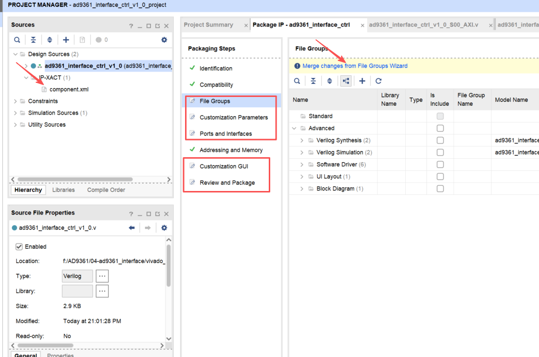
endmodule- 依次在临时工程"Compatibility.xml"的File Groups、Customization Parameters、Customzation GUI、Review and Package中更新文件改变。
完成后显示如下:
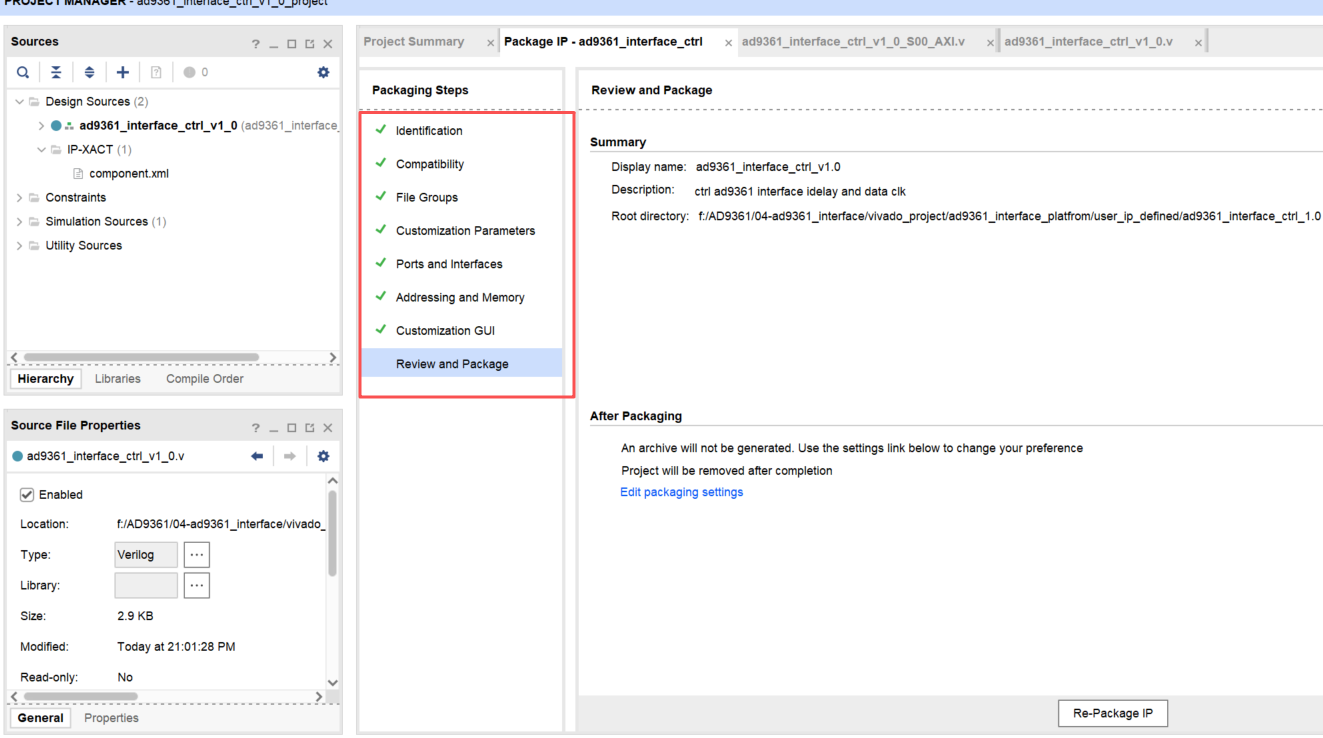
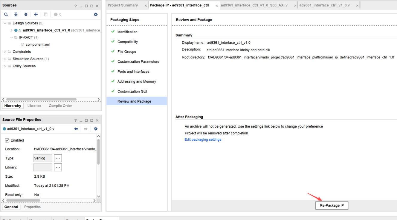
- 依次在临时工程"Compatibility.xml"的Review and Package中点击Re-Package IP,进行重新打包。
创建AD9361数据生成IP核
AD9361数据生成IP核利用DDS信号发生器根据AD9361的时钟和DAC数据速率生成余弦信号(I路)和正弦信号(Q路),用于AD9361 DAC部分的激励源。
- 按照"创建AD9361接口控制IP核"中的步骤1到7创建一个名为ad9361_data_generate的IP核,并打开编辑IP的临时工程。
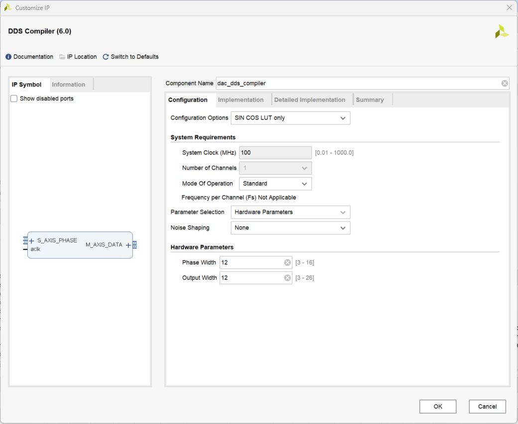
- 在临时工程中添加一个DDS IP核
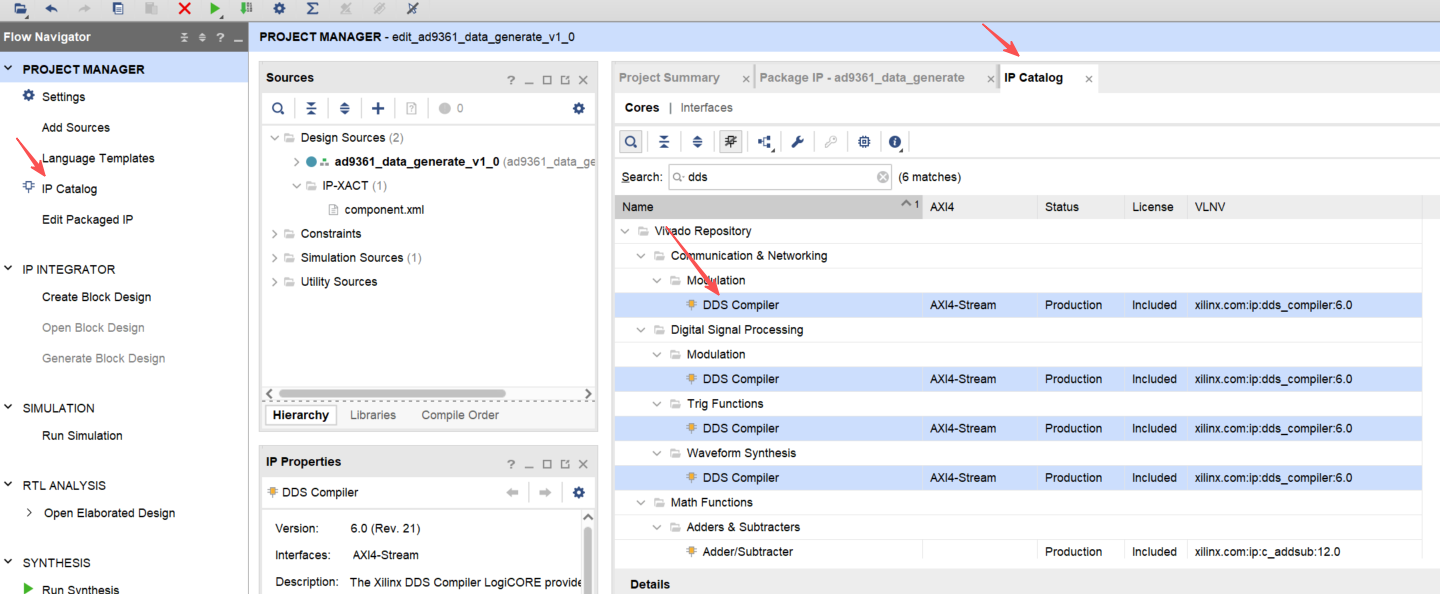
IP核配置如下:
- 创建文件"dac_data_generate.v",文件路径建议选择IP核中的hdl或src目录,文件内容如下所示:
c
`timescale 1 ns / 1 ps

module dac_data_generate #(
	parameter          MODE_1R1T = 0
)
(
	//复位信号
	input  wire        sys_rst_n				,
	//DAC 数据参考时钟
	input  wire        sys_clk					,
	//相位步进
	input  wire [15:0] phase_step				,
	//DAC IQ数据
	output reg         dac_data_valid			,					//DAC数据流效标志
	output reg  [15:0] dac_data_i1				,					//DAC CH1数据
	output reg  [15:0] dac_data_q1				,
	output reg  [15:0] dac_data_i2				,					//DAC CH2数据
	output reg  [15:0] dac_data_q2
);

//DDS信号发生器相位控制字
reg         phase_tvalid = 1'b0;
reg  [15:0] phase_tdata = 16'b0;

//DDS信号发生器输出数据
wire        dds_data_tvalid;
wire [31:0] dds_data_tdata;

//相位步间隔进计数器
reg  [1:0]  interval_count = 2'b0;

//相位步进间隔计数,计数器溢出清零,1R1T模式只使用bit[0],2R2T使用bit[1:0]
always @(posedge sys_clk) begin
	if(!sys_rst_n)
		interval_count <= 2'b0;
	else
		interval_count <= interval_count + 2'b1;
end

generate
	if(MODE_1R1T == 1) begin
		//1R1T模式下每两个时钟周期相位步进一次,所以在interval_count[0] == 1'b1时相位有效
		always @(posedge sys_clk) begin
			if(!sys_rst_n)
				phase_tvalid <= 1'b0;
			else if(interval_count[0] == 1'b1)
				phase_tvalid <= 1'b1;
			else
				phase_tvalid <= 1'b0;
		end

		//相位加一个步进,为下一次做准备
		always @(posedge sys_clk) begin
			if(!sys_rst_n)
				phase_tdata <= 16'b0;
			else if(phase_tvalid == 1'b1)
				phase_tdata <= phase_tdata + phase_step;
		end

		//DDS数据输出,1R1T模式下只有CH1有数据
		always @(posedge sys_clk) begin
			if(!sys_rst_n) begin
				dac_data_valid <= 1'b0;
				dac_data_i1 <= 16'b0;
				dac_data_q1 <= 16'b0;
				dac_data_i2 <= 16'b0;
				dac_data_q2 <= 16'b0;
			end
			else begin
				dac_data_valid <= dds_data_tvalid;
				dac_data_i1 <= dds_data_tdata[27:16];
				dac_data_q1 <= dds_data_tdata[11:0];
				dac_data_i2 <= 16'b0;
				dac_data_q2 <= 16'b0;
			end
		end
	end
	else begin
		//2R2T模式下每四个时钟周期相位步进一次,所以在interval_count[1:0] == 2'b11时相位有效
		always @(posedge sys_clk) begin
			if(!sys_rst_n)
				phase_tvalid <= 1'b0;
			else if(interval_count[1:0] == 2'b11)
				phase_tvalid <= 1'b1;
			else
				phase_tvalid <= 1'b0;
		end

		//相位加一个步进,为下一次做准备
		always @(posedge sys_clk) begin
			if(!sys_rst_n)
				phase_tdata <= 16'b0;
			else if(phase_tvalid == 1'b1)
				phase_tdata <= phase_tdata + phase_step;
		end

		//DDS数据输出,2R2T模式下CH1和CH2均有数据
		always @(posedge sys_clk) begin
			if(!sys_rst_n) begin
				dac_data_valid <= 1'b0;
				dac_data_i1 <= 16'b0;
				dac_data_q1 <= 16'b0;
				dac_data_i2 <= 16'b0;
				dac_data_q2 <= 16'b0;
			end
			else begin
				dac_data_valid <= dds_data_tvalid;
				dac_data_i1 <= {{4{dds_data_tdata[27]}}, dds_data_tdata[27:16]};
				dac_data_q1 <= {{4{dds_data_tdata[11]}}, dds_data_tdata[11:0]};
				dac_data_i2 <= {{4{dds_data_tdata[27]}}, dds_data_tdata[27:16]};
				dac_data_q2 <= {{4{dds_data_tdata[11]}}, dds_data_tdata[11:0]};
			end
		end
	end
endgenerate

//DDS信号发生器
dac_dds_compiler u_dac_dds_compiler_inst0(
	.aclk(sys_clk),
	.s_axis_phase_tvalid(phase_tvalid),
	.s_axis_phase_tdata(phase_tdata),
	.m_axis_data_tvalid(dds_data_tvalid),
	.m_axis_data_tdata(dds_data_tdata)
);

endmodule- 修改"ad9361_data_generate_v1_0_S00_AXI.v",例化dac_data_generate,并增加对dac_data_generate的控制,修改后的内容如下所示:
c
`timescale 1 ns / 1 ps

	module ad9361_data_generate_v1_0_S00_AXI #
	(
		// Users to add parameters here
		parameter          MODE_1R1T = 0,
		// User parameters ends
		// Do not modify the parameters beyond this line

		// Width of S_AXI data bus
		parameter integer C_S_AXI_DATA_WIDTH	= 32,
		// Width of S_AXI address bus
		parameter integer C_S_AXI_ADDR_WIDTH	= 5
	)
	(
		// Users to add ports here
		//DAC 数据参考时钟
		input  wire        data_clk					,					//数据参考时钟
		//DAC IQ数据
		output wire        dac_data_valid			,					//DAC数据流效标志
		output wire [15:0] dac_data_i1				,					//DAC CH1数据
		output wire [15:0] dac_data_q1				,
		output wire [15:0] dac_data_i2				,					//DAC CH2数据
		output wire [15:0] dac_data_q2				,
		// User ports ends
		// Do not modify the ports beyond this line

		// Global Clock Signal
		input wire  S_AXI_ACLK,
		// Global Reset Signal. This Signal is Active LOW
		input wire  S_AXI_ARESETN,
		// Write address (issued by master, acceped by Slave)
		input wire [C_S_AXI_ADDR_WIDTH-1 : 0] S_AXI_AWADDR,
		// Write channel Protection type. This signal indicates the
    		// privilege and security level of the transaction, and whether
    		// the transaction is a data access or an instruction access.
		input wire [2 : 0] S_AXI_AWPROT,
		// Write address valid. This signal indicates that the master signaling
    		// valid write address and control information.
		input wire  S_AXI_AWVALID,
		// Write address ready. This signal indicates that the slave is ready
    		// to accept an address and associated control signals.
		output wire  S_AXI_AWREADY,
		// Write data (issued by master, acceped by Slave)
		input wire [C_S_AXI_DATA_WIDTH-1 : 0] S_AXI_WDATA,
		// Write strobes. This signal indicates which byte lanes hold
    		// valid data. There is one write strobe bit for each eight
    		// bits of the write data bus.
		input wire [(C_S_AXI_DATA_WIDTH/8)-1 : 0] S_AXI_WSTRB,
		// Write valid. This signal indicates that valid write
    		// data and strobes are available.
		input wire  S_AXI_WVALID,
		// Write ready. This signal indicates that the slave
    		// can accept the write data.
		output wire  S_AXI_WREADY,
		// Write response. This signal indicates the status
    		// of the write transaction.
		output wire [1 : 0] S_AXI_BRESP,
		// Write response valid. This signal indicates that the channel
    		// is signaling a valid write response.
		output wire  S_AXI_BVALID,
		// Response ready. This signal indicates that the master
    		// can accept a write response.
		input wire  S_AXI_BREADY,
		// Read address (issued by master, acceped by Slave)
		input wire [C_S_AXI_ADDR_WIDTH-1 : 0] S_AXI_ARADDR,
		// Protection type. This signal indicates the privilege
    		// and security level of the transaction, and whether the
    		// transaction is a data access or an instruction access.
		input wire [2 : 0] S_AXI_ARPROT,
		// Read address valid. This signal indicates that the channel
    		// is signaling valid read address and control information.
		input wire  S_AXI_ARVALID,
		// Read address ready. This signal indicates that the slave is
    		// ready to accept an address and associated control signals.
		output wire  S_AXI_ARREADY,
		// Read data (issued by slave)
		output wire [C_S_AXI_DATA_WIDTH-1 : 0] S_AXI_RDATA,
		// Read response. This signal indicates the status of the
    		// read transfer.
		output wire [1 : 0] S_AXI_RRESP,
		// Read valid. This signal indicates that the channel is
    		// signaling the required read data.
		output wire  S_AXI_RVALID,
		// Read ready. This signal indicates that the master can
    		// accept the read data and response information.
		input wire  S_AXI_RREADY
	);

	// AXI4LITE signals
	reg [C_S_AXI_ADDR_WIDTH-1 : 0] 	axi_awaddr;
	reg  	axi_awready;
	reg  	axi_wready;
	reg [1 : 0] 	axi_bresp;
	reg  	axi_bvalid;
	reg [C_S_AXI_ADDR_WIDTH-1 : 0] 	axi_araddr;
	reg  	axi_arready;
	reg [C_S_AXI_DATA_WIDTH-1 : 0] 	axi_rdata;
	reg [1 : 0] 	axi_rresp;
	reg  	axi_rvalid;

	// Example-specific design signals
	// local parameter for addressing 32 bit / 64 bit C_S_AXI_DATA_WIDTH
	// ADDR_LSB is used for addressing 32/64 bit registers/memories
	// ADDR_LSB = 2 for 32 bits (n downto 2)
	// ADDR_LSB = 3 for 64 bits (n downto 3)
	localparam integer ADDR_LSB = (C_S_AXI_DATA_WIDTH/32) + 1;
	localparam integer OPT_MEM_ADDR_BITS = 2;
	//----------------------------------------------
	//-- Signals for user logic register space example
	//------------------------------------------------
	//-- Number of Slave Registers 8
	reg [C_S_AXI_DATA_WIDTH-1:0]	slv_reg0;
	reg [C_S_AXI_DATA_WIDTH-1:0]	slv_reg1;
	reg [C_S_AXI_DATA_WIDTH-1:0]	slv_reg2;
	reg [C_S_AXI_DATA_WIDTH-1:0]	slv_reg3;
	reg [C_S_AXI_DATA_WIDTH-1:0]	slv_reg4;
	reg [C_S_AXI_DATA_WIDTH-1:0]	slv_reg5;
	reg [C_S_AXI_DATA_WIDTH-1:0]	slv_reg6;
	reg [C_S_AXI_DATA_WIDTH-1:0]	slv_reg7;
	wire	 slv_reg_rden;
	wire	 slv_reg_wren;
	reg [C_S_AXI_DATA_WIDTH-1:0]	 reg_data_out;
	integer	 byte_index;
	reg	 aw_en;

	//通过XPMCDC同步到data_clk时钟域的控制信号,bit[16]使能控制,bit[15:0]相位步进
	wire [16:0] data_clk_ctrl_single;

	// I/O Connections assignments

	assign S_AXI_AWREADY	= axi_awready;
	assign S_AXI_WREADY	= axi_wready;
	assign S_AXI_BRESP	= axi_bresp;
	assign S_AXI_BVALID	= axi_bvalid;
	assign S_AXI_ARREADY	= axi_arready;
	assign S_AXI_RDATA	= axi_rdata;
	assign S_AXI_RRESP	= axi_rresp;
	assign S_AXI_RVALID	= axi_rvalid;
	// Implement axi_awready generation
	// axi_awready is asserted for one S_AXI_ACLK clock cycle when both
	// S_AXI_AWVALID and S_AXI_WVALID are asserted. axi_awready is
	// de-asserted when reset is low.

	always @( posedge S_AXI_ACLK )
	begin
	  if ( S_AXI_ARESETN == 1'b0 )
	    begin
	      axi_awready <= 1'b0;
	      aw_en <= 1'b1;
	    end
	  else
	    begin
	      if (~axi_awready && S_AXI_AWVALID && S_AXI_WVALID && aw_en)
	        begin
	          // slave is ready to accept write address when
	          // there is a valid write address and write data
	          // on the write address and data bus. This design
	          // expects no outstanding transactions.
	          axi_awready <= 1'b1;
	          aw_en <= 1'b0;
	        end
	        else if (S_AXI_BREADY && axi_bvalid)
	            begin
	              aw_en <= 1'b1;
	              axi_awready <= 1'b0;
	            end
	      else
	        begin
	          axi_awready <= 1'b0;
	        end
	    end
	end

	// Implement axi_awaddr latching
	// This process is used to latch the address when both
	// S_AXI_AWVALID and S_AXI_WVALID are valid.

	always @( posedge S_AXI_ACLK )
	begin
	  if ( S_AXI_ARESETN == 1'b0 )
	    begin
	      axi_awaddr <= 0;
	    end
	  else
	    begin
	      if (~axi_awready && S_AXI_AWVALID && S_AXI_WVALID && aw_en)
	        begin
	          // Write Address latching
	          axi_awaddr <= S_AXI_AWADDR;
	        end
	    end
	end

	// Implement axi_wready generation
	// axi_wready is asserted for one S_AXI_ACLK clock cycle when both
	// S_AXI_AWVALID and S_AXI_WVALID are asserted. axi_wready is
	// de-asserted when reset is low.

	always @( posedge S_AXI_ACLK )
	begin
	  if ( S_AXI_ARESETN == 1'b0 )
	    begin
	      axi_wready <= 1'b0;
	    end
	  else
	    begin
	      if (~axi_wready && S_AXI_WVALID && S_AXI_AWVALID && aw_en )
	        begin
	          // slave is ready to accept write data when
	          // there is a valid write address and write data
	          // on the write address and data bus. This design
	          // expects no outstanding transactions.
	          axi_wready <= 1'b1;
	        end
	      else
	        begin
	          axi_wready <= 1'b0;
	        end
	    end
	end

	// Implement memory mapped register select and write logic generation
	// The write data is accepted and written to memory mapped registers when
	// axi_awready, S_AXI_WVALID, axi_wready and S_AXI_WVALID are asserted. Write strobes are used to
	// select byte enables of slave registers while writing.
	// These registers are cleared when reset (active low) is applied.
	// Slave register write enable is asserted when valid address and data are available
	// and the slave is ready to accept the write address and write data.
	assign slv_reg_wren = axi_wready && S_AXI_WVALID && axi_awready && S_AXI_AWVALID;

	always @( posedge S_AXI_ACLK )
	begin
	  if ( S_AXI_ARESETN == 1'b0 )
	    begin
	      slv_reg0 <= 0;
	      slv_reg1 <= 0;
	      slv_reg2 <= 0;
	      slv_reg3 <= 0;
	      slv_reg4 <= 0;
	      slv_reg5 <= 0;
	      slv_reg6 <= 0;
	      slv_reg7 <= 0;
	    end
	  else begin
	    if (slv_reg_wren)
	      begin
	        case ( axi_awaddr[ADDR_LSB+OPT_MEM_ADDR_BITS:ADDR_LSB] )
	          3'h0:
	            for ( byte_index = 0; byte_index <= (C_S_AXI_DATA_WIDTH/8)-1; byte_index = byte_index+1 )
	              if ( S_AXI_WSTRB[byte_index] == 1 ) begin
	                // Respective byte enables are asserted as per write strobes
	                // Slave register 0
	                slv_reg0[(byte_index*8) +: 8] <= S_AXI_WDATA[(byte_index*8) +: 8];
	              end
	          3'h1:
	            for ( byte_index = 0; byte_index <= (C_S_AXI_DATA_WIDTH/8)-1; byte_index = byte_index+1 )
	              if ( S_AXI_WSTRB[byte_index] == 1 ) begin
	                // Respective byte enables are asserted as per write strobes
	                // Slave register 1
	                slv_reg1[(byte_index*8) +: 8] <= S_AXI_WDATA[(byte_index*8) +: 8];
	              end
	          3'h2:
	            for ( byte_index = 0; byte_index <= (C_S_AXI_DATA_WIDTH/8)-1; byte_index = byte_index+1 )
	              if ( S_AXI_WSTRB[byte_index] == 1 ) begin
	                // Respective byte enables are asserted as per write strobes
	                // Slave register 2
	                slv_reg2[(byte_index*8) +: 8] <= S_AXI_WDATA[(byte_index*8) +: 8];
	              end
	          3'h3:
	            for ( byte_index = 0; byte_index <= (C_S_AXI_DATA_WIDTH/8)-1; byte_index = byte_index+1 )
	              if ( S_AXI_WSTRB[byte_index] == 1 ) begin
	                // Respective byte enables are asserted as per write strobes
	                // Slave register 3
	                slv_reg3[(byte_index*8) +: 8] <= S_AXI_WDATA[(byte_index*8) +: 8];
	              end
	          3'h4:
	            for ( byte_index = 0; byte_index <= (C_S_AXI_DATA_WIDTH/8)-1; byte_index = byte_index+1 )
	              if ( S_AXI_WSTRB[byte_index] == 1 ) begin
	                // Respective byte enables are asserted as per write strobes
	                // Slave register 4
	                slv_reg4[(byte_index*8) +: 8] <= S_AXI_WDATA[(byte_index*8) +: 8];
	              end
	          3'h5:
	            for ( byte_index = 0; byte_index <= (C_S_AXI_DATA_WIDTH/8)-1; byte_index = byte_index+1 )
	              if ( S_AXI_WSTRB[byte_index] == 1 ) begin
	                // Respective byte enables are asserted as per write strobes
	                // Slave register 5
	                slv_reg5[(byte_index*8) +: 8] <= S_AXI_WDATA[(byte_index*8) +: 8];
	              end
	          3'h6:
	            for ( byte_index = 0; byte_index <= (C_S_AXI_DATA_WIDTH/8)-1; byte_index = byte_index+1 )
	              if ( S_AXI_WSTRB[byte_index] == 1 ) begin
	                // Respective byte enables are asserted as per write strobes
	                // Slave register 6
	                slv_reg6[(byte_index*8) +: 8] <= S_AXI_WDATA[(byte_index*8) +: 8];
	              end
	          3'h7:
	            for ( byte_index = 0; byte_index <= (C_S_AXI_DATA_WIDTH/8)-1; byte_index = byte_index+1 )
	              if ( S_AXI_WSTRB[byte_index] == 1 ) begin
	                // Respective byte enables are asserted as per write strobes
	                // Slave register 7
	                slv_reg7[(byte_index*8) +: 8] <= S_AXI_WDATA[(byte_index*8) +: 8];
	              end
	          default : begin
	                      slv_reg0 <= slv_reg0;
	                      slv_reg1 <= slv_reg1;
	                      slv_reg2 <= slv_reg2;
	                      slv_reg3 <= slv_reg3;
	                      slv_reg4 <= slv_reg4;
	                      slv_reg5 <= slv_reg5;
	                      slv_reg6 <= slv_reg6;
	                      slv_reg7 <= slv_reg7;
	                    end
	        endcase
	      end
	  end
	end

	// Implement write response logic generation
	// The write response and response valid signals are asserted by the slave
	// when axi_wready, S_AXI_WVALID, axi_wready and S_AXI_WVALID are asserted.
	// This marks the acceptance of address and indicates the status of
	// write transaction.

	always @( posedge S_AXI_ACLK )
	begin
	  if ( S_AXI_ARESETN == 1'b0 )
	    begin
	      axi_bvalid  <= 0;
	      axi_bresp   <= 2'b0;
	    end
	  else
	    begin
	      if (axi_awready && S_AXI_AWVALID && ~axi_bvalid && axi_wready && S_AXI_WVALID)
	        begin
	          // indicates a valid write response is available
	          axi_bvalid <= 1'b1;
	          axi_bresp  <= 2'b0; // 'OKAY' response
	        end                   // work error responses in future
	      else
	        begin
	          if (S_AXI_BREADY && axi_bvalid)
	            //check if bready is asserted while bvalid is high)
	            //(there is a possibility that bready is always asserted high)
	            begin
	              axi_bvalid <= 1'b0;
	            end
	        end
	    end
	end

	// Implement axi_arready generation
	// axi_arready is asserted for one S_AXI_ACLK clock cycle when
	// S_AXI_ARVALID is asserted. axi_awready is
	// de-asserted when reset (active low) is asserted.
	// The read address is also latched when S_AXI_ARVALID is
	// asserted. axi_araddr is reset to zero on reset assertion.

	always @( posedge S_AXI_ACLK )
	begin
	  if ( S_AXI_ARESETN == 1'b0 )
	    begin
	      axi_arready <= 1'b0;
	      axi_araddr  <= 32'b0;
	    end
	  else
	    begin
	      if (~axi_arready && S_AXI_ARVALID)
	        begin
	          // indicates that the slave has acceped the valid read address
	          axi_arready <= 1'b1;
	          // Read address latching
	          axi_araddr  <= S_AXI_ARADDR;
	        end
	      else
	        begin
	          axi_arready <= 1'b0;
	        end
	    end
	end

	// Implement axi_arvalid generation
	// axi_rvalid is asserted for one S_AXI_ACLK clock cycle when both
	// S_AXI_ARVALID and axi_arready are asserted. The slave registers
	// data are available on the axi_rdata bus at this instance. The
	// assertion of axi_rvalid marks the validity of read data on the
	// bus and axi_rresp indicates the status of read transaction.axi_rvalid
	// is deasserted on reset (active low). axi_rresp and axi_rdata are
	// cleared to zero on reset (active low).
	always @( posedge S_AXI_ACLK )
	begin
	  if ( S_AXI_ARESETN == 1'b0 )
	    begin
	      axi_rvalid <= 0;
	      axi_rresp  <= 0;
	    end
	  else
	    begin
	      if (axi_arready && S_AXI_ARVALID && ~axi_rvalid)
	        begin
	          // Valid read data is available at the read data bus
	          axi_rvalid <= 1'b1;
	          axi_rresp  <= 2'b0; // 'OKAY' response
	        end
	      else if (axi_rvalid && S_AXI_RREADY)
	        begin
	          // Read data is accepted by the master
	          axi_rvalid <= 1'b0;
	        end
	    end
	end

	// Implement memory mapped register select and read logic generation
	// Slave register read enable is asserted when valid address is available
	// and the slave is ready to accept the read address.
	assign slv_reg_rden = axi_arready & S_AXI_ARVALID & ~axi_rvalid;
	always @(*)
	begin
	      // Address decoding for reading registers
	      case ( axi_araddr[ADDR_LSB+OPT_MEM_ADDR_BITS:ADDR_LSB] )
	        3'h0   : reg_data_out <= slv_reg0;
	        3'h1   : reg_data_out <= slv_reg1;
	        3'h2   : reg_data_out <= slv_reg2;
	        3'h3   : reg_data_out <= slv_reg3;
	        3'h4   : reg_data_out <= slv_reg4;
	        3'h5   : reg_data_out <= slv_reg5;
	        3'h6   : reg_data_out <= slv_reg6;
	        3'h7   : reg_data_out <= slv_reg7;
	        default : reg_data_out <= 0;
	      endcase
	end

	// Output register or memory read data
	always @( posedge S_AXI_ACLK )
	begin
	  if ( S_AXI_ARESETN == 1'b0 )
	    begin
	      axi_rdata  <= 0;
	    end
	  else
	    begin
	      // When there is a valid read address (S_AXI_ARVALID) with
	      // acceptance of read address by the slave (axi_arready),
	      // output the read dada
	      if (slv_reg_rden)
	        begin
	          axi_rdata <= reg_data_out;     // register read data
	        end
	    end
	end

	// Add user logic here
	//将控制信号同步到data_clk时钟域
	xpm_cdc_array_single #(
		.DEST_SYNC_FF(4),
		.INIT_SYNC_FF(0),
		.SIM_ASSERT_CHK(0),
		.SRC_INPUT_REG(1),
		.WIDTH(17)
	) xpm_cdc_array_axi_clk_to_data_clk_inst0 (
		.dest_out(data_clk_ctrl_single),
		.dest_clk(data_clk),
		.src_clk(S_AXI_ACLK),
		.src_in({slv_reg0[0], slv_reg1[15:0]})
	);

	//例化DAC数据生成实例
	dac_data_generate #(
		.MODE_1R1T(MODE_1R1T)
	) u_dac_data_generate_inst0(
		//复位信号
		.sys_rst_n		(data_clk_ctrl_single[16]	),
		//DAC 数据参考时钟
		.sys_clk		(data_clk					),
		//相位步进
		.phase_step		(data_clk_ctrl_single[15:0]	),
		//DAC IQ数据
		.dac_data_valid	(dac_data_valid				),
		.dac_data_i1	(dac_data_i1				),
		.dac_data_q1	(dac_data_q1				),
		.dac_data_i2	(dac_data_i2				),
		.dac_data_q2	(dac_data_q2				)
	);
	// User logic ends

endmodule- 修改"ad9361_data_generate_v1_0.v"文件,将ad9361_data_generate_v1_0_S00_AXI模块中增加的信号引出到IP核外部,修改后的文件如下所示:
c
`timescale 1 ns / 1 ps

	module ad9361_data_generate_v1_0_S00_AXI #
	(
		// Users to add parameters here
		parameter          MODE_1R1T = 0,
		// User parameters ends
		// Do not modify the parameters beyond this line

		// Width of S_AXI data bus
		parameter integer C_S_AXI_DATA_WIDTH	= 32,
		// Width of S_AXI address bus
		parameter integer C_S_AXI_ADDR_WIDTH	= 5
	)
	(
		// Users to add ports here
		//DAC 数据参考时钟
		input  wire        data_clk					,					//数据参考时钟
		//DAC IQ数据
		output wire        dac_data_valid			,					//DAC数据流效标志
		output wire [15:0] dac_data_i1				,					//DAC CH1数据
		output wire [15:0] dac_data_q1				,
		output wire [15:0] dac_data_i2				,					//DAC CH2数据
		output wire [15:0] dac_data_q2				,
		// User ports ends
		// Do not modify the ports beyond this line

		// Global Clock Signal
		input wire  S_AXI_ACLK,
		// Global Reset Signal. This Signal is Active LOW
		input wire  S_AXI_ARESETN,
		// Write address (issued by master, acceped by Slave)
		input wire [C_S_AXI_ADDR_WIDTH-1 : 0] S_AXI_AWADDR,
		// Write channel Protection type. This signal indicates the
    		// privilege and security level of the transaction, and whether
    		// the transaction is a data access or an instruction access.
		input wire [2 : 0] S_AXI_AWPROT,
		// Write address valid. This signal indicates that the master signaling
    		// valid write address and control information.
		input wire  S_AXI_AWVALID,
		// Write address ready. This signal indicates that the slave is ready
    		// to accept an address and associated control signals.
		output wire  S_AXI_AWREADY,
		// Write data (issued by master, acceped by Slave)
		input wire [C_S_AXI_DATA_WIDTH-1 : 0] S_AXI_WDATA,
		// Write strobes. This signal indicates which byte lanes hold
    		// valid data. There is one write strobe bit for each eight
    		// bits of the write data bus.
		input wire [(C_S_AXI_DATA_WIDTH/8)-1 : 0] S_AXI_WSTRB,
		// Write valid. This signal indicates that valid write
    		// data and strobes are available.
		input wire  S_AXI_WVALID,
		// Write ready. This signal indicates that the slave
    		// can accept the write data.
		output wire  S_AXI_WREADY,
		// Write response. This signal indicates the status
    		// of the write transaction.
		output wire [1 : 0] S_AXI_BRESP,
		// Write response valid. This signal indicates that the channel
    		// is signaling a valid write response.
		output wire  S_AXI_BVALID,
		// Response ready. This signal indicates that the master
    		// can accept a write response.
		input wire  S_AXI_BREADY,
		// Read address (issued by master, acceped by Slave)
		input wire [C_S_AXI_ADDR_WIDTH-1 : 0] S_AXI_ARADDR,
		// Protection type. This signal indicates the privilege
    		// and security level of the transaction, and whether the
    		// transaction is a data access or an instruction access.
		input wire [2 : 0] S_AXI_ARPROT,
		// Read address valid. This signal indicates that the channel
    		// is signaling valid read address and control information.
		input wire  S_AXI_ARVALID,
		// Read address ready. This signal indicates that the slave is
    		// ready to accept an address and associated control signals.
		output wire  S_AXI_ARREADY,
		// Read data (issued by slave)
		output wire [C_S_AXI_DATA_WIDTH-1 : 0] S_AXI_RDATA,
		// Read response. This signal indicates the status of the
    		// read transfer.
		output wire [1 : 0] S_AXI_RRESP,
		// Read valid. This signal indicates that the channel is
    		// signaling the required read data.
		output wire  S_AXI_RVALID,
		// Read ready. This signal indicates that the master can
    		// accept the read data and response information.
		input wire  S_AXI_RREADY
	);

	// AXI4LITE signals
	reg [C_S_AXI_ADDR_WIDTH-1 : 0] 	axi_awaddr;
	reg  	axi_awready;
	reg  	axi_wready;
	reg [1 : 0] 	axi_bresp;
	reg  	axi_bvalid;
	reg [C_S_AXI_ADDR_WIDTH-1 : 0] 	axi_araddr;
	reg  	axi_arready;
	reg [C_S_AXI_DATA_WIDTH-1 : 0] 	axi_rdata;
	reg [1 : 0] 	axi_rresp;
	reg  	axi_rvalid;

	// Example-specific design signals
	// local parameter for addressing 32 bit / 64 bit C_S_AXI_DATA_WIDTH
	// ADDR_LSB is used for addressing 32/64 bit registers/memories
	// ADDR_LSB = 2 for 32 bits (n downto 2)
	// ADDR_LSB = 3 for 64 bits (n downto 3)
	localparam integer ADDR_LSB = (C_S_AXI_DATA_WIDTH/32) + 1;
	localparam integer OPT_MEM_ADDR_BITS = 2;
	//----------------------------------------------
	//-- Signals for user logic register space example
	//------------------------------------------------
	//-- Number of Slave Registers 8
	reg [C_S_AXI_DATA_WIDTH-1:0]	slv_reg0;
	reg [C_S_AXI_DATA_WIDTH-1:0]	slv_reg1;
	reg [C_S_AXI_DATA_WIDTH-1:0]	slv_reg2;
	reg [C_S_AXI_DATA_WIDTH-1:0]	slv_reg3;
	reg [C_S_AXI_DATA_WIDTH-1:0]	slv_reg4;
	reg [C_S_AXI_DATA_WIDTH-1:0]	slv_reg5;
	reg [C_S_AXI_DATA_WIDTH-1:0]	slv_reg6;
	reg [C_S_AXI_DATA_WIDTH-1:0]	slv_reg7;
	wire	 slv_reg_rden;
	wire	 slv_reg_wren;
	reg [C_S_AXI_DATA_WIDTH-1:0]	 reg_data_out;
	integer	 byte_index;
	reg	 aw_en;

	//通过XPMCDC同步到data_clk时钟域的控制信号,bit[16]使能控制,bit[15:0]相位步进
	wire [16:0] data_clk_ctrl_single;

	// I/O Connections assignments

	assign S_AXI_AWREADY	= axi_awready;
	assign S_AXI_WREADY	= axi_wready;
	assign S_AXI_BRESP	= axi_bresp;
	assign S_AXI_BVALID	= axi_bvalid;
	assign S_AXI_ARREADY	= axi_arready;
	assign S_AXI_RDATA	= axi_rdata;
	assign S_AXI_RRESP	= axi_rresp;
	assign S_AXI_RVALID	= axi_rvalid;
	// Implement axi_awready generation
	// axi_awready is asserted for one S_AXI_ACLK clock cycle when both
	// S_AXI_AWVALID and S_AXI_WVALID are asserted. axi_awready is
	// de-asserted when reset is low.

	always @( posedge S_AXI_ACLK )
	begin
	  if ( S_AXI_ARESETN == 1'b0 )
	    begin
	      axi_awready <= 1'b0;
	      aw_en <= 1'b1;
	    end
	  else
	    begin
	      if (~axi_awready && S_AXI_AWVALID && S_AXI_WVALID && aw_en)
	        begin
	          // slave is ready to accept write address when
	          // there is a valid write address and write data
	          // on the write address and data bus. This design
	          // expects no outstanding transactions.
	          axi_awready <= 1'b1;
	          aw_en <= 1'b0;
	        end
	        else if (S_AXI_BREADY && axi_bvalid)
	            begin
	              aw_en <= 1'b1;
	              axi_awready <= 1'b0;
	            end
	      else
	        begin
	          axi_awready <= 1'b0;
	        end
	    end
	end

	// Implement axi_awaddr latching
	// This process is used to latch the address when both
	// S_AXI_AWVALID and S_AXI_WVALID are valid.

	always @( posedge S_AXI_ACLK )
	begin
	  if ( S_AXI_ARESETN == 1'b0 )
	    begin
	      axi_awaddr <= 0;
	    end
	  else
	    begin
	      if (~axi_awready && S_AXI_AWVALID && S_AXI_WVALID && aw_en)
	        begin
	          // Write Address latching
	          axi_awaddr <= S_AXI_AWADDR;
	        end
	    end
	end

	// Implement axi_wready generation
	// axi_wready is asserted for one S_AXI_ACLK clock cycle when both
	// S_AXI_AWVALID and S_AXI_WVALID are asserted. axi_wready is
	// de-asserted when reset is low.

	always @( posedge S_AXI_ACLK )
	begin
	  if ( S_AXI_ARESETN == 1'b0 )
	    begin
	      axi_wready <= 1'b0;
	    end
	  else
	    begin
	      if (~axi_wready && S_AXI_WVALID && S_AXI_AWVALID && aw_en )
	        begin
	          // slave is ready to accept write data when
	          // there is a valid write address and write data
	          // on the write address and data bus. This design
	          // expects no outstanding transactions.
	          axi_wready <= 1'b1;
	        end
	      else
	        begin
	          axi_wready <= 1'b0;
	        end
	    end
	end

	// Implement memory mapped register select and write logic generation
	// The write data is accepted and written to memory mapped registers when
	// axi_awready, S_AXI_WVALID, axi_wready and S_AXI_WVALID are asserted. Write strobes are used to
	// select byte enables of slave registers while writing.
	// These registers are cleared when reset (active low) is applied.
	// Slave register write enable is asserted when valid address and data are available
	// and the slave is ready to accept the write address and write data.
	assign slv_reg_wren = axi_wready && S_AXI_WVALID && axi_awready && S_AXI_AWVALID;

	always @( posedge S_AXI_ACLK )
	begin
	  if ( S_AXI_ARESETN == 1'b0 )
	    begin
	      slv_reg0 <= 0;
	      slv_reg1 <= 0;
	      slv_reg2 <= 0;
	      slv_reg3 <= 0;
	      slv_reg4 <= 0;
	      slv_reg5 <= 0;
	      slv_reg6 <= 0;
	      slv_reg7 <= 0;
	    end
	  else begin
	    if (slv_reg_wren)
	      begin
	        case ( axi_awaddr[ADDR_LSB+OPT_MEM_ADDR_BITS:ADDR_LSB] )
	          3'h0:
	            for ( byte_index = 0; byte_index <= (C_S_AXI_DATA_WIDTH/8)-1; byte_index = byte_index+1 )
	              if ( S_AXI_WSTRB[byte_index] == 1 ) begin
	                // Respective byte enables are asserted as per write strobes
	                // Slave register 0
	                slv_reg0[(byte_index*8) +: 8] <= S_AXI_WDATA[(byte_index*8) +: 8];
	              end
	          3'h1:
	            for ( byte_index = 0; byte_index <= (C_S_AXI_DATA_WIDTH/8)-1; byte_index = byte_index+1 )
	              if ( S_AXI_WSTRB[byte_index] == 1 ) begin
	                // Respective byte enables are asserted as per write strobes
	                // Slave register 1
	                slv_reg1[(byte_index*8) +: 8] <= S_AXI_WDATA[(byte_index*8) +: 8];
	              end
	          3'h2:
	            for ( byte_index = 0; byte_index <= (C_S_AXI_DATA_WIDTH/8)-1; byte_index = byte_index+1 )
	              if ( S_AXI_WSTRB[byte_index] == 1 ) begin
	                // Respective byte enables are asserted as per write strobes
	                // Slave register 2
	                slv_reg2[(byte_index*8) +: 8] <= S_AXI_WDATA[(byte_index*8) +: 8];
	              end
	          3'h3:
	            for ( byte_index = 0; byte_index <= (C_S_AXI_DATA_WIDTH/8)-1; byte_index = byte_index+1 )
	              if ( S_AXI_WSTRB[byte_index] == 1 ) begin
	                // Respective byte enables are asserted as per write strobes
	                // Slave register 3
	                slv_reg3[(byte_index*8) +: 8] <= S_AXI_WDATA[(byte_index*8) +: 8];
	              end
	          3'h4:
	            for ( byte_index = 0; byte_index <= (C_S_AXI_DATA_WIDTH/8)-1; byte_index = byte_index+1 )
	              if ( S_AXI_WSTRB[byte_index] == 1 ) begin
	                // Respective byte enables are asserted as per write strobes
	                // Slave register 4
	                slv_reg4[(byte_index*8) +: 8] <= S_AXI_WDATA[(byte_index*8) +: 8];
	              end
	          3'h5:
	            for ( byte_index = 0; byte_index <= (C_S_AXI_DATA_WIDTH/8)-1; byte_index = byte_index+1 )
	              if ( S_AXI_WSTRB[byte_index] == 1 ) begin
	                // Respective byte enables are asserted as per write strobes
	                // Slave register 5
	                slv_reg5[(byte_index*8) +: 8] <= S_AXI_WDATA[(byte_index*8) +: 8];
	              end
	          3'h6:
	            for ( byte_index = 0; byte_index <= (C_S_AXI_DATA_WIDTH/8)-1; byte_index = byte_index+1 )
	              if ( S_AXI_WSTRB[byte_index] == 1 ) begin
	                // Respective byte enables are asserted as per write strobes
	                // Slave register 6
	                slv_reg6[(byte_index*8) +: 8] <= S_AXI_WDATA[(byte_index*8) +: 8];
	              end
	          3'h7:
	            for ( byte_index = 0; byte_index <= (C_S_AXI_DATA_WIDTH/8)-1; byte_index = byte_index+1 )
	              if ( S_AXI_WSTRB[byte_index] == 1 ) begin
	                // Respective byte enables are asserted as per write strobes
	                // Slave register 7
	                slv_reg7[(byte_index*8) +: 8] <= S_AXI_WDATA[(byte_index*8) +: 8];
	              end
	          default : begin
	                      slv_reg0 <= slv_reg0;
	                      slv_reg1 <= slv_reg1;
	                      slv_reg2 <= slv_reg2;
	                      slv_reg3 <= slv_reg3;
	                      slv_reg4 <= slv_reg4;
	                      slv_reg5 <= slv_reg5;
	                      slv_reg6 <= slv_reg6;
	                      slv_reg7 <= slv_reg7;
	                    end
	        endcase
	      end
	  end
	end

	// Implement write response logic generation
	// The write response and response valid signals are asserted by the slave
	// when axi_wready, S_AXI_WVALID, axi_wready and S_AXI_WVALID are asserted.
	// This marks the acceptance of address and indicates the status of
	// write transaction.

	always @( posedge S_AXI_ACLK )
	begin
	  if ( S_AXI_ARESETN == 1'b0 )
	    begin
	      axi_bvalid  <= 0;
	      axi_bresp   <= 2'b0;
	    end
	  else
	    begin
	      if (axi_awready && S_AXI_AWVALID && ~axi_bvalid && axi_wready && S_AXI_WVALID)
	        begin
	          // indicates a valid write response is available
	          axi_bvalid <= 1'b1;
	          axi_bresp  <= 2'b0; // 'OKAY' response
	        end                   // work error responses in future
	      else
	        begin
	          if (S_AXI_BREADY && axi_bvalid)
	            //check if bready is asserted while bvalid is high)
	            //(there is a possibility that bready is always asserted high)
	            begin
	              axi_bvalid <= 1'b0;
	            end
	        end
	    end
	end

	// Implement axi_arready generation
	// axi_arready is asserted for one S_AXI_ACLK clock cycle when
	// S_AXI_ARVALID is asserted. axi_awready is
	// de-asserted when reset (active low) is asserted.
	// The read address is also latched when S_AXI_ARVALID is
	// asserted. axi_araddr is reset to zero on reset assertion.

	always @( posedge S_AXI_ACLK )
	begin
	  if ( S_AXI_ARESETN == 1'b0 )
	    begin
	      axi_arready <= 1'b0;
	      axi_araddr  <= 32'b0;
	    end
	  else
	    begin
	      if (~axi_arready && S_AXI_ARVALID)
	        begin
	          // indicates that the slave has acceped the valid read address
	          axi_arready <= 1'b1;
	          // Read address latching
	          axi_araddr  <= S_AXI_ARADDR;
	        end
	      else
	        begin
	          axi_arready <= 1'b0;
	        end
	    end
	end

	// Implement axi_arvalid generation
	// axi_rvalid is asserted for one S_AXI_ACLK clock cycle when both
	// S_AXI_ARVALID and axi_arready are asserted. The slave registers
	// data are available on the axi_rdata bus at this instance. The
	// assertion of axi_rvalid marks the validity of read data on the
	// bus and axi_rresp indicates the status of read transaction.axi_rvalid
	// is deasserted on reset (active low). axi_rresp and axi_rdata are
	// cleared to zero on reset (active low).
	always @( posedge S_AXI_ACLK )
	begin
	  if ( S_AXI_ARESETN == 1'b0 )
	    begin
	      axi_rvalid <= 0;
	      axi_rresp  <= 0;
	    end
	  else
	    begin
	      if (axi_arready && S_AXI_ARVALID && ~axi_rvalid)
	        begin
	          // Valid read data is available at the read data bus
	          axi_rvalid <= 1'b1;
	          axi_rresp  <= 2'b0; // 'OKAY' response
	        end
	      else if (axi_rvalid && S_AXI_RREADY)
	        begin
	          // Read data is accepted by the master
	          axi_rvalid <= 1'b0;
	        end
	    end
	end

	// Implement memory mapped register select and read logic generation
	// Slave register read enable is asserted when valid address is available
	// and the slave is ready to accept the read address.
	assign slv_reg_rden = axi_arready & S_AXI_ARVALID & ~axi_rvalid;
	always @(*)
	begin
	      // Address decoding for reading registers
	      case ( axi_araddr[ADDR_LSB+OPT_MEM_ADDR_BITS:ADDR_LSB] )
	        3'h0   : reg_data_out <= slv_reg0;
	        3'h1   : reg_data_out <= slv_reg1;
	        3'h2   : reg_data_out <= slv_reg2;
	        3'h3   : reg_data_out <= slv_reg3;
	        3'h4   : reg_data_out <= slv_reg4;
	        3'h5   : reg_data_out <= slv_reg5;
	        3'h6   : reg_data_out <= slv_reg6;
	        3'h7   : reg_data_out <= slv_reg7;
	        default : reg_data_out <= 0;
	      endcase
	end

	// Output register or memory read data
	always @( posedge S_AXI_ACLK )
	begin
	  if ( S_AXI_ARESETN == 1'b0 )
	    begin
	      axi_rdata  <= 0;
	    end
	  else
	    begin
	      // When there is a valid read address (S_AXI_ARVALID) with
	      // acceptance of read address by the slave (axi_arready),
	      // output the read dada
	      if (slv_reg_rden)
	        begin
	          axi_rdata <= reg_data_out;     // register read data
	        end
	    end
	end

	// Add user logic here
	//将控制信号同步到data_clk时钟域
	xpm_cdc_array_single #(
		.DEST_SYNC_FF(4),
		.INIT_SYNC_FF(0),
		.SIM_ASSERT_CHK(0),
		.SRC_INPUT_REG(1),
		.WIDTH(17)
	) xpm_cdc_array_axi_clk_to_data_clk_inst0 (
		.dest_out(data_clk_ctrl_single),
		.dest_clk(data_clk),
		.src_clk(S_AXI_ACLK),
		.src_in({slv_reg0[0], slv_reg1[15:0]})
	);

	//例化DAC数据生成实例
	dac_data_generate #(
		.MODE_1R1T(MODE_1R1T)
	) u_dac_data_generate_inst0(
		//复位信号
		.sys_rst_n		(data_clk_ctrl_single[16]	),
		//DAC 数据参考时钟
		.sys_clk		(data_clk					),
		//相位步进
		.phase_step		(data_clk_ctrl_single[15:0]	),
		//DAC IQ数据
		.dac_data_valid	(dac_data_valid				),
		.dac_data_i1	(dac_data_i1				),
		.dac_data_q1	(dac_data_q1				),
		.dac_data_i2	(dac_data_i2				),
		.dac_data_q2	(dac_data_q2				)
	);
	// User logic ends

endmodule-
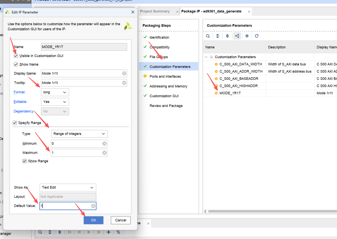
添加1T1R配置属性,并配置为默认1T1R模式
-
参考"创建AD9361接口控制IP核"中的第11到12步内容完成IP核打包。
搭建AD9361回环测试的PL工程
AD9361回环测试的PL工程的框图如下所示:
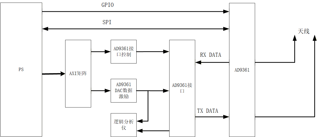
接下来在Vivado工程中搭建AD9361回环测试的PL工程。
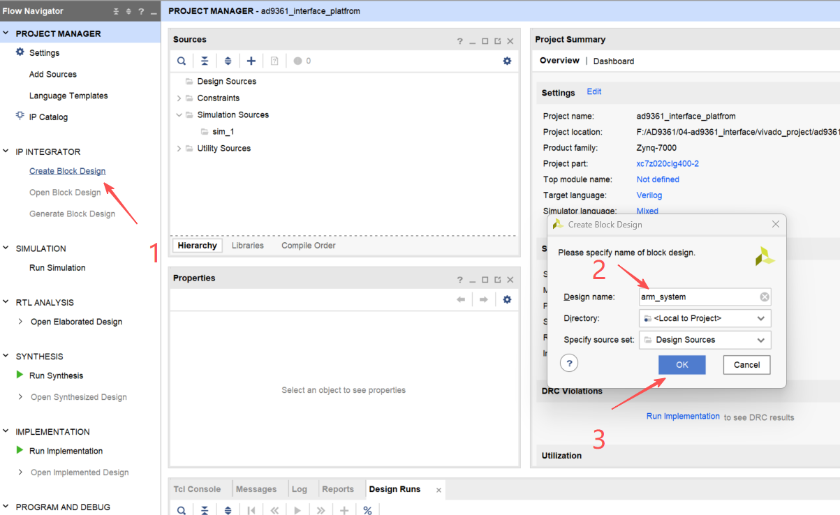
- 创建block design
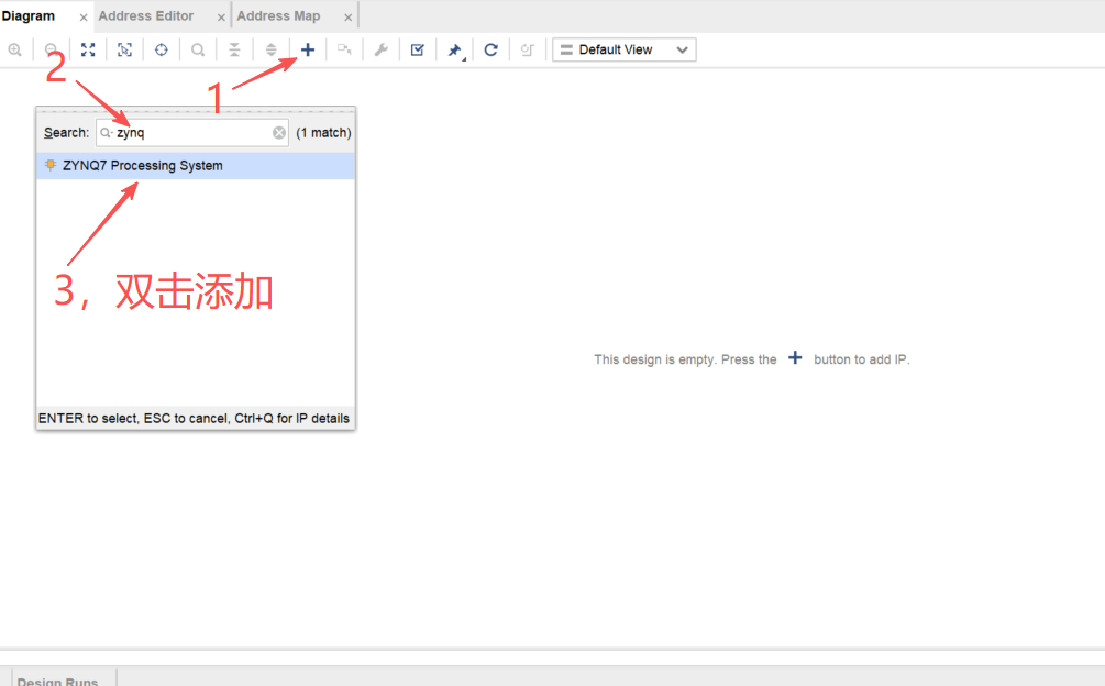
- 添加ZYNQ IP核
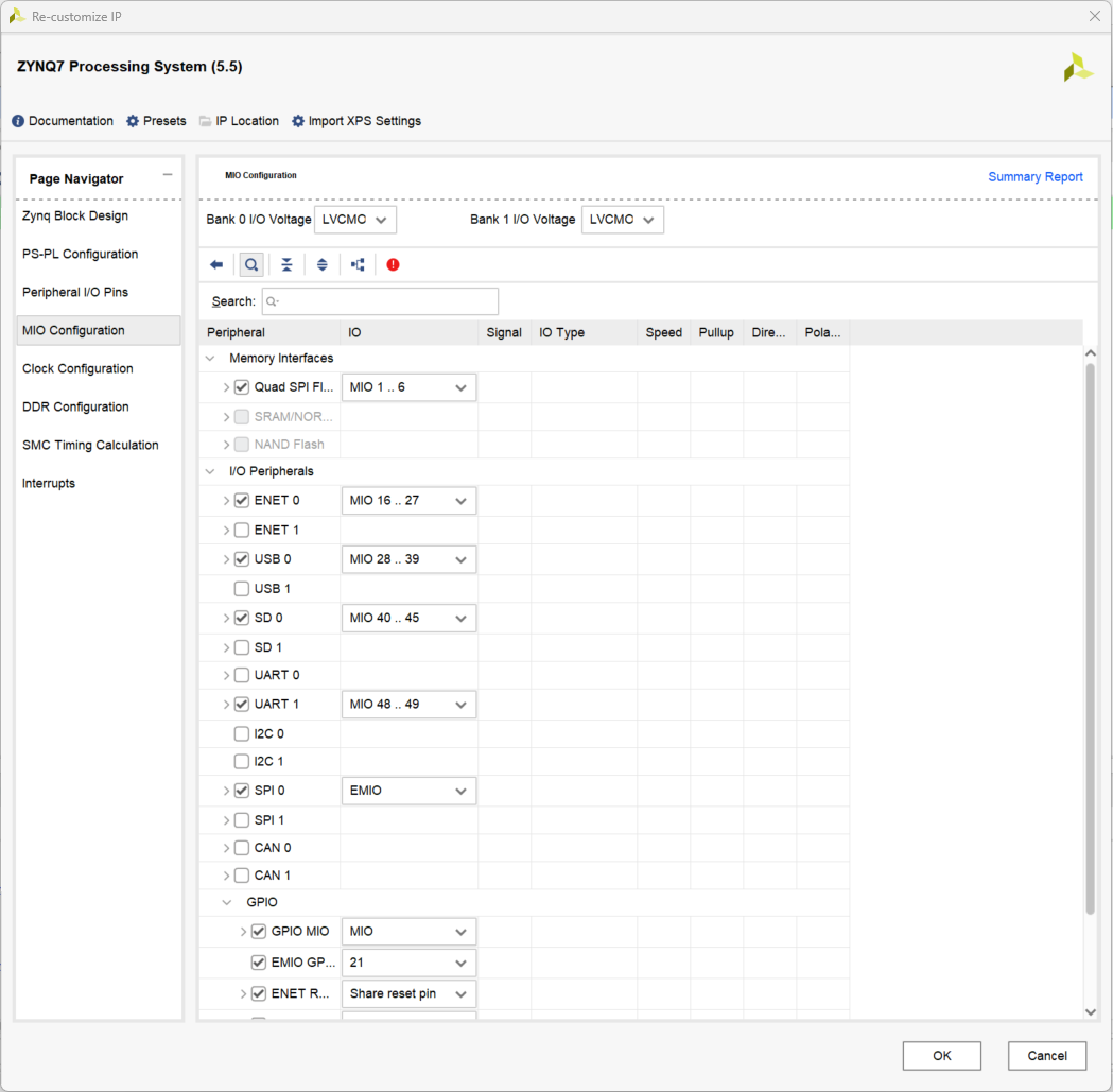
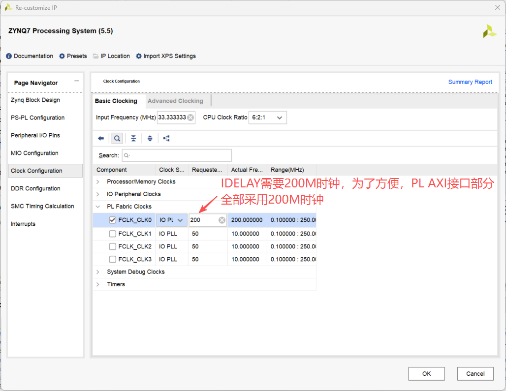
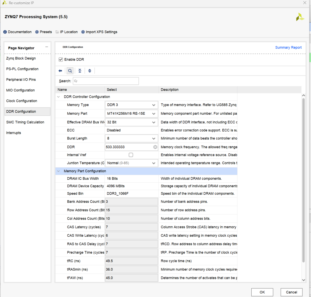
- 配置ZYNQ IP核,其中SPI、EMIO必配,其他的根据板子硬件适当修改,相应的参考配置如下:
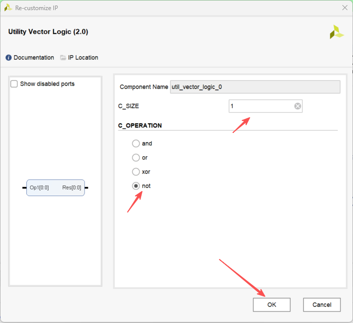
- 参考第2步添加AD9361接口IP核、控制IP核、数据生成IP核、组合逻辑运算IP核,AD9361接口IP核、控制IP核、数据生成IP核默认都是1T1R模式,无需配置。
- 配置组合逻辑IP核为非运算,宽度1位
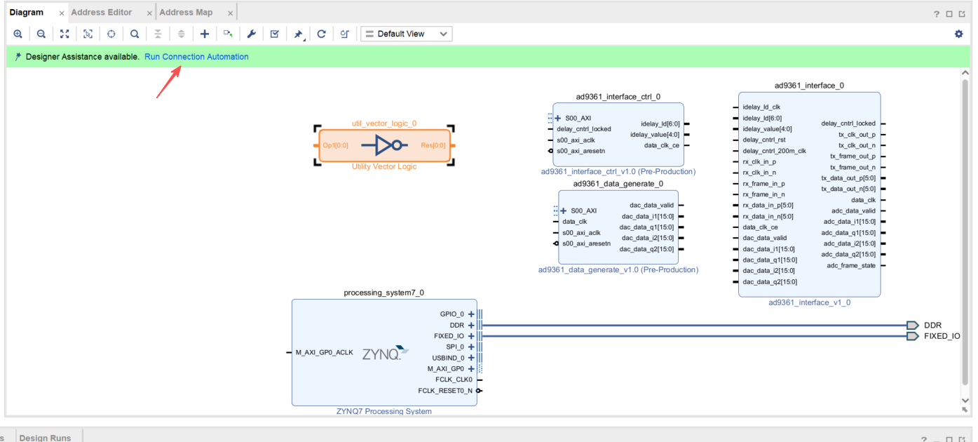
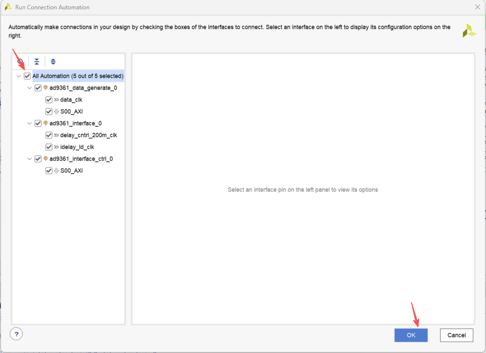
- 点击"Run Connection Automatio",进行一轮自动连线,期间会自动添加AXI矩阵IP核、处理器系统复位IP核
- 连接IDELAY复位信号
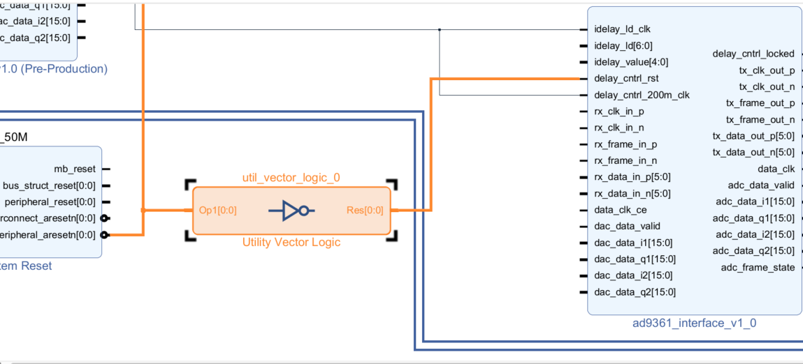
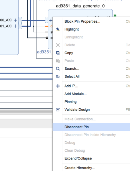
- 重新连接数据生成IP核的数据时钟信号,把以前的连接断开,将其连接到AD9361输出的data_clk上
- 连接IDELAY控制信号
- 给AD9361的ADC数据和DAC数据添加DEBUG
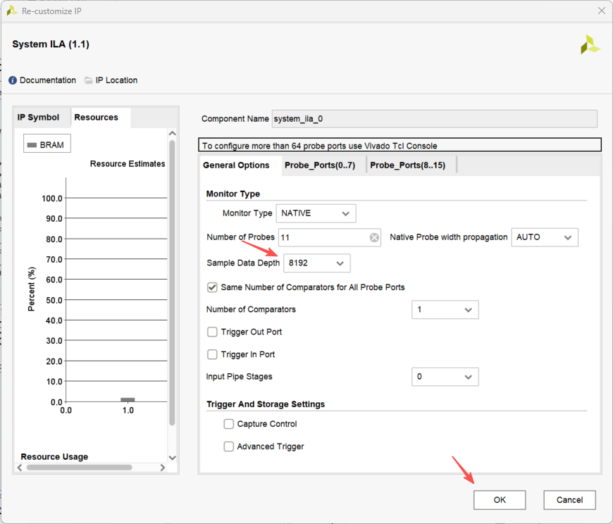
- 将逻辑分析仪采样深度配置为8192,以便能看到更多数据
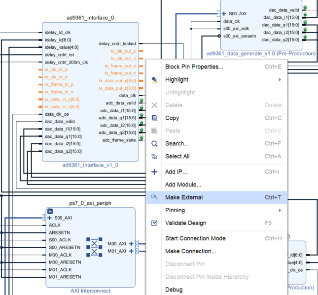
- 将AD9361的引脚引出
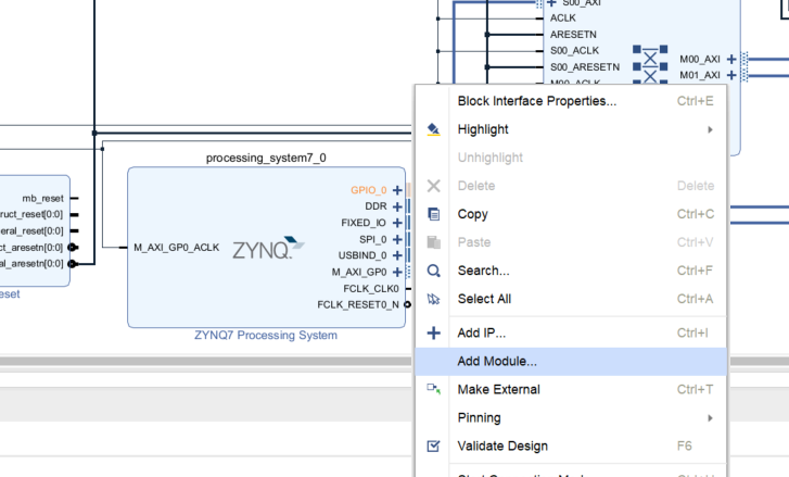
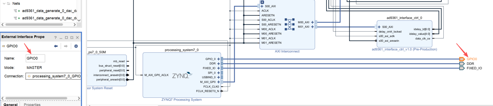
- 将EMIO引脚引出,并改名为GPIO0
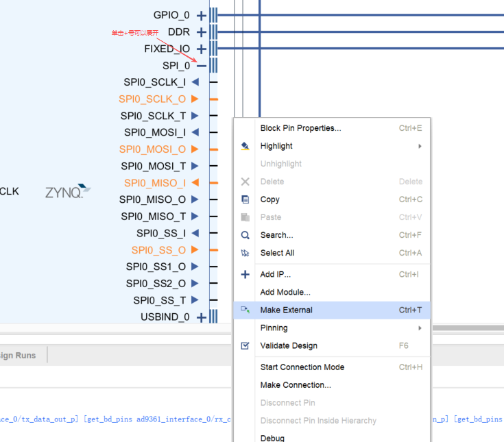
- 将SPI引脚引出,并改名为SPI0_SCLK_O、SPI0_MOSI_O、SPI0_MISO_I、SPI0_SS_O,SPI控制器默认有3个评选,这里只用到1个,所以采样将SPI引脚分别引出的方式。
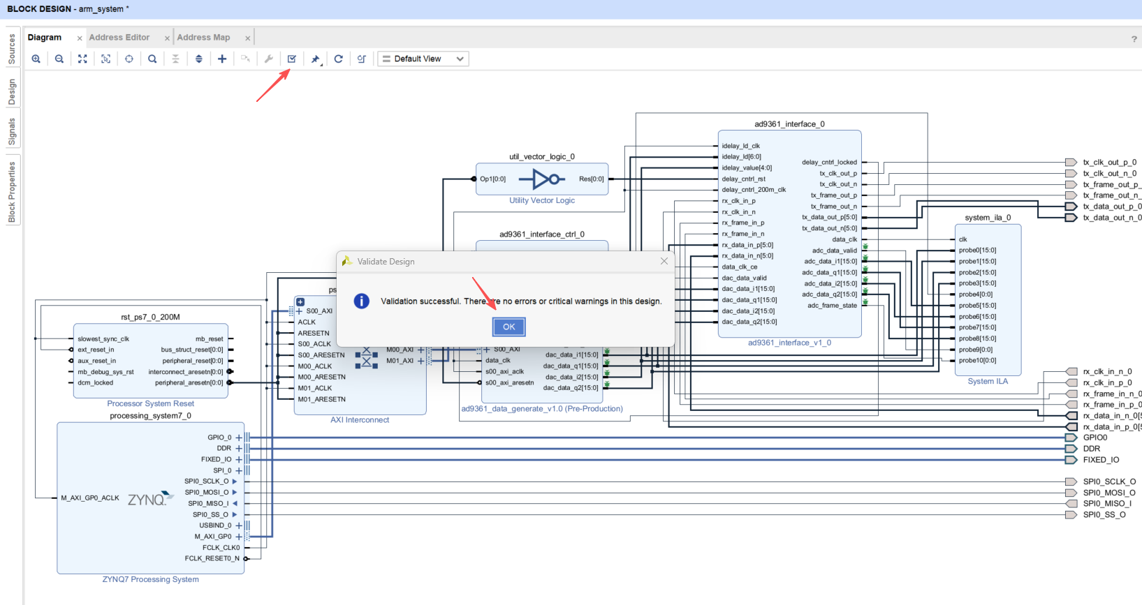
- 验证设计
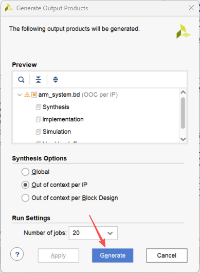
- 生成设计

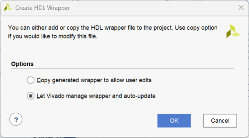
- 创建顶层封装
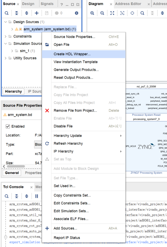
- 添加约束文件
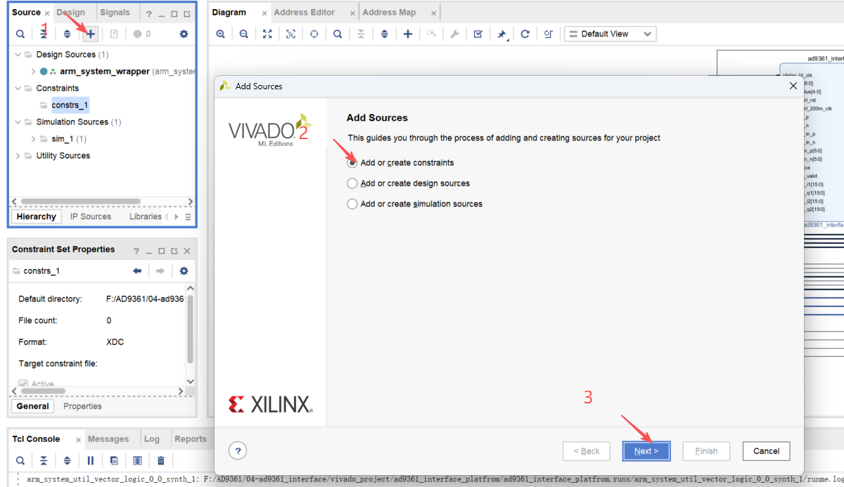
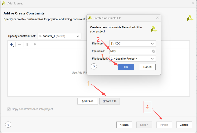
- 编写约束文件,约束文件参考内容如下,具体内容根据原理图进行修改
c
create_clock -name rx_clk_in_p_0 -period 8 [get_ports rx_clk_in_p_0]
set_property -dict {PACKAGE_PIN N20 IOSTANDARD LVDS_25 DIFF_TERM 1} [get_ports rx_clk_in_p_0]
set_property -dict {PACKAGE_PIN P20 IOSTANDARD LVDS_25 DIFF_TERM 1} [get_ports rx_clk_in_n_0]
set_property -dict {PACKAGE_PIN U18 IOSTANDARD LVDS_25 DIFF_TERM 1} [get_ports rx_frame_in_p_0]
set_property -dict {PACKAGE_PIN U19 IOSTANDARD LVDS_25 DIFF_TERM 1} [get_ports rx_frame_in_n_0]
set_property -dict {PACKAGE_PIN Y18 IOSTANDARD LVDS_25 DIFF_TERM 1} [get_ports {rx_data_in_p_0[0]}]
set_property -dict {PACKAGE_PIN Y19 IOSTANDARD LVDS_25 DIFF_TERM 1} [get_ports {rx_data_in_n_0[0]}]
set_property -dict {PACKAGE_PIN V20 IOSTANDARD LVDS_25 DIFF_TERM 1} [get_ports {rx_data_in_p_0[1]}]
set_property -dict {PACKAGE_PIN W20 IOSTANDARD LVDS_25 DIFF_TERM 1} [get_ports {rx_data_in_n_0[1]}]
set_property -dict {PACKAGE_PIN W18 IOSTANDARD LVDS_25 DIFF_TERM 1} [get_ports {rx_data_in_p_0[2]}]
set_property -dict {PACKAGE_PIN W19 IOSTANDARD LVDS_25 DIFF_TERM 1} [get_ports {rx_data_in_n_0[2]}]
set_property -dict {PACKAGE_PIN R16 IOSTANDARD LVDS_25 DIFF_TERM 1} [get_ports {rx_data_in_p_0[3]}]
set_property -dict {PACKAGE_PIN R17 IOSTANDARD LVDS_25 DIFF_TERM 1} [get_ports {rx_data_in_n_0[3]}]
set_property -dict {PACKAGE_PIN V17 IOSTANDARD LVDS_25 DIFF_TERM 1} [get_ports {rx_data_in_p_0[4]}]
set_property -dict {PACKAGE_PIN V18 IOSTANDARD LVDS_25 DIFF_TERM 1} [get_ports {rx_data_in_n_0[4]}]
set_property -dict {PACKAGE_PIN V16 IOSTANDARD LVDS_25 DIFF_TERM 1} [get_ports {rx_data_in_p_0[5]}]
set_property -dict {PACKAGE_PIN W16 IOSTANDARD LVDS_25 DIFF_TERM 1} [get_ports {rx_data_in_n_0[5]}]
set_property -dict {PACKAGE_PIN N18 IOSTANDARD LVDS_25} [get_ports tx_clk_out_p_0]
set_property -dict {PACKAGE_PIN P19 IOSTANDARD LVDS_25} [get_ports tx_clk_out_n_0]
set_property -dict {PACKAGE_PIN T16 IOSTANDARD LVDS_25} [get_ports tx_frame_out_p_0]
set_property -dict {PACKAGE_PIN U17 IOSTANDARD LVDS_25} [get_ports tx_frame_out_n_0]
set_property -dict {PACKAGE_PIN Y16 IOSTANDARD LVDS_25} [get_ports {tx_data_out_p_0[0]}]
set_property -dict {PACKAGE_PIN Y17 IOSTANDARD LVDS_25} [get_ports {tx_data_out_n_0[0]}]
set_property -dict {PACKAGE_PIN U14 IOSTANDARD LVDS_25} [get_ports {tx_data_out_p_0[1]}]
set_property -dict {PACKAGE_PIN U15 IOSTANDARD LVDS_25} [get_ports {tx_data_out_n_0[1]}]
set_property -dict {PACKAGE_PIN V15 IOSTANDARD LVDS_25} [get_ports {tx_data_out_p_0[2]}]
set_property -dict {PACKAGE_PIN W15 IOSTANDARD LVDS_25} [get_ports {tx_data_out_n_0[2]}]
set_property -dict {PACKAGE_PIN W14 IOSTANDARD LVDS_25} [get_ports {tx_data_out_p_0[3]}]
set_property -dict {PACKAGE_PIN Y14 IOSTANDARD LVDS_25} [get_ports {tx_data_out_n_0[3]}]
set_property -dict {PACKAGE_PIN V12 IOSTANDARD LVDS_25} [get_ports {tx_data_out_p_0[4]}]
set_property -dict {PACKAGE_PIN W13 IOSTANDARD LVDS_25} [get_ports {tx_data_out_n_0[4]}]
set_property -dict {PACKAGE_PIN T12 IOSTANDARD LVDS_25} [get_ports {tx_data_out_p_0[5]}]
set_property -dict {PACKAGE_PIN U12 IOSTANDARD LVDS_25} [get_ports {tx_data_out_n_0[5]}]
set_property -dict {PACKAGE_PIN R14 IOSTANDARD LVCMOS25 } [get_ports SPI0_SCLK_O]
set_property -dict {PACKAGE_PIN P15 IOSTANDARD LVCMOS25 } [get_ports SPI0_MOSI_O]
set_property -dict {PACKAGE_PIN R19 IOSTANDARD LVCMOS25 } [get_ports SPI0_MISO_I]
set_property -dict {PACKAGE_PIN P18 IOSTANDARD LVCMOS25 PULLUP true } [get_ports SPI0_SS_O]
set_property -dict {PACKAGE_PIN T11 IOSTANDARD LVCMOS25} [get_ports {GPIO0_tri_io[0]}]
set_property -dict {PACKAGE_PIN T14 IOSTANDARD LVCMOS25} [get_ports {GPIO0_tri_io[1]}]
set_property -dict {PACKAGE_PIN T15 IOSTANDARD LVCMOS25} [get_ports {GPIO0_tri_io[2]}]
set_property -dict {PACKAGE_PIN T17 IOSTANDARD LVCMOS25} [get_ports {GPIO0_tri_io[3]}]
set_property -dict {PACKAGE_PIN T19 IOSTANDARD LVCMOS25} [get_ports {GPIO0_tri_io[4]}]
set_property -dict {PACKAGE_PIN T20 IOSTANDARD LVCMOS25} [get_ports {GPIO0_tri_io[5]}]
set_property -dict {PACKAGE_PIN U13 IOSTANDARD LVCMOS25} [get_ports {GPIO0_tri_io[6]}]
set_property -dict {PACKAGE_PIN V13 IOSTANDARD LVCMOS25} [get_ports {GPIO0_tri_io[7]}]
set_property -dict {PACKAGE_PIN T10 IOSTANDARD LVCMOS25} [get_ports {GPIO0_tri_io[8]}]
set_property -dict {PACKAGE_PIN J14 IOSTANDARD LVCMOS33} [get_ports {GPIO0_tri_io[9]}]
set_property -dict {PACKAGE_PIN N15 IOSTANDARD LVCMOS33} [get_ports {GPIO0_tri_io[10]}]
set_property -dict {PACKAGE_PIN N16 IOSTANDARD LVCMOS33} [get_ports {GPIO0_tri_io[11]}]
set_property -dict {PACKAGE_PIN P14 IOSTANDARD LVCMOS25} [get_ports {GPIO0_tri_io[12]}]
set_property -dict {PACKAGE_PIN R18 IOSTANDARD LVCMOS25} [get_ports {GPIO0_tri_io[13]}]
set_property -dict {PACKAGE_PIN P16 IOSTANDARD LVCMOS25} [get_ports {GPIO0_tri_io[14]}]
set_property -dict {PACKAGE_PIN U20 IOSTANDARD LVCMOS25} [get_ports {GPIO0_tri_io[15]}]
set_property -dict {PACKAGE_PIN N17 IOSTANDARD LVCMOS25} [get_ports {GPIO0_tri_io[16]}]
set_property -dict {PACKAGE_PIN C20 IOSTANDARD LVCMOS33} [get_ports {GPIO0_tri_io[17]}]
set_property -dict {PACKAGE_PIN B20 IOSTANDARD LVCMOS33} [get_ports {GPIO0_tri_io[18]}]
set_property -dict {PACKAGE_PIN B19 IOSTANDARD LVCMOS33} [get_ports {GPIO0_tri_io[19]}]
set_property -dict {PACKAGE_PIN A20 IOSTANDARD LVCMOS33} [get_ports {GPIO0_tri_io[20]}]
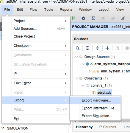
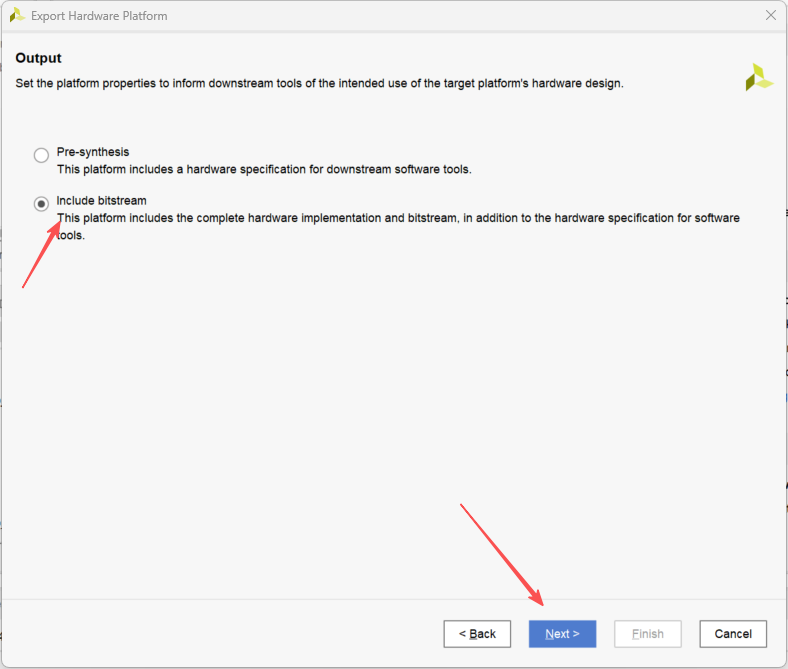
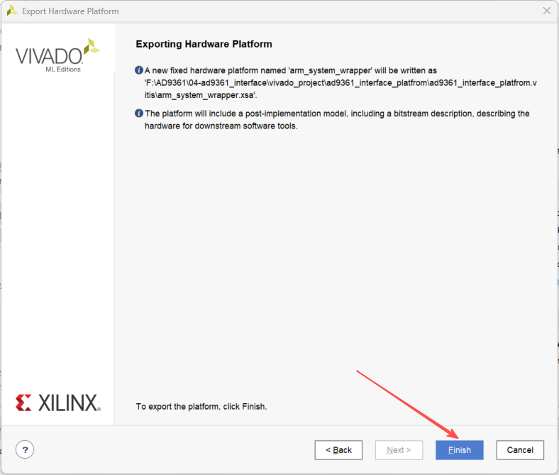
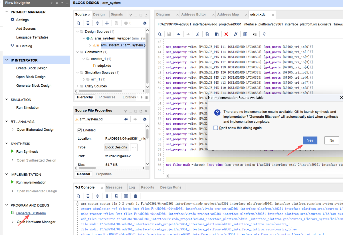
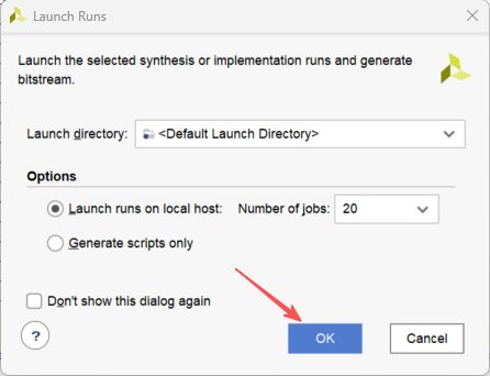
set_false_path -through [get_pins {arm_system_i/ad9361_interface_ctrl_0/inst/ad9361_interface_ctrl_v1_0_S00_AXI_inst/data_clk_ce_reg/C}]- 生成BIT流
- 导出处硬件描述文件,导出成功后会在相应目录下生成一个.xsa的文件。