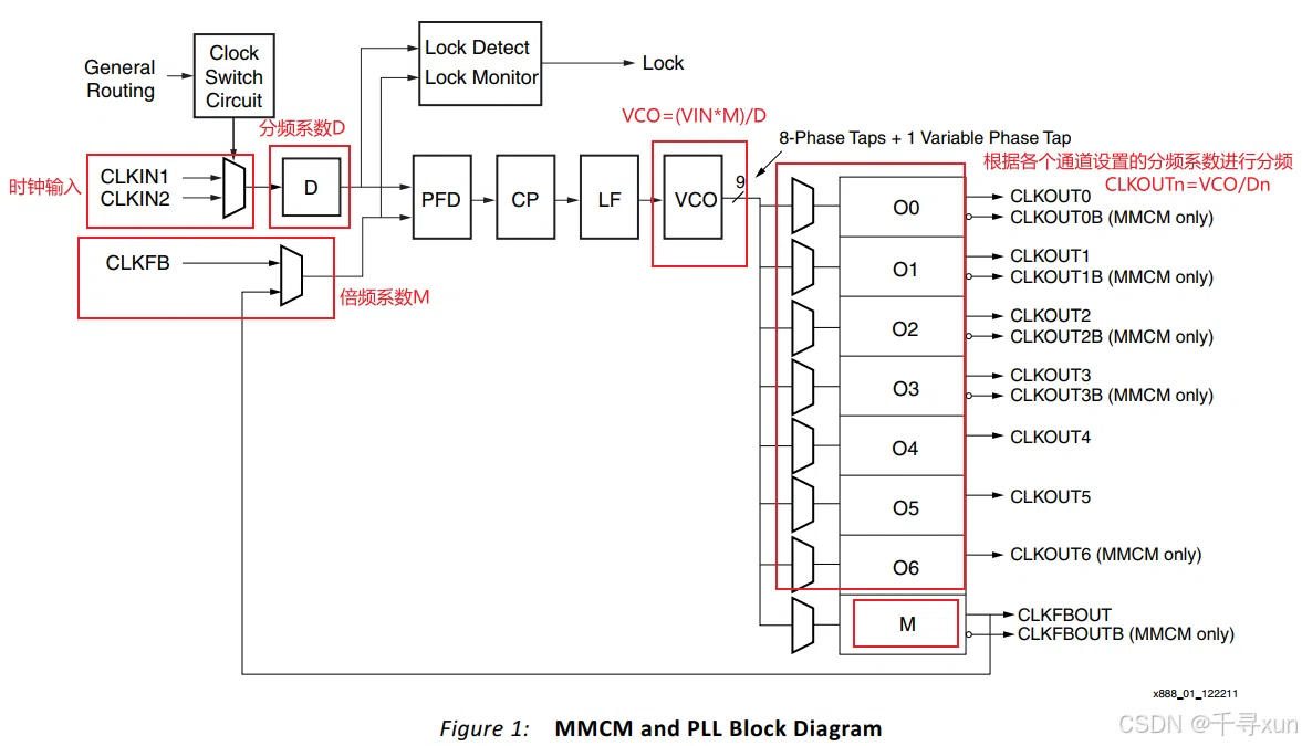
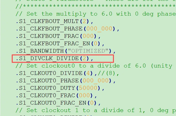
老师,您好,可以给我讲讲xilinx mmcm 这个框图嘛,原理,我作为一名fpga工程师如何使用drp功能;文件如上,然后有一个问题, top_mmcme2.v文件中.S1_DIVCLK_DIVIDE(2),是啥意思,谢谢您
你好!很高兴为你解答。作为FPGA工程师,理解MMCM(Mixed-Mode Clock Manager)和DRP(Dynamic Reconfiguration Port)是进阶的必备技能。我们分三部分来回答:框图原理 、代码中的参数含义 、以及如何使用DRP功能。
一、 Xilinx MMCM 框图原理详解
你提供的图片是Xilinx 7系列FPGA中MMCM的经典结构图。我们可以把它看作一个**"频率合成工厂"**,流程如下:
-
输入与预分频(D):
-
左侧
CLKIN1/2是外部晶振或时钟输入。 -
进入
D触发器(实际上是分频器),对应参数DIVCLK_DIVIDE。 -
作用:如果输入时钟频率太高,先除以D,降低频率,以便后续电路处理。
-
公式:FPFD=FCLKIN/DFPFD=FCLKIN/D
-
-
鉴频鉴相器(PFD)与电荷泵(CP)、环路滤波器(LF):
-
PFD 比较
CLKFB(反馈时钟)和经过D分频后的时钟的相位差。 -
输出误差信号,控制VCO(压控振荡器)的频率。
-
-
压控振荡器(VCO)与倍频(M):
-
这是核心。VCO输出高频时钟。
-
反馈路径上的
M(CLKFBOUT_MULT_F)是倍频系数。 -
核心公式:FVCO=FCLKIN×MDFVCO=FCLKIN×DM
-
注意:VCO的频率必须在芯片规定的范围内(例如 600MHz - 1200MHz),否则MMCM无法锁定(Lock)。
-
-
输出分频(O0 - O6):
-
VCO产生的高频信号,经过右侧的
O0到O6分频器输出。 -
每个输出通道都可以独立设置分频系数(
CLKOUTx_DIVIDE)和相位(Phase)。 -
输出公式:FOUTx=FVCOOxFOUTx=OxFVCO
-
总结:MMCM就像一个齿轮箱,输入频率先被D除,再被M乘,最后被O除,得到你想要的频率。
二、 关于 .S1_DIVCLK_DIVIDE(2) 的问题
在 top_mmcme2.v 文件中,这行代码的含义是:
这是配置"状态1(State 1)"下的输入时钟分频系数(D)= 2。
具体解释:
-
S1:代表 State 1。你的代码支持动态重配置(DRP),可以在不同状态间切换。这里定义的是第一种配置方案。
-
DIVCLK_DIVIDE :对应框图中最左边的
D。 -
值为 2:意味着输入的时钟频率会被除以 2。
结合你的代码看:
-
输入时钟
CLKIN_PERIOD设为 10.000 ns,即 100 MHz。 -
在
mmcme2_drp模块中,S1_CLKFBOUT_MULT设为 2(倍频 M=2)。 -
那么 VCO 的频率计算为:FVCO=100MHz×22=100MHzFVCO=100MHz×22=100MHz。
-
如果
S1_DIVCLK_DIVIDE(2)改成 1,那么 FVCO=100MHz×21=200MHzFVCO=100MHz×12=200MHz。
为什么设为2?
通常是为了满足VCO的工作频率范围,或者为了得到特定的输出频率。如果你的输入时钟很高(比如 500MHz),D必须设大一点,否则VCO会超频。
三、 FPGA工程师如何使用 DRP 功能
DRP(Dynamic Reconfiguration Port)允许你在FPGA运行过程中,动态修改MMCM的配置参数(如倍频M、分频D、输出分频O、相位等),而不需要重新烧录比特流。
1. 核心文件解析
你提供的代码包含三个关键部分:
-
mmcme2_drp.v:DRP状态机。它负责读取ROM中的配置数据,并通过DRP接口写入MMCM。 -
mmcme2_drp_func.h:计算函数。它把用户设置的参数(如M=2, D=2)转换成MMCM寄存器能识别的二进制值(Bitmask)。 -
top_mmcme2.v:顶层模块。它实例化了MMCME2_ADV(硬核)和mmcme2_drp(控制器),并连接了DRP信号。
2. 使用步骤(基于你的代码)
你的代码设计了一个多状态重配置的机制。
-
Step 1: 定义状态参数
在
mmcme2_drp实例化时,你会看到S1_,S2_,S3_开头的参数。-
S1_...:第一种配置(例如:100MHz输入,输出50MHz)。 -
S2_...:第二种配置(例如:100MHz输入,输出200MHz)。 -
S3_...:第三种配置。
-
-
Step 2: 触发重配置
在
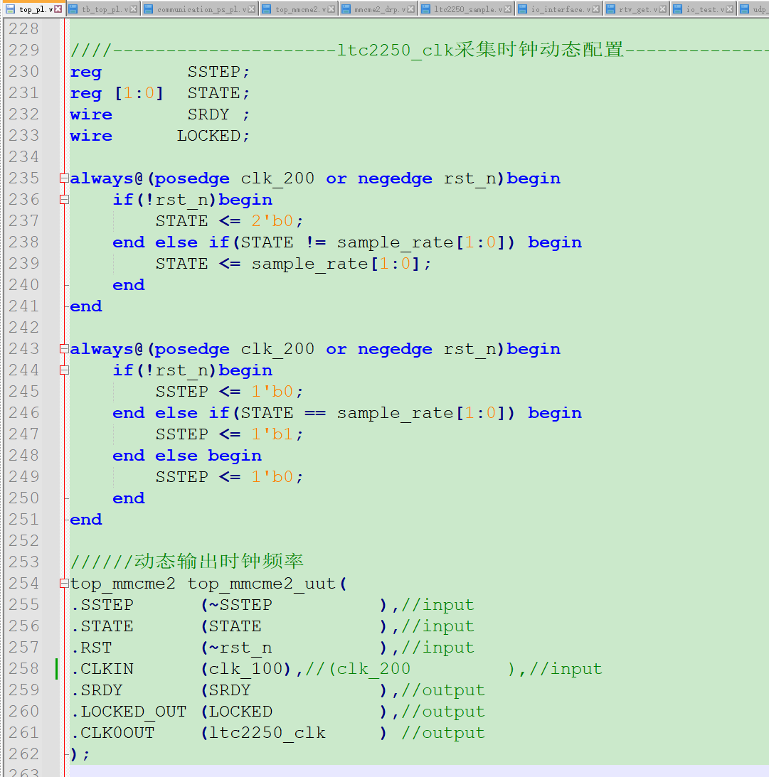
top_mmcme2.v的端口有input SSTEP和input [1:0] STATE。-
STATE:选择你要切换到哪一组参数(0对应S1,1对应S2,2对应S3)。
-
SSTEP:给一个脉冲(上升沿),启动重配置过程。
-
-
Step 3: 内部工作流程
-
你改变
STATE引脚的值。 -
给
SSTEP一个脉冲。 -
mmcme2_drp模块检测到SSTEP,开始工作。 -
它根据
STATE选择对应的 ROM 地址段(比如 S2 的地址)。 -
它通过
DADDR,DI,DEN,DWE信号,将新配置写入MMCME2_ADV。 -
写入完成后,MMCM会暂时失锁(LOST LOCK),然后重新锁定(LOCKED)。
-
SRDY信号拉高,表示重配置完成。
-
3. 注意事项(避坑指南)
-
时钟切换风险 :在重配置过程中,输出时钟会不稳定甚至停止。如果你的系统依赖这个时钟运行逻辑,必须 设计好时钟切换电路(BUFGMUX),在DRP操作期间切换到备用时钟(如晶振直连),等待
LOCKED信号再次变高后,再切回来。 -
VCO频率范围:无论你怎么重配置,计算出的 FVCOFVCO 必须满足芯片手册要求(7系列通常是 600MHz - 1200MHz)。否则MMCM无法锁定。
-
复位 :重配置期间,
RST_MMCM信号会被拉高,这是正常的,为了重置MMCM内部状态。
总结 :你图中的红框 .S1_DIVCLK_DIVIDE(2) 只是定义了第一套配置方案中的输入分频系数。要使用DRP,你只需要在外部改变 STATE 并触发 SSTEP,剩下的寄存器计算和写入由 mmcme2_drp.v 自动完成。
top_mmcme2.v
//------------------------------------------------------------------------------------------
//   ____  ____
//  /   /\/   /
// /___/  \  /
// \   \   \/    锟? Copyright 2019 Xilinx, Inc. All rights reserved.
//  \   \        This file contains confidential and proprietary information of Xilinx, Inc.
//  /   /        and is protected under U.S. and international copyright and other
// /___/   /\    intellectual property laws.
// \   \  /  \
//  \___\/\___\
//
//-------------------------------------------------------------------------------------------
// Device:              7-Series
// Author:              Tatsukawa, Kruger, Defossez
// Entity Name:         top_mmcme2
// Purpose:             This is a basic demonstration of the MMCM_DRP
//                      connectivity to the MMCM_ADV.
// Tools:               Vivado_2019.1 or newer
// Limitations:
//
// Vendor:              Xilinx Inc.
// Version:             1.40
// Filename:            top_mmcme2.v
// Date Created:        30-Jul-2014
// Date Last Modified:  25-Jun-2019
//-------------------------------------------------------------------------------------------
// Disclaimer:
//		This disclaimer is not a license and does not grant any rights to the materials
//		distributed herewith. Except as otherwise provided in a valid license issued to you
//		by Xilinx, and to the maximum extent permitted by applicable law: (1) THESE MATERIALS
//		ARE MADE AVAILABLE "AS IS" AND WITH ALL FAULTS, AND XILINX HEREBY DISCLAIMS ALL
//		WARRANTIES AND CONDITIONS, EXPRESS, IMPLIED, OR STATUTORY, INCLUDING BUT NOT LIMITED
//		TO WARRANTIES OF MERCHANTABILITY, NON-INFRINGEMENT, OR FITNESS FOR ANY PARTICULAR
//		PURPOSE; and (2) Xilinx shall not be liable (whether in contract or tort, including
//		negligence, or under any other theory of liability) for any loss or damage of any
//		kind or nature related to, arising under or in connection with these materials,
//		including for any direct, or any indirect, special, incidental, or consequential
//		loss or damage (including loss of data, profits, goodwill, or any type of loss or
//		damage suffered as a result of any action brought by a third party) even if such
//		damage or loss was reasonably foreseeable or Xilinx had been advised of the
//		possibility of the same.
//
// CRITICAL APPLICATIONS
//		Xilinx products are not designed or intended to be fail-safe, or for use in any
//		application requiring fail-safe performance, such as life-support or safety devices
//		or systems, Class III medical devices, nuclear facilities, applications related to
//		the deployment of airbags, or any other applications that could lead to death,
//		personal injury, or severe property or environmental damage (individually and
//		collectively, "Critical Applications"). Customer assumes the sole risk and
//		liability of any use of Xilinx products in Critical Applications, subject only to
//		applicable laws and regulations governing limitations on product liability.
//
// THIS COPYRIGHT NOTICE AND DISCLAIMER MUST BE RETAINED AS PART OF THIS FILE AT ALL TIMES.
//
// Contact:    e-mail  hotline@xilinx.com        phone   + 1 800 255 7778
//-------------------------------------------------------------------------------------------
// Revision History:
//  Rev: 30-Apr-2014 - Tatsukawa
//      Initial code release
//  Rev: 25-Jun-2019 - Defossez
//      Add possibility to register the LOCKED signal.
//-------------------------------------------------------------------------------------------
//
`timescale 1ps/1ps
//
//-------------------------------------------------------------------------------------------
// Entity pin description
//-------------------------------------------------------------------------------------------
// Inputs
//      SSTEP:      Start a reconfiguration. It should only be pulsed for one clock cycle.
//      STATE:      Determines which state the MMCM_ADV will be reconfigured to. A value
//                  of 0 correlates to state 1, and a value of 1 correlates to state 2.
//      RST:        RST will reset the entire reference design including the MMCM_ADV.
//      CLKIN:      Clock for the MMCM_ADV CLKIN as well as the clock for the MMCM_DRP module
//      SRDY:       Pulses for one clock cycle after the MMCM_ADV is locked and the
//                  MMCM_DRP module is ready to start another re-configuration.
// Outputs
//      LOCKED_OUT: MMCM is locked after configuration or reconfiguration.
//      CLK0OUT:    These are the clock outputs from the MMCM_ADV.
//      CLK1OUT:    These are the clock outputs from the MMCM_ADV.
//      CLK2OUT:    These are the clock outputs from the MMCM_ADV.
//      CLK3OUT:    These are the clock outputs from the MMCM_ADV.
//      CLK4OUT:    These are the clock outputs from the MMCM_ADV.
//      CLK5OUT:    These are the clock outputs from the MMCM_ADV.
//      CLK6OUT:    These are the clock outputs from the MMCM_ADV.
//-------------------------------------------------------------------------------------------
module top_mmcme2
    (
        input    SSTEP,
        input [1:0]   STATE,
        input    RST,
        input    CLKIN,
        output   SRDY,
 		output 	 LOCKED_OUT,
        output   CLK0OUT,
        output   CLK1OUT,
        output   CLK2OUT,
        output   CLK3OUT,
        output   CLK4OUT,
        output   CLK5OUT,
        output   CLK6OUT
    );
//-------------------------------------------------------------------------------------------
// These signals are used as direct connections between the MMCM_ADV and the
// MMCM_DRP.
(* mark_debug = "true" *) wire [15:0]    di;
(* mark_debug = "true" *) wire [6:0]     daddr;
(* mark_debug = "true" *) wire [15:0]    dout;
(* mark_debug = "true" *) wire           den;
(* mark_debug = "true" *) wire           dwe;
wire            dclk;
wire            rst_mmcm;
wire            drdy;
reg				current_state;
reg [7:0]		sstep_int ;
reg				init_drp_state = 1;
// These signals are used for the BUFG's necessary for the design.
wire            CLKIN_ibuf;
wire            clkin_bufgout;
wire            clkfb_bufgout;
wire            clkfb_bufgin;
wire            clk0_bufgin;
wire            clk0_bufgout;
wire            clk1_bufgin;
wire            clk1_bufgout;
wire            clk2_bufgin;
wire            clk2_bufgout;
wire            clk3_bufgin;
wire            clk3_bufgout;
wire            clk4_bufgin;
wire            clk4_bufgout;
wire            clk5_bufgin;
wire            clk5_bufgout;
wire            clk6_bufgin;
wire            clk6_bufgout;
wire            LOCKED;
//-------------------------------------------------------------------------------------------
assign CLKIN_ibuf = CLKIN;
//
BUFG BUFG_IN    (.O (clkin_bufgout),    .I (CLKIN_ibuf));
BUFG BUFG_FB    (.O (clkfb_bufgout),    .I (clkfb_bufgin));
BUFG BUFG_CLK0  (.O (CLK0OUT),     .I (clk0_bufgin));
BUFG BUFG_CLK1  (.O (clk1_bufgout),     .I (clk1_bufgin));
BUFG BUFG_CLK2  (.O (clk2_bufgout),     .I (clk2_bufgin));
BUFG BUFG_CLK3  (.O (clk3_bufgout),     .I (clk3_bufgin));
BUFG BUFG_CLK4  (.O (clk4_bufgout),     .I (clk4_bufgin));
BUFG BUFG_CLK5  (.O (clk5_bufgout),     .I (clk5_bufgin));
BUFG BUFG_CLK6  (.O (clk6_bufgout),     .I (clk6_bufgin));
//
// ODDR registers used to output clocks
// ODDR ODDR_CLK0 (.Q(CLK0OUT), .C(clk0_bufgout), .CE(1'b1), .D1(1'b1), .D2(1'b0), .R(RST), .S(1'b0));
ODDR ODDR_CLK1 (.Q(CLK1OUT), .C(clk1_bufgout), .CE(1'b1), .D1(1'b1), .D2(1'b0), .R(RST), .S(1'b0));
ODDR ODDR_CLK2 (.Q(CLK2OUT), .C(clk2_bufgout), .CE(1'b1), .D1(1'b1), .D2(1'b0), .R(RST), .S(1'b0));
ODDR ODDR_CLK3 (.Q(CLK3OUT), .C(clk3_bufgout), .CE(1'b1), .D1(1'b1), .D2(1'b0), .R(RST), .S(1'b0));
ODDR ODDR_CLK4 (.Q(CLK4OUT), .C(clk4_bufgout), .CE(1'b1), .D1(1'b1), .D2(1'b0), .R(RST), .S(1'b0));
ODDR ODDR_CLK5 (.Q(CLK5OUT), .C(clk5_bufgout), .CE(1'b1), .D1(1'b1), .D2(1'b0), .R(RST), .S(1'b0));
ODDR ODDR_CLK6 (.Q(CLK6OUT), .C(clk6_bufgout), .CE(1'b1), .D1(1'b1), .D2(1'b0), .R(RST), .S(1'b0));
//
// MMCM_ADV that reconfiguration will take place on
//
//  BANDWIDTH:              : "HIGH", "LOW" or "OPTIMIZED"
//  DIVCLK_DIVIDE           : Value from 1 to 106
//  CLKFBOUT_MULT_F         : Value from 2 to 64
//  CLKFBOUT_PHASE          :
//  CLKFBOUT_USE_FINE_PS    : "TRUE" or "FALSE",
//  CLKIN1_PERIOD           : Value from 0.968 to 100.000. Set the period (ns) of input clocks
//  REF_JITTER1             :
//  CLKIN2_PERIOD           :
//  REF_JITTER2             :
//  CLKOUT parameters:
//  DIVIDE                  : Value from 1 to 128
//  DUTY_CYCLE              : 0.01 to 0.99 - This is dependent on the divide value.
//  PHASE                   : 0.0 to 360.0 - This is dependent on the divide value.
//  USE_FINE_PS             : TRUE or FALSE
//  Misc parameters
//  COMPENSATION
//  STARTUP_WAIT
//  -------------------Fclkin 输入时钟频率
//  -------------------Fvco = (Fclkin * M) /D  ---- Fvco电压控制振荡器内部频率
//  -------------------Fout(x) = Fvco/O(x)     ---- O(x)--CLKOUTx 的分频系数
MMCME2_ADV #(
   .BANDWIDTH           ("OPTIMIZED"),
   .DIVCLK_DIVIDE       (1),  //D分频参数  输入时钟分频器(DIVCLK_DIVIDE)
   .CLKFBOUT_MULT_F     (6),//(3),  //M倍频参数  倍频因子(CLKFBOUT_MULT_F)
   .CLKFBOUT_PHASE      (0.0),
   .CLKFBOUT_USE_FINE_PS("FALSE"),
   .CLKIN1_PERIOD       (10.000),//(5.000),
   .REF_JITTER1         (0.010),
   .CLKIN2_PERIOD       (10.000),
   .REF_JITTER2         (0.010),
   .CLKOUT0_DIVIDE_F    (24),//(24),//CLKOUTx 的分频系数
   .CLKOUT0_DUTY_CYCLE  (0.5),
   .CLKOUT0_PHASE       (0.0),
   .CLKOUT0_USE_FINE_PS ("FALSE"),
   .CLKOUT1_DIVIDE      (6), //
   .CLKOUT1_DUTY_CYCLE  (0.5),
   .CLKOUT1_PHASE       (0.0),
   .CLKOUT1_USE_FINE_PS ("FALSE"),
   .CLKOUT2_DIVIDE      (6),
   .CLKOUT2_DUTY_CYCLE  (0.5),
   .CLKOUT2_PHASE       (0.0),
   .CLKOUT2_USE_FINE_PS ("FALSE"),
   .CLKOUT3_DIVIDE      (6),
   .CLKOUT3_DUTY_CYCLE  (0.5),
   .CLKOUT3_PHASE       (0.0),
   .CLKOUT3_USE_FINE_PS ("FALSE"),
   .CLKOUT4_DIVIDE      (6),
   .CLKOUT4_DUTY_CYCLE  (0.5),
   .CLKOUT4_PHASE       (0.0),
   .CLKOUT4_USE_FINE_PS ("FALSE"),
   .CLKOUT4_CASCADE     ("FALSE"),
   .CLKOUT5_DIVIDE      (6),
   .CLKOUT5_DUTY_CYCLE  (0.5),
   .CLKOUT5_PHASE       (0.0),
   .CLKOUT5_USE_FINE_PS ("FALSE"),
   .CLKOUT6_DIVIDE      (6),
   .CLKOUT6_DUTY_CYCLE  (0.5),
   .CLKOUT6_PHASE       (0.0),
   .CLKOUT6_USE_FINE_PS ("FALSE"),
   .COMPENSATION        ("ZHOLD"),
   .STARTUP_WAIT        ("FALSE")
) mmcme2_test_inst (
   .CLKFBOUT            (clkfb_bufgin),
   .CLKFBOUTB           (),
   .CLKFBSTOPPED        (),
   .CLKINSTOPPED        (),
   .CLKOUT0             (clk0_bufgin),
   .CLKOUT0B            (),
   .CLKOUT1             (clk1_bufgin),
   .CLKOUT1B            (),
   .CLKOUT2             (clk2_bufgin),
   .CLKOUT2B            (),
   .CLKOUT3             (clk3_bufgin),
   .CLKOUT3B            (),
   .CLKOUT4             (clk4_bufgin),
   .CLKOUT5             (clk5_bufgin),
   .CLKOUT6             (clk6_bufgin),
   .DO                  (dout),
   .DRDY                (drdy),
   .DADDR               (daddr),
   .DCLK                (dclk),
   .DEN                 (den),
   .DI                  (di),
   .DWE                 (dwe),
   .LOCKED              (LOCKED),
   .CLKFBIN             (clkfb_bufgout),
   .CLKIN1              (clkin_bufgout),
   .CLKIN2              (),
   .CLKINSEL            (1'b1),
   .PSDONE              (),
   .PSCLK               (1'b0),
   .PSEN                (1'b0),
   .PSINCDEC            (1'b0),
   .PWRDWN              (1'b0),
   .RST                 (rst_mmcm)
);
// MMCM_DRP instance that will perform the reconfiguration operations
mmcme2_drp #(
    // Register the LOCKED signal with teh MMCME3_ADV input clock.
    // The LOCKED_IN (LOCKED from the MMCME3_ADV) is fed into a register and then
    // passed the LOCKED_OUT when REGISTER_LOCKED is set to "Reg" or when set to
    // "NoReg" LOCKED_IN is just passed on to LOCKED_OUT without being registered.
    .REGISTER_LOCKED       ("Reg"),
    // Use the registered LOCKED signal from the MMCME3 also for the DRP state machine.
    .USE_REG_LOCKED        ("No"),
    // Possible combination of above two parameters:
    // | REGISTER_LOCKED | USE_REG_LOCKED |                                            |
    // |-----------------|----------------|--------------------------------------------|
    // |      "NoReg"    |     "No"       | LOCKED is just passed through mmcme3_drp   |
    // |                 |                | and is used as is with the state machine   |
    // |      "NoReg"    |     "Yes"      | NOT ALLOWED                                |
    // |       "Reg"     |     "No"       | LOCKED is registered but the unregistered  |
    // |                 |                | version is used for the state machine.     |
    // |       "Reg"     |     "Yes"      | LOCKED is registered and the registered    |
    // |                 |                | version is also used by the state machine. |
    //
    //***********************************************************************
    // State 1 Parameters - These are for the first reconfiguration state.
    //***********************************************************************
    // Set the multiply to 6.0 with 0 deg phase offset, optimized bandwidth, input divide of 1
    .S1_CLKFBOUT_MULT(2),
    .S1_CLKFBOUT_PHASE(000_000),
    .S1_CLKFBOUT_FRAC(000),
    .S1_CLKFBOUT_FRAC_EN(0),
    .S1_BANDWIDTH("OPTIMIZED"),
    .S1_DIVCLK_DIVIDE(2),
    // Set clockout0 to a divide of 6.0 (unity gain), 0 deg phase offset, 50/50 duty cycle
    .S1_CLKOUT0_DIVIDE(4),//(8),
    .S1_CLKOUT0_PHASE(000_000),
    .S1_CLKOUT0_DUTY(50000),
    .S1_CLKOUT0_FRAC(000),
    .S1_CLKOUT0_FRAC_EN(0),
    // Set clockout 1 to a divide of 1, 0 deg phase offset, 50/50 duty cycle
    .S1_CLKOUT1_DIVIDE(1),
    .S1_CLKOUT1_PHASE(000_000),
    .S1_CLKOUT1_DUTY(50000),
    // Set clockout 2 to a divide of 2, 0 deg phase offset, 50/50 duty cycle
    .S1_CLKOUT2_DIVIDE(2),
    .S1_CLKOUT2_PHASE(000_000),
    .S1_CLKOUT2_DUTY(50000),
    // Set clockout 3 to a divide of 3, 0 deg phase offset, 50/50 duty cycle
    .S1_CLKOUT3_DIVIDE(3),
    .S1_CLKOUT3_PHASE(000_000),
    .S1_CLKOUT3_DUTY(50000),
    // Set clockout 4 to a divide of 4, 0 deg phase offset, 50/50 duty cycle
    .S1_CLKOUT4_DIVIDE(4),
    .S1_CLKOUT4_PHASE(000_000),
    .S1_CLKOUT4_DUTY(50000),
    // Set clockout 5 to a divide of 5, 0 deg phase offset, 50/50 duty cycle
    .S1_CLKOUT5_DIVIDE(5),
    .S1_CLKOUT5_PHASE(000_000),
    .S1_CLKOUT5_DUTY(50000),
    // Set clockout 6 to a divide of 10, 0 deg phase offset, 50/50 duty cycle
    .S1_CLKOUT6_DIVIDE(10),
    .S1_CLKOUT6_PHASE(000_000),
    .S1_CLKOUT6_DUTY(50000),
    //***********************************************************************
    // State 2 Parameters - These are for the second reconfiguration state.
    //***********************************************************************
    .S2_CLKFBOUT_MULT(2),
    .S2_CLKFBOUT_PHASE(000_000),
    .S2_CLKFBOUT_FRAC(000),
    .S2_CLKFBOUT_FRAC_EN(0),
    .S2_BANDWIDTH("OPTIMIZED"),
    .S2_DIVCLK_DIVIDE(2),
    // Set clockout 0 to a divide of 4.750, 0 deg phase offset, 50/50 duty cycle
    .S2_CLKOUT0_DIVIDE(2),//(4),
    .S2_CLKOUT0_PHASE(000_000),
    .S2_CLKOUT0_DUTY(50000),
    .S2_CLKOUT0_FRAC(000),
    .S2_CLKOUT0_FRAC_EN(0),
    // Set clockout 1 to a divide of 1, 45.0 deg phase offset, 50/50 duty cycle
    .S2_CLKOUT1_DIVIDE(1),
    .S2_CLKOUT1_PHASE(045_000),
    .S2_CLKOUT1_DUTY(50000),
    // Set clock out 0 to a divide of 1, 90.0 deg phase offset, 50/50 duty cycle
    .S2_CLKOUT2_DIVIDE(1),
    .S2_CLKOUT2_PHASE(090_000),
    .S2_CLKOUT2_DUTY(90000),
    // Set clockout3 to a divide of 1, 135.0 deg phase offset, 50/50 duty cycle
    .S2_CLKOUT3_DIVIDE(1),
    .S2_CLKOUT3_PHASE(135_000),
    .S2_CLKOUT3_DUTY(50000),
    // Set clockout4 to a divide of 1, 180.0 deg phase offset, 50/50 duty cycle
    .S2_CLKOUT4_DIVIDE(1),
    .S2_CLKOUT4_PHASE(180_000),
    .S2_CLKOUT4_DUTY(50000),
    // Set clockout5 to a divide of 1, 225.0 deg phase offset, 50/50 duty cycle
    .S2_CLKOUT5_DIVIDE(1),
    .S2_CLKOUT5_PHASE(225_000),
    .S2_CLKOUT5_DUTY(50000),
    // Set clockout6 to a divide of 1, 270.0 deg phase offset, 50/50 duty cycle
    .S2_CLKOUT6_DIVIDE(1),
    .S2_CLKOUT6_PHASE(270_000),
    .S2_CLKOUT6_DUTY(50000),
    //***********************************************************************
    // State 2 Parameters - These are for the second reconfiguration state.
    //***********************************************************************
    .S3_CLKFBOUT_MULT(2),
    .S3_CLKFBOUT_PHASE(000_000),
    .S3_CLKFBOUT_FRAC(000),
    .S3_CLKFBOUT_FRAC_EN(0),
    .S3_BANDWIDTH("OPTIMIZED"),
    .S3_DIVCLK_DIVIDE(2),
    // Set clockout 0 to a divide of 4.750, 0 deg phase offset, 50/50 duty cycle
    .S3_CLKOUT0_DIVIDE(1),//(2),
    .S3_CLKOUT0_PHASE(000_000),
    .S3_CLKOUT0_DUTY(50000),
    .S3_CLKOUT0_FRAC(000),
    .S3_CLKOUT0_FRAC_EN(0),
    // Set clockout 1 to a divide of 1, 45.0 deg phase offset, 50/50 duty cycle
    .S3_CLKOUT1_DIVIDE(1),
    .S3_CLKOUT1_PHASE(045_000),
    .S3_CLKOUT1_DUTY(50000),
    // Set clock out 0 to a divide of 1, 90.0 deg phase offset, 50/50 duty cycle
    .S3_CLKOUT2_DIVIDE(1),
    .S3_CLKOUT2_PHASE(090_000),
    .S3_CLKOUT2_DUTY(90000),
    // Set clockout3 to a divide of 1, 135.0 deg phase offset, 50/50 duty cycle
    .S3_CLKOUT3_DIVIDE(1),
    .S3_CLKOUT3_PHASE(135_000),
    .S3_CLKOUT3_DUTY(50000),
    // Set clockout4 to a divide of 1, 180.0 deg phase offset, 50/50 duty cycle
    .S3_CLKOUT4_DIVIDE(1),
    .S3_CLKOUT4_PHASE(180_000),
    .S3_CLKOUT4_DUTY(50000),
    // Set clockout5 to a divide of 1, 225.0 deg phase offset, 50/50 duty cycle
    .S3_CLKOUT5_DIVIDE(1),
    .S3_CLKOUT5_PHASE(225_000),
    .S3_CLKOUT5_DUTY(50000),
    // Set clockout6 to a divide of 1, 270.0 deg phase offset, 50/50 duty cycle
    .S3_CLKOUT6_DIVIDE(1),
    .S3_CLKOUT6_PHASE(270_000),
    .S3_CLKOUT6_DUTY(50000)
) mmcme2_drp_inst (
    .SADDR              (STATE),
    .SEN                (sstep_int[0]),
    .RST                (RST),
    .SRDY               (SRDY),
    .SCLK               (clkin_bufgout),
    .DO                 (dout),
    .DRDY               (drdy),
    .LOCK_REG_CLK_IN    (clkin_bufgout),
    .LOCKED_IN          (LOCKED),
    .DWE                (dwe),
    .DEN                (den),
    .DADDR              (daddr),
    .DI                 (di),
    .DCLK               (dclk),
    .RST_MMCM           (rst_mmcm),
    .LOCKED_OUT         (LOCKED_OUT)
);
   //***********************************************************************
   // Additional STATE and SSTEP logic for push buttons and switches
   //***********************************************************************
// The following logic is not required but is being used to allow the DRP
// circuitry work more effectively with boards that use toggle switches or
// buttons that may not adhere to the single clock requirement.
//
// Only start DRP after initial lock and when STATE has changed
always @ (posedge clkin_bufgout or posedge SSTEP)
    if (SSTEP) sstep_int <=  8'h80;
    else sstep_int <= {1'b0, sstep_int[7:1]};
//
//-------------------------------------------------------------------------------------------
endmodule
mmcme2_drp.v
//-------------------------------------------------------------------------------------------
// ____ ____
// / /\/ /
// /___/ \ /
// \ \ \/ 锟? Copyright 2019 Xilinx, Inc. All rights reserved.
// \ \ This file contains confidential and proprietary information of Xilinx, Inc.
// / / and is protected under U.S. and international copyright and other
// /___/ /\ intellectual property laws.
// \ \ / \
// \___\/\___\
//
//-------------------------------------------------------------------------------------------
// Device: 7_Series
// Author: Tatsukawa, Kruger, Ribbing, Defossez
// Entity Name: mmcme2_drp
// Purpose: This calls the DRP register calculation functions and
// provides a state machine to perform MMCM reconfiguration
// based on the calculated values stored in a initialized
// ROM.
// 7-Series MMCM is called: MMCME2
// Ultrascale MMCM is called: MMCME3
// UltrascalePlus MMCM is called: MMCME4
// MMCME3 attributes
// CLKINx_PERIOD: 0.968 to 100.000 (x = 1 or 2)
// REF_JITTERx: 0.001 to 0.999 (x = 1 or 2)
// BANDWIDTH: LOW, HIGH, OPTIMIZED and POSTCRC
// COMPENSATION: AUTO, ZHOLD, EXTERNAL, INTERNAL and BUF_IN
// DIVCLK_DIVIDE: 1 to 106
// CLKFBOUT_MULT_F: 2 to 64
// CLKFBOUT_PHASE: -360 to 360
// CLKOUTn_DIVIDE: 1 to 128 (n = 0 to 6)
// CLKOUTn_PHASE: -360 to 360 (n = 0 to 6)
// CLKOUTn_DUTY_CYCLE: 0.01 to 0.99 (n = 0 to 6)
//
// Tools: Vivado_2019.1 or newer
// Limitations: None
//
// Vendor: Xilinx Inc.
// Version: 1.40
// Filename: mmcme3_drp.v
// Date Created: 22-Oct-2014
// Date Last Modified: 25-Jun-2019
//-------------------------------------------------------------------------------------------
// Disclaimer:
// This disclaimer is not a license and does not grant any rights to the materials
// distributed herewith. Except as otherwise provided in a valid license issued to you
// by Xilinx, and to the maximum extent permitted by applicable law: (1) THESE MATERIALS
// ARE MADE AVAILABLE "AS IS" AND WITH ALL FAULTS, AND XILINX HEREBY DISCLAIMS ALL
// WARRANTIES AND CONDITIONS, EXPRESS, IMPLIED, OR STATUTORY, INCLUDING BUT NOT LIMITED
// TO WARRANTIES OF MERCHANTABILITY, NON-INFRINGEMENT, OR FITNESS FOR ANY PARTICULAR
// PURPOSE; and (2) Xilinx shall not be liable (whether in contract or tort, including
// negligence, or under any other theory of liability) for any loss or damage of any
// kind or nature related to, arising under or in connection with these materials,
// including for any direct, or any indirect, special, incidental, or consequential
// loss or damage (including loss of data, profits, goodwill, or any type of loss or
// damage suffered as a result of any action brought by a third party) even if such
// damage or loss was reasonably foreseeable or Xilinx had been advised of the
// possibility of the same.
//
// CRITICAL APPLICATIONS
// Xilinx products are not designed or intended to be fail-safe, or for use in any
// application requiring fail-safe performance, such as life-support or safety devices
// or systems, Class III medical devices, nuclear facilities, applications related to
// the deployment of airbags, or any other applications that could lead to death,
// personal injury, or severe property or environmental damage (individually and
// collectively, "Critical Applications"). Customer assumes the sole risk and
// liability of any use of Xilinx products in Critical Applications, subject only to
// applicable laws and regulations governing limitations on product liability.
//
// THIS COPYRIGHT NOTICE AND DISCLAIMER MUST BE RETAINED AS PART OF THIS FILE AT ALL TIMES.
//
// Contact: e-mail hotline@xilinx.com phone + 1 800 255 7778
//-------------------------------------------------------------------------------------------
// Revision History:
// Rev: 13-Jan-2011 - Tatsukawa
// Updated ROM[18,41] LOCKED bitmask to 16'HFC00
// Rev: 30-May-2013 - Tatsukawa
// Adding Fractional support for CLKFBOUT_MULT_F, CLKOUT0_DIVIDE_F
// Rev: 30-Apr-2014 - Tatsukawa
// For fractional multiply changed order to enable fractional
// before the multiply is applied to prevent false VCO DRCs
// (e.g. DADDR 7'h15 must be set before updating 7'h14)
// Rev: 24-Oct-2014 - Ribbing
// Parameters have been added to clarify Reg1/Reg2/Shared registers
// Rev: 08-Jun-2015 - Kruger
// WAIT_LOCK update
// Rev: 02-May-2016 - Kruger
// Reordering FRAC_EN bits DADDR(7'h09, 7'h15)
// Registers before frac settings (7'h08, 7'h14)
// Rev: 19-Sep-2018 - Defossez
// Updated comments of BANDWIDTH.
// Corrected some typos.
// Rev: 25-Jun-2019 - Defossez
// Adding registering possibility for LOCKE signal.
//-------------------------------------------------------------------------------------------
//
`timescale 1ps/1ps
//
module mmcme2_drp
#(
// Register the LOCKED signal with teh MMCME3_ADV input clock.
// The LOCKED_IN (LOCKED from the MMCME3_ADV) is fed into a register and then
// passed the LOCKED_OUT when REGISTER_LOCKED is set to "Reg" or when set to
// "NoReg" LOCKED_IN is just passed on to LOCKED_OUT without being registered.
parameter REGISTER_LOCKED = "Reg",
// Use the registered LOCKED signal from the MMCME3 also for the DRP state machine.
parameter USE_REG_LOCKED = "No",
// Possible/allowed combinations of above two parameters:
// | REGISTER_LOCKED | USE_REG_LOCKED | |
// |-----------------|----------------|--------------------------------------------|
// | "NoReg" | "No" | LOCKED is just passed through mmcme3_drp |
// | | | and is used as is with the state machine |
// | "NoReg" | "Yes" | NOT ALLOWED |
// | "Reg" | "No" | LOCKED is registered but the unregistered |
// | | | version is used for the state machine. |
// | "Reg" | "Yes" | LOCKED is registered and the registered |
// | | | version is also used by the state machine. |
//
//***********************************************************************
// State 1 Parameters - These are for the first reconfiguration state.
//***********************************************************************
//
// These parameters have an effect on the feedback path. A change on
// these parameters will effect all of the clock outputs.
//
// The parameters are composed of:
// _MULT: This can be from 2 to 64. It has an effect on the VCO
// frequency which consequently, effects all of the clock
// outputs.
// _PHASE: This is the phase multiplied by 1000. For example if
// a phase of 24.567 deg was desired the input value would be
// 24567. The range for the phase is from -360000 to 360000.
// _FRAC: This can be from 0 to 875. This represents the fractional
// divide multiplied by 1000.
// M = _MULT + _FRAC / 1000
// e.g. M=8.125
// _MULT = 8
// _FRAC = 125
// _FRAC_EN: This indicates fractional divide has been enabled. If 1
// then the fractional divide algorithm will be used to calculate
// register settings. If 0 then default calculation to be used.
parameter S1_CLKFBOUT_MULT = 5,
parameter S1_CLKFBOUT_PHASE = 0,
parameter S1_CLKFBOUT_FRAC = 125,
parameter S1_CLKFBOUT_FRAC_EN = 1,
//
// The bandwidth parameter effects the phase error and the jitter filter
// capability of the MMCM. For more information on this parameter see the
// Device user guide.
// Possible values are: "LOW", "LOW_SS", "HIGH" and "OPTIMIZED"
parameter S1_BANDWIDTH = "LOW",
//
// The divclk parameter allows the input clock to be divided before it
// reaches the phase and frequency comparator. This can be set between
// 1 and 128.
parameter S1_DIVCLK_DIVIDE = 1,
// The following parameters describe the configuration that each clock
// output should have once the reconfiguration for state one has
// completed.
//
// The parameters are composed of:
// _DIVIDE: This can be from 1 to 128
// _PHASE: This is the phase multiplied by 1000. For example if
// a phase of 24.567 deg was desired the input value would be
// 24567. The range for the phase is from -360000 to 360000.
// _DUTY: This is the duty cycle multiplied by 100,000. For example if
// a duty cycle of .24567 was desired the input would be
// 24567.
//
parameter S1_CLKOUT0_DIVIDE = 1,
parameter S1_CLKOUT0_PHASE = 0,
parameter S1_CLKOUT0_DUTY = 50000,
parameter S1_CLKOUT0_FRAC = 125,
parameter S1_CLKOUT0_FRAC_EN = 1,
//
parameter S1_CLKOUT1_DIVIDE = 1,
parameter S1_CLKOUT1_PHASE = 0,
parameter S1_CLKOUT1_DUTY = 50000,
//
parameter S1_CLKOUT2_DIVIDE = 1,
parameter S1_CLKOUT2_PHASE = 0,
parameter S1_CLKOUT2_DUTY = 50000,
//
parameter S1_CLKOUT3_DIVIDE = 1,
parameter S1_CLKOUT3_PHASE = 0,
parameter S1_CLKOUT3_DUTY = 50000,
//
parameter S1_CLKOUT4_DIVIDE = 1,
parameter S1_CLKOUT4_PHASE = 0,
parameter S1_CLKOUT4_DUTY = 50000,
//
parameter S1_CLKOUT5_DIVIDE = 1,
parameter S1_CLKOUT5_PHASE = 0,
parameter S1_CLKOUT5_DUTY = 50000,
//
parameter S1_CLKOUT6_DIVIDE = 1,
parameter S1_CLKOUT6_PHASE = 0,
parameter S1_CLKOUT6_DUTY = 50000,
//
//***********************************************************************
// State 2 Parameters - These are for the second reconfiguration state.
//***********************************************************************
//
// These parameters have an effect on the feedback path. A change on
// these parameters will effect all of the clock outputs.
//
// The parameters are composed of:
// _MULT: This can be from 2 to 64. It has an effect on the VCO
// frequency which consequently, effects all of the clock
// outputs.
// _PHASE: This is the phase multiplied by 1000. For example if
// a phase of 24.567 deg was desired the input value would be
// 24567. The range for the phase is from -360000 to 360000.
// _FRAC: This can be from 0 to 875. This represents the fractional
// divide multiplied by 1000.
// M = _MULT + _FRAC / 1000
// e.g. M=8.125
// _MULT = 8
// _FRAC = 125
// _FRAC_EN: This indicates fractional divide has been enabled. If 1
// then the fractional divide algorithm will be used to calculate
// register settings. If 0 then default calculation to be used.
parameter S2_CLKFBOUT_MULT = 1,
parameter S2_CLKFBOUT_PHASE = 0,
parameter S2_CLKFBOUT_FRAC = 125,
parameter S2_CLKFBOUT_FRAC_EN = 1,
//
// The bandwidth parameter effects the phase error and the jitter filter
// capability of the MMCM. For more information on this parameter see the
// Device user guide.
// Possible values are: "LOW", "LOW_SS", "HIGH" and "OPTIMIZED"
parameter S2_BANDWIDTH = "LOW",
//
// The divclk parameter allows the input clock to be divided before it
// reaches the phase and frequency comparator. This can be set between
// 1 and 128.
parameter S2_DIVCLK_DIVIDE = 1,
//
// The following parameters describe the configuration that each clock
// output should have once the reconfiguration for state one has
// completed.
//
// The parameters are composed of:
// _DIVIDE: This can be from 1 to 128
// _PHASE: This is the phase multiplied by 1000. For example if
// a phase of 24.567 deg was desired the input value would be
// 24567. The range for the phase is from -360000 to 360000
// _DUTY: This is the duty cycle multiplied by 100,000. For example if
// a duty cycle of .24567 was desired the input would be
// 24567.
//
parameter S2_CLKOUT0_DIVIDE = 1,
parameter S2_CLKOUT0_PHASE = 0,
parameter S2_CLKOUT0_DUTY = 50000,
parameter S2_CLKOUT0_FRAC = 125,
parameter S2_CLKOUT0_FRAC_EN = 1,
//
parameter S2_CLKOUT1_DIVIDE = 2,
parameter S2_CLKOUT1_PHASE = 0,
parameter S2_CLKOUT1_DUTY = 50000,
//
parameter S2_CLKOUT2_DIVIDE = 3,
parameter S2_CLKOUT2_PHASE = 0,
parameter S2_CLKOUT2_DUTY = 50000,
//
parameter S2_CLKOUT3_DIVIDE = 4,
parameter S2_CLKOUT3_PHASE = 0,
parameter S2_CLKOUT3_DUTY = 50000,
//
parameter S2_CLKOUT4_DIVIDE = 5,
parameter S2_CLKOUT4_PHASE = 0,
parameter S2_CLKOUT4_DUTY = 50000,
//
parameter S2_CLKOUT5_DIVIDE = 5,
parameter S2_CLKOUT5_PHASE = 0,
parameter S2_CLKOUT5_DUTY = 50000,
//
parameter S2_CLKOUT6_DIVIDE = 5,
parameter S2_CLKOUT6_PHASE = -90,
parameter S2_CLKOUT6_DUTY = 50000,
//
//***********************************************************************
// State 2 Parameters - These are for the second reconfiguration state.
//***********************************************************************
//
// These parameters have an effect on the feedback path. A change on
// these parameters will effect all of the clock outputs.
//
// The parameters are composed of:
// _MULT: This can be from 2 to 64. It has an effect on the VCO
// frequency which consequently, effects all of the clock
// outputs.
// _PHASE: This is the phase multiplied by 1000. For example if
// a phase of 24.567 deg was desired the input value would be
// 24567. The range for the phase is from -360000 to 360000.
// _FRAC: This can be from 0 to 875. This represents the fractional
// divide multiplied by 1000.
// M = _MULT + _FRAC / 1000
// e.g. M=8.125
// _MULT = 8
// _FRAC = 125
// _FRAC_EN: This indicates fractional divide has been enabled. If 1
// then the fractional divide algorithm will be used to calculate
// register settings. If 0 then default calculation to be used.
parameter S3_CLKFBOUT_MULT = 1,
parameter S3_CLKFBOUT_PHASE = 0,
parameter S3_CLKFBOUT_FRAC = 125,
parameter S3_CLKFBOUT_FRAC_EN = 1,
//
// The bandwidth parameter effects the phase error and the jitter filter
// capability of the MMCM. For more information on this parameter see the
// Device user guide.
// Possible values are: "LOW", "LOW_SS", "HIGH" and "OPTIMIZED"
parameter S3_BANDWIDTH = "LOW",
//
// The divclk parameter allows the input clock to be divided before it
// reaches the phase and frequency comparator. This can be set between
// 1 and 128.
parameter S3_DIVCLK_DIVIDE = 1,
//
// The following parameters describe the configuration that each clock
// output should have once the reconfiguration for state one has
// completed.
//
// The parameters are composed of:
// _DIVIDE: This can be from 1 to 128
// _PHASE: This is the phase multiplied by 1000. For example if
// a phase of 24.567 deg was desired the input value would be
// 24567. The range for the phase is from -360000 to 360000
// _DUTY: This is the duty cycle multiplied by 100,000. For example if
// a duty cycle of .24567 was desired the input would be
// 24567.
//
parameter S3_CLKOUT0_DIVIDE = 1,
parameter S3_CLKOUT0_PHASE = 0,
parameter S3_CLKOUT0_DUTY = 50000,
parameter S3_CLKOUT0_FRAC = 125,
parameter S3_CLKOUT0_FRAC_EN = 1,
//
parameter S3_CLKOUT1_DIVIDE = 2,
parameter S3_CLKOUT1_PHASE = 0,
parameter S3_CLKOUT1_DUTY = 50000,
//
parameter S3_CLKOUT2_DIVIDE = 3,
parameter S3_CLKOUT2_PHASE = 0,
parameter S3_CLKOUT2_DUTY = 50000,
//
parameter S3_CLKOUT3_DIVIDE = 4,
parameter S3_CLKOUT3_PHASE = 0,
parameter S3_CLKOUT3_DUTY = 50000,
//
parameter S3_CLKOUT4_DIVIDE = 5,
parameter S3_CLKOUT4_PHASE = 0,
parameter S3_CLKOUT4_DUTY = 50000,
//
parameter S3_CLKOUT5_DIVIDE = 5,
parameter S3_CLKOUT5_PHASE = 0,
parameter S3_CLKOUT5_DUTY = 50000,
//
parameter S3_CLKOUT6_DIVIDE = 5,
parameter S3_CLKOUT6_PHASE = -90,
parameter S3_CLKOUT6_DUTY = 50000
) (
// These signals are controlled by user logic interface and are covered
// in more detail within the XAPP.
input [1:0] SADDR,
input SEN,
input SCLK,
input RST,
output reg SRDY,
//
// These signals are to be connected to the MMCM_ADV by port name.
// Their use matches the MMCM port description in the Device User Guide.
input [15:0] DO,
input DRDY,
input LOCK_REG_CLK_IN,
input LOCKED_IN,
output reg DWE,
output reg DEN,
output reg [6:0] DADDR,
output reg [15:0] DI,
output DCLK,
output reg RST_MMCM,
output LOCKED_OUT
);
//----------------------------------------------------------------------------------------
//
wire IntLocked;
wire IntRstMmcm;
//
// 100 ps delay for behavioral simulations
localparam TCQ = 100;
// Make sure the memory is implemented as distributed
(* rom_style = "distributed" *)
//
// ROM of: 39 bit word 64 words deep
reg [38:0] rom [63:0];
reg [5:0] rom_addr;
reg [38:0] rom_do;
reg next_srdy;
reg [5:0] next_rom_addr;
reg [6:0] next_daddr;
reg next_dwe;
reg next_den;
reg next_rst_mmcm;
reg [15:0] next_di;
//
// Insert a register in LOCKED or not depending on the value given to the parameters
// REGISTER_LOCKED. When REGISTER_LOCKED is set to "Reg" insert a register, when set
// to "NoReg" don't insert a register but just pass the LOCKED signal from input to
// output.
// Use or not, under USE_REG_LOCKED parameter control, the registered version of the
// LOCKED signal for the DRP state machine.
// Possible/allowed combinations of the two LOCKED related parameters:
//
// | REGISTER_LOCKED | USE_REG_LOCKED | |
// |-----------------|----------------|--------------------------------------------|
// | "NoReg" | "No" | LOCKED is just passed through mmcme3_drp |
// | | | and is used as is with the state machine |
// | "NoReg" | "Yes" | NOT ALLOWED |
// | "Reg" | "No" | LOCKED is registered but the unregistered |
// | | | version is used for the state machine. |
// | "Reg" | "Yes" | LOCKED is registered and the registered |
// | | | version is also used by the state machine. |
//
generate
if (REGISTER_LOCKED == "NoReg" && USE_REG_LOCKED == "No") begin
assign LOCKED_OUT = LOCKED_IN;
assign IntLocked = LOCKED_IN;
end else if (REGISTER_LOCKED == "Reg" && USE_REG_LOCKED == "No") begin
FDRE #(
.INIT (0),
.IS_C_INVERTED (0),
.IS_D_INVERTED (0),
.IS_R_INVERTED (0)
) mmcme3_drp_I_Fdrp (
.D (LOCKED_IN),
.CE (1'b1),
.R (IntRstMmcm),
.C (LOCK_REG_CLK_IN),
.Q (LOCKED_OUT)
);
//
assign IntLocked = LOCKED_IN;
end else if (REGISTER_LOCKED == "Reg" && USE_REG_LOCKED == "Yes") begin
FDRE #(
.INIT (0),
.IS_C_INVERTED (0),
.IS_D_INVERTED (0),
.IS_R_INVERTED (0)
) mmcme3_drp_I_Fdrp (
.D (LOCKED_IN),
.CE (1'b1),
.R (IntRstMmcm),
.C (LOCK_REG_CLK_IN),
.Q (LOCKED_OUT)
);
//
assign IntLocked = LOCKED_OUT;
end
endgenerate
// Integer used to initialize remainder of unused ROM
integer ii;
// Pass SCLK to DCLK for the MMCM
assign DCLK = SCLK;
assign IntRstMmcm = RST_MMCM;
// Include the MMCM reconfiguration functions. This contains the constant
// functions that are used in the calculations below. This file is
// required.
`include "mmcme2_drp_func.h"
//**************************************************************************
// State 1 Calculations
//**************************************************************************
// Please see header for information.
localparam [37:0] S1_CLKFBOUT =
mmcm_count_calc(S1_CLKFBOUT_MULT, S1_CLKFBOUT_PHASE, 50000);
localparam [37:0] S1_CLKFBOUT_FRAC_CALC =
mmcm_frac_count_calc(S1_CLKFBOUT_MULT, S1_CLKFBOUT_PHASE, 50000, S1_CLKFBOUT_FRAC);
localparam [9:0] S1_DIGITAL_FILT =
mmcm_filter_lookup(S1_CLKFBOUT_MULT, S1_BANDWIDTH);
localparam [39:0] S1_LOCK =
mmcm_lock_lookup(S1_CLKFBOUT_MULT);
localparam [37:0] S1_DIVCLK =
mmcm_count_calc(S1_DIVCLK_DIVIDE, 0, 50000);
localparam [37:0] S1_CLKOUT0 =
mmcm_count_calc(S1_CLKOUT0_DIVIDE, S1_CLKOUT0_PHASE, S1_CLKOUT0_DUTY);
localparam [15:0] S1_CLKOUT0_REG1 = S1_CLKOUT0[15:0]; //See log file for 16 bit reporting of the register
localparam [15:0] S1_CLKOUT0_REG2 = S1_CLKOUT0[31:16]; //See log file for 16 bit reporting of the register
localparam [37:0] S1_CLKOUT0_FRAC_CALC =
mmcm_frac_count_calc(S1_CLKOUT0_DIVIDE, S1_CLKOUT0_PHASE, 50000, S1_CLKOUT0_FRAC);
localparam [15:0] S1_CLKOUT0_FRAC_REG1 = S1_CLKOUT0_FRAC_CALC[15:0]; //See log file for 16 bit reporting of the register
localparam [15:0] S1_CLKOUT0_FRAC_REG2 = S1_CLKOUT0_FRAC_CALC[31:16]; //See log file for 16 bit reporting of the register
localparam [5:0] S1_CLKOUT0_FRAC_REGSHARED = S1_CLKOUT0_FRAC_CALC[37:32]; //See log file for 16 bit reporting of the register
localparam [37:0] S1_CLKOUT1 =
mmcm_count_calc(S1_CLKOUT1_DIVIDE, S1_CLKOUT1_PHASE, S1_CLKOUT1_DUTY);
localparam [15:0] S1_CLKOUT1_REG1 = S1_CLKOUT1[15:0]; //See log file for 16 bit reporting of the register
localparam [15:0] S1_CLKOUT1_REG2 = S1_CLKOUT1[31:16]; //See log file for 16 bit reporting of the register
localparam [37:0] S1_CLKOUT2 =
mmcm_count_calc(S1_CLKOUT2_DIVIDE, S1_CLKOUT2_PHASE, S1_CLKOUT2_DUTY);
localparam [15:0] S1_CLKOUT2_REG1 = S1_CLKOUT2[15:0]; //See log file for 16 bit reporting of the register
localparam [15:0] S1_CLKOUT2_REG2 = S1_CLKOUT2[31:16]; //See log file for 16 bit reporting of the register
localparam [37:0] S1_CLKOUT3 =
mmcm_count_calc(S1_CLKOUT3_DIVIDE, S1_CLKOUT3_PHASE, S1_CLKOUT3_DUTY);
localparam [15:0] S1_CLKOUT3_REG1 = S1_CLKOUT3[15:0]; //See log file for 16 bit reporting of the register
localparam [15:0] S1_CLKOUT3_REG2 = S1_CLKOUT3[31:16]; //See log file for 16 bit reporting of the register
localparam [37:0] S1_CLKOUT4 =
mmcm_count_calc(S1_CLKOUT4_DIVIDE, S1_CLKOUT4_PHASE, S1_CLKOUT4_DUTY);
localparam [15:0] S1_CLKOUT4_REG1 = S1_CLKOUT4[15:0]; //See log file for 16 bit reporting of the register
localparam [15:0] S1_CLKOUT4_REG2 = S1_CLKOUT4[31:16]; //See log file for 16 bit reporting of the register
localparam [37:0] S1_CLKOUT5 =
mmcm_count_calc(S1_CLKOUT5_DIVIDE, S1_CLKOUT5_PHASE, S1_CLKOUT5_DUTY);
localparam [15:0] S1_CLKOUT5_REG1 = S1_CLKOUT5[15:0]; //See log file for 16 bit reporting of the register
localparam [15:0] S1_CLKOUT5_REG2 = S1_CLKOUT5[31:16]; //See log file for 16 bit reporting of the register
localparam [37:0] S1_CLKOUT6 =
mmcm_count_calc(S1_CLKOUT6_DIVIDE, S1_CLKOUT6_PHASE, S1_CLKOUT6_DUTY);
localparam [15:0] S1_CLKOUT6_REG1 = S1_CLKOUT6[15:0]; //See log file for 16 bit reporting of the register
localparam [15:0] S1_CLKOUT6_REG2 = S1_CLKOUT6[31:16]; //See log file for 16 bit reporting of the register
//**************************************************************************
// State 2 Calculations
//**************************************************************************
localparam [37:0] S2_CLKFBOUT =
mmcm_count_calc(S2_CLKFBOUT_MULT, S2_CLKFBOUT_PHASE, 50000);
localparam [37:0] S2_CLKFBOUT_FRAC_CALC =
mmcm_frac_count_calc(S2_CLKFBOUT_MULT, S2_CLKFBOUT_PHASE, 50000, S2_CLKFBOUT_FRAC);
localparam [9:0] S2_DIGITAL_FILT =
mmcm_filter_lookup(S2_CLKFBOUT_MULT, S2_BANDWIDTH);
localparam [39:0] S2_LOCK =
mmcm_lock_lookup(S2_CLKFBOUT_MULT);
localparam [37:0] S2_DIVCLK =
mmcm_count_calc(S2_DIVCLK_DIVIDE, 0, 50000);
localparam [37:0] S2_CLKOUT0 =
mmcm_count_calc(S2_CLKOUT0_DIVIDE, S2_CLKOUT0_PHASE, S2_CLKOUT0_DUTY);
localparam [15:0] S2_CLKOUT0_REG1 = S2_CLKOUT0[15:0]; //See log file for 16 bit reporting of the register
localparam [15:0] S2_CLKOUT0_REG2 = S2_CLKOUT0[31:16]; //See log file for 16 bit reporting of the register
localparam [37:0] S2_CLKOUT0_FRAC_CALC =
mmcm_frac_count_calc(S2_CLKOUT0_DIVIDE, S2_CLKOUT0_PHASE, 50000, S2_CLKOUT0_FRAC);
localparam [15:0] S2_CLKOUT0_FRAC_CALC_REG1 = S2_CLKOUT0_FRAC_CALC[15:0]; //See log file for 16 bit reporting of the register
localparam [15:0] S2_CLKOUT0_FRAC_CALC_REG2 = S2_CLKOUT0_FRAC_CALC[31:16]; //See log file for 16 bit reporting of the register
localparam [15:0] S2_CLKOUT0_FRAC_CALC_REGSHARED = S2_CLKOUT0_FRAC_CALC[31:16]; //See log file for 16 bit reporting of the register
localparam [37:0] S2_CLKOUT1 =
mmcm_count_calc(S2_CLKOUT1_DIVIDE, S2_CLKOUT1_PHASE, S2_CLKOUT1_DUTY);
localparam [15:0] S2_CLKOUT1_REG1 = S2_CLKOUT1[15:0]; //See log file for 16 bit reporting of the register
localparam [15:0] S2_CLKOUT1_REG2 = S2_CLKOUT1[31:16]; //See log file for 16 bit reporting of the register
localparam [37:0] S2_CLKOUT2 =
mmcm_count_calc(S2_CLKOUT2_DIVIDE, S2_CLKOUT2_PHASE, S2_CLKOUT2_DUTY);
localparam [15:0] S2_CLKOUT2_REG1 = S2_CLKOUT2[15:0]; //See log file for 16 bit reporting of the register
localparam [15:0] S2_CLKOUT2_REG2 = S2_CLKOUT2[31:16]; //See log file for 16 bit reporting of the register
localparam [37:0] S2_CLKOUT3 =
mmcm_count_calc(S2_CLKOUT3_DIVIDE, S2_CLKOUT3_PHASE, S2_CLKOUT3_DUTY);
localparam [15:0] S2_CLKOUT3_REG1 = S2_CLKOUT3[15:0]; //See log file for 16 bit reporting of the register
localparam [15:0] S2_CLKOUT3_REG2 = S2_CLKOUT3[31:16]; //See log file for 16 bit reporting of the register
localparam [37:0] S2_CLKOUT4 =
mmcm_count_calc(S2_CLKOUT4_DIVIDE, S2_CLKOUT4_PHASE, S2_CLKOUT4_DUTY);
localparam [15:0] S2_CLKOUT4_REG1 = S2_CLKOUT4[15:0]; //See log file for 16 bit reporting of the register
localparam [15:0] S2_CLKOUT4_REG2 = S2_CLKOUT4[31:16]; //See log file for 16 bit reporting of the register
localparam [37:0] S2_CLKOUT5 =
mmcm_count_calc(S2_CLKOUT5_DIVIDE, S2_CLKOUT5_PHASE, S2_CLKOUT5_DUTY);
localparam [15:0] S2_CLKOUT5_REG1 = S2_CLKOUT5[15:0]; //See log file for 16 bit reporting of the register
localparam [15:0] S2_CLKOUT5_REG2 = S2_CLKOUT5[31:16]; //See log file for 16 bit reporting of the register
localparam [37:0] S2_CLKOUT6 =
mmcm_count_calc(S2_CLKOUT6_DIVIDE, S2_CLKOUT6_PHASE, S2_CLKOUT6_DUTY);
localparam [15:0] S2_CLKOUT6_REG1 = S2_CLKOUT6[15:0]; //See log file for 16 bit reporting of the register
localparam [15:0] S2_CLKOUT6_REG2 = S2_CLKOUT6[31:16]; //See log file for 16 bit reporting of the register
//**************************************************************************
// State 2 Calculations
//**************************************************************************
localparam [37:0] S3_CLKFBOUT =
mmcm_count_calc(S3_CLKFBOUT_MULT, S3_CLKFBOUT_PHASE, 50000);
localparam [37:0] S3_CLKFBOUT_FRAC_CALC =
mmcm_frac_count_calc(S3_CLKFBOUT_MULT, S3_CLKFBOUT_PHASE, 50000, S3_CLKFBOUT_FRAC);
localparam [9:0] S3_DIGITAL_FILT =
mmcm_filter_lookup(S3_CLKFBOUT_MULT, S3_BANDWIDTH);
localparam [39:0] S3_LOCK =
mmcm_lock_lookup(S3_CLKFBOUT_MULT);
localparam [37:0] S3_DIVCLK =
mmcm_count_calc(S3_DIVCLK_DIVIDE, 0, 50000);
localparam [37:0] S3_CLKOUT0 =
mmcm_count_calc(S3_CLKOUT0_DIVIDE, S3_CLKOUT0_PHASE, S3_CLKOUT0_DUTY);
localparam [15:0] S3_CLKOUT0_REG1 = S3_CLKOUT0[15:0]; //See log file for 16 bit reporting of the register
localparam [15:0] S3_CLKOUT0_REG2 = S3_CLKOUT0[31:16]; //See log file for 16 bit reporting of the register
localparam [37:0] S3_CLKOUT0_FRAC_CALC =
mmcm_frac_count_calc(S3_CLKOUT0_DIVIDE, S3_CLKOUT0_PHASE, 50000, S3_CLKOUT0_FRAC);
localparam [15:0] S3_CLKOUT0_FRAC_CALC_REG1 = S3_CLKOUT0_FRAC_CALC[15:0]; //See log file for 16 bit reporting of the register
localparam [15:0] S3_CLKOUT0_FRAC_CALC_REG2 = S3_CLKOUT0_FRAC_CALC[31:16]; //See log file for 16 bit reporting of the register
localparam [15:0] S3_CLKOUT0_FRAC_CALC_REGSHARED = S3_CLKOUT0_FRAC_CALC[31:16]; //See log file for 16 bit reporting of the register
localparam [37:0] S3_CLKOUT1 =
mmcm_count_calc(S3_CLKOUT1_DIVIDE, S3_CLKOUT1_PHASE, S3_CLKOUT1_DUTY);
localparam [15:0] S3_CLKOUT1_REG1 = S3_CLKOUT1[15:0]; //See log file for 16 bit reporting of the register
localparam [15:0] S3_CLKOUT1_REG2 = S3_CLKOUT1[31:16]; //See log file for 16 bit reporting of the register
localparam [37:0] S3_CLKOUT2 =
mmcm_count_calc(S3_CLKOUT2_DIVIDE, S3_CLKOUT2_PHASE, S3_CLKOUT2_DUTY);
localparam [15:0] S3_CLKOUT2_REG1 = S3_CLKOUT2[15:0]; //See log file for 16 bit reporting of the register
localparam [15:0] S3_CLKOUT2_REG2 = S3_CLKOUT2[31:16]; //See log file for 16 bit reporting of the register
localparam [37:0] S3_CLKOUT3 =
mmcm_count_calc(S3_CLKOUT3_DIVIDE, S3_CLKOUT3_PHASE, S3_CLKOUT3_DUTY);
localparam [15:0] S3_CLKOUT3_REG1 = S3_CLKOUT3[15:0]; //See log file for 16 bit reporting of the register
localparam [15:0] S3_CLKOUT3_REG2 = S3_CLKOUT3[31:16]; //See log file for 16 bit reporting of the register
localparam [37:0] S3_CLKOUT4 =
mmcm_count_calc(S3_CLKOUT4_DIVIDE, S3_CLKOUT4_PHASE, S3_CLKOUT4_DUTY);
localparam [15:0] S3_CLKOUT4_REG1 = S3_CLKOUT4[15:0]; //See log file for 16 bit reporting of the register
localparam [15:0] S3_CLKOUT4_REG2 = S3_CLKOUT4[31:16]; //See log file for 16 bit reporting of the register
localparam [37:0] S3_CLKOUT5 =
mmcm_count_calc(S3_CLKOUT5_DIVIDE, S3_CLKOUT5_PHASE, S3_CLKOUT5_DUTY);
localparam [15:0] S3_CLKOUT5_REG1 = S3_CLKOUT5[15:0]; //See log file for 16 bit reporting of the register
localparam [15:0] S3_CLKOUT5_REG2 = S3_CLKOUT5[31:16]; //See log file for 16 bit reporting of the register
localparam [37:0] S3_CLKOUT6 =
mmcm_count_calc(S3_CLKOUT6_DIVIDE, S3_CLKOUT6_PHASE, S3_CLKOUT6_DUTY);
localparam [15:0] S3_CLKOUT6_REG1 = S3_CLKOUT6[15:0]; //See log file for 16 bit reporting of the register
localparam [15:0] S3_CLKOUT6_REG2 = S3_CLKOUT6[31:16]; //See log file for 16 bit reporting of the register
initial begin
// rom entries contain (in order) the address, a bitmask, and a bitset
//***********************************************************************
// State 1 Initialization
//***********************************************************************
// Store the power bits
rom[0] = {7'h28, 16'h0000, 16'hFFFF};
// Store CLKOUT0 divide and phase
rom[1] = (S1_CLKOUT0_FRAC_EN == 0) ?
{7'h09, 16'h8000, S1_CLKOUT0[31:16]}:
{7'h09, 16'h8000, S1_CLKOUT0_FRAC_CALC[31:16]};
rom[2] = (S1_CLKOUT0_FRAC_EN == 0) ?
{7'h08, 16'h1000, S1_CLKOUT0[15:0]}:
{7'h08, 16'h1000, S1_CLKOUT0_FRAC_CALC[15:0]};
// Store the input divider
rom[3] = {7'h16, 16'hC000, {2'h0, S1_DIVCLK[23:22], S1_DIVCLK[11:0]} };
// Store the feedback divide and phase
rom[4] = (S1_CLKFBOUT_FRAC_EN == 0) ?
{7'h14, 16'h1000, S1_CLKFBOUT[15:0]}:
{7'h14, 16'h1000, S1_CLKFBOUT_FRAC_CALC[15:0]};
rom[5] = (S1_CLKFBOUT_FRAC_EN == 0) ?
{7'h15, 16'h8000, S1_CLKFBOUT[31:16]}:
{7'h15, 16'h8000, S1_CLKFBOUT_FRAC_CALC[31:16]};
// Store the lock settings
rom[6] = {7'h18, 16'hFC00, {6'h00, S1_LOCK[29:20]} };
rom[7] = {7'h19, 16'h8000, {1'b0 , S1_LOCK[34:30], S1_LOCK[9:0]} };
rom[8] = {7'h1A, 16'h8000, {1'b0 , S1_LOCK[39:35], S1_LOCK[19:10]} };
// Store the filter settings
rom[9] = {7'h4E, 16'h66FF,
S1_DIGITAL_FILT[9], 2'h0, S1_DIGITAL_FILT[8:7], 2'h0,
S1_DIGITAL_FILT[6], 8'h00 };
rom[10] = {7'h4F, 16'h666F,
S1_DIGITAL_FILT[5], 2'h0, S1_DIGITAL_FILT[4:3], 2'h0,
S1_DIGITAL_FILT[2:1], 2'h0, S1_DIGITAL_FILT[0], 4'h0 };
//***********************************************************************
// State 2 Initialization
//***********************************************************************
// Store the power bits
rom[11] = {7'h28, 16'h0000, 16'hFFFF};
// Store CLKOUT0 divide and phase
rom[12] = (S2_CLKOUT0_FRAC_EN == 0) ?
{7'h09, 16'h8000, S2_CLKOUT0[31:16]}:
{7'h09, 16'h8000, S2_CLKOUT0_FRAC_CALC[31:16]};
rom[13] = (S2_CLKOUT0_FRAC_EN == 0) ?
{7'h08, 16'h1000, S2_CLKOUT0[15:0]}:
{7'h08, 16'h1000, S2_CLKOUT0_FRAC_CALC[15:0]};
// Store the input divider
rom[14] = {7'h16, 16'hC000, {2'h0, S2_DIVCLK[23:22], S2_DIVCLK[11:0]} };
// Store the feedback divide and phase
rom[15] = (S2_CLKFBOUT_FRAC_EN == 0) ?
{7'h14, 16'h1000, S2_CLKFBOUT[15:0]}:
{7'h14, 16'h1000, S2_CLKFBOUT_FRAC_CALC[15:0]};
rom[16] = (S2_CLKFBOUT_FRAC_EN == 0) ?
{7'h15, 16'h8000, S2_CLKFBOUT[31:16]}:
{7'h15, 16'h8000, S2_CLKFBOUT_FRAC_CALC[31:16]};
// Store the lock settings
rom[17] = {7'h18, 16'hFC00, {6'h00, S2_LOCK[29:20]} };
rom[18] = {7'h19, 16'h8000, {1'b0 , S2_LOCK[34:30], S2_LOCK[9:0]} };
rom[19] = {7'h1A, 16'h8000, {1'b0 , S2_LOCK[39:35], S2_LOCK[19:10]} };
// Store the filter settings
rom[20] = {7'h4E, 16'h66FF,
S2_DIGITAL_FILT[9], 2'h0, S2_DIGITAL_FILT[8:7], 2'h0,
S2_DIGITAL_FILT[6], 8'h00 };
rom[21] = {7'h4F, 16'h666F,
S2_DIGITAL_FILT[5], 2'h0, S2_DIGITAL_FILT[4:3], 2'h0,
S2_DIGITAL_FILT[2:1], 2'h0, S2_DIGITAL_FILT[0], 4'h0 };
//***********************************************************************
// State 2 Initialization
//***********************************************************************
// Store the power bits
rom[22] = {7'h28, 16'h0000, 16'hFFFF};
// Store CLKOUT0 divide and phase
rom[23] = (S3_CLKOUT0_FRAC_EN == 0) ?
{7'h09, 16'h8000, S3_CLKOUT0[31:16]}:
{7'h09, 16'h8000, S3_CLKOUT0_FRAC_CALC[31:16]};
rom[24] = (S3_CLKOUT0_FRAC_EN == 0) ?
{7'h08, 16'h1000, S3_CLKOUT0[15:0]}:
{7'h08, 16'h1000, S3_CLKOUT0_FRAC_CALC[15:0]};
// Store the input divider
rom[25] = {7'h16, 16'hC000, {2'h0, S3_DIVCLK[23:22], S3_DIVCLK[11:0]} };
// Store the feedback divide and phase
rom[26] = (S3_CLKFBOUT_FRAC_EN == 0) ?
{7'h14, 16'h1000, S3_CLKFBOUT[15:0]}:
{7'h14, 16'h1000, S3_CLKFBOUT_FRAC_CALC[15:0]};
rom[27] = (S3_CLKFBOUT_FRAC_EN == 0) ?
{7'h15, 16'h8000, S3_CLKFBOUT[31:16]}:
{7'h15, 16'h8000, S3_CLKFBOUT_FRAC_CALC[31:16]};
// Store the lock settings
rom[28] = {7'h18, 16'hFC00, {6'h00, S3_LOCK[29:20]} };
rom[29] = {7'h19, 16'h8000, {1'b0 , S3_LOCK[34:30], S3_LOCK[9:0]} };
rom[30] = {7'h1A, 16'h8000, {1'b0 , S3_LOCK[39:35], S3_LOCK[19:10]} };
// Store the filter settings
rom[31] = {7'h4E, 16'h66FF,
S3_DIGITAL_FILT[9], 2'h0, S3_DIGITAL_FILT[8:7], 2'h0,
S3_DIGITAL_FILT[6], 8'h00 };
rom[32] = {7'h4F, 16'h666F,
S3_DIGITAL_FILT[5], 2'h0, S3_DIGITAL_FILT[4:3], 2'h0,
S3_DIGITAL_FILT[2:1], 2'h0, S3_DIGITAL_FILT[0], 4'h0 };
// Initialize the rest of the ROM
rom[33] = {7'h28,32'h0000_0000};
for(ii = 34; ii < 64; ii = ii +1) begin
rom[ii] = 0;
end
end
// Output the initialized rom value based on rom_addr each clock cycle
always @(posedge SCLK) begin
rom_do<= #TCQ rom[rom_addr];
end
//**************************************************************************
// Everything below is associated whith the state machine that is used to
// Read/Modify/Write to the MMCM.
//**************************************************************************
// State Definitions
localparam RESTART = 4'h1;
localparam WAIT_LOCK = 4'h2;
localparam WAIT_SEN = 4'h3;
localparam ADDRESS = 4'h4;
localparam WAIT_A_DRDY = 4'h5;
localparam BITMASK = 4'h6;
localparam BITSET = 4'h7;
localparam WRITE = 4'h8;
localparam WAIT_DRDY = 4'h9;
// State sync
reg [3:0] current_state = RESTART;
reg [3:0] next_state = RESTART;
// These variables are used to keep track of the number of iterations that
// each state takes to reconfigure.
// STATE_COUNT_CONST is used to reset the counters and should match the
// number of registers necessary to reconfigure each state.
localparam STATE_COUNT_CONST = 11;
reg [4:0] state_count = STATE_COUNT_CONST;
reg [4:0] next_state_count = STATE_COUNT_CONST;
// This block assigns the next register value from the state machine below
always @(posedge SCLK) begin
DADDR <= #TCQ next_daddr;
DWE <= #TCQ next_dwe;
DEN <= #TCQ next_den;
RST_MMCM <= #TCQ next_rst_mmcm;
DI <= #TCQ next_di;
SRDY <= #TCQ next_srdy;
rom_addr <= #TCQ next_rom_addr;
state_count <= #TCQ next_state_count;
end
// This block assigns the next state, reset is syncronous.
always @(posedge SCLK) begin
if(RST) begin
current_state <= #TCQ RESTART;
end else begin
current_state <= #TCQ next_state;
end
end
always @* begin
// Setup the default values
next_srdy = 1'b0;
next_daddr = DADDR;
next_dwe = 1'b0;
next_den = 1'b0;
next_rst_mmcm = RST_MMCM;
next_di = DI;
next_rom_addr = rom_addr;
next_state_count = state_count;
case (current_state)
// If RST is asserted reset the machine
RESTART: begin
next_daddr = 7'h00;
next_di = 16'h0000;
next_rom_addr = 6'h00;
next_rst_mmcm = 1'b1;
next_state = WAIT_LOCK;
end
// Waits for the MMCM to assert IntLocked - once it does asserts SRDY
WAIT_LOCK: begin
// Make sure reset is de-asserted
next_rst_mmcm = 1'b0;
// Reset the number of registers left to write for the next
// reconfiguration event.
next_state_count = STATE_COUNT_CONST ;
next_rom_addr = SADDR * STATE_COUNT_CONST;
if(IntLocked) begin
// MMCM is IntLocked, go on to wait for the SEN signal
next_state = WAIT_SEN;
// Assert SRDY to indicate that the reconfiguration module is
// ready
next_srdy = 1'b1;
end else begin
// Keep waiting, IntLocked has not asserted yet
next_state = WAIT_LOCK;
end
end
// Wait for the next SEN pulse and set the ROM addr appropriately
// based on SADDR
WAIT_SEN: begin
next_rom_addr = SADDR * STATE_COUNT_CONST;
if (SEN) begin
next_rom_addr = SADDR * STATE_COUNT_CONST;
// Go on to address the MMCM
next_state = ADDRESS;
end else begin
// Keep waiting for SEN to be asserted
next_state = WAIT_SEN;
end
end
// Set the address on the MMCM and assert DEN to read the value
ADDRESS: begin
// Reset the DCM through the reconfiguration
next_rst_mmcm = 1'b1;
// Enable a read from the MMCM and set the MMCM address
next_den = 1'b1;
next_daddr = rom_do[38:32];
// Wait for the data to be ready
next_state = WAIT_A_DRDY;
end
// Wait for DRDY to assert after addressing the MMCM
WAIT_A_DRDY: begin
if (DRDY) begin
// Data is ready, mask out the bits to save
next_state = BITMASK;
end else begin
// Keep waiting till data is ready
next_state = WAIT_A_DRDY;
end
end
// Zero out the bits that are not set in the mask stored in rom
BITMASK: begin
// Do the mask
next_di = rom_do[31:16] & DO;
// Go on to set the bits
next_state = BITSET;
end
// After the input is masked, OR the bits with calculated value in rom
BITSET: begin
// Set the bits that need to be assigned
next_di = rom_do[15:0] | DI;
// Set the next address to read from ROM
next_rom_addr = rom_addr + 1'b1;
// Go on to write the data to the MMCM
next_state = WRITE;
end
// DI is setup so assert DWE, DEN, and RST_MMCM. Subtract one from the
// state count and go to wait for DRDY.
WRITE: begin
// Set WE and EN on MMCM
next_dwe = 1'b1;
next_den = 1'b1;
// Decrement the number of registers left to write
next_state_count = state_count - 1'b1;
// Wait for the write to complete
next_state = WAIT_DRDY;
end
// Wait for DRDY to assert from the MMCM. If the state count is not 0
// jump to ADDRESS (continue reconfiguration). If state count is
// 0 wait for lock.
WAIT_DRDY: begin
if(DRDY) begin
// Write is complete
if(state_count > 0) begin
// If there are more registers to write keep going
next_state = ADDRESS;
end else begin
// There are no more registers to write so wait for the MMCM
// to lock
next_state = WAIT_LOCK;
end
end else begin
// Keep waiting for write to complete
next_state = WAIT_DRDY;
end
end
// If in an unknown state reset the machine
default: begin
next_state = RESTART;
end
endcase
end
endmodulemmcme2_drp_func.h
///////////////////////////////////////////////////////////////////////////////
//
//    Company:          Xilinx
//    Engineer:         Jim Tatsukawa, Karl Kurbjun and Carl Ribbing
//                      Updated by Marc Defossez
//    Date:             19 Sep 2018
//    Design Name:      MMCME2 DRP
//    Module Name:      mmcme2_drp_func.h
//    Version:          1.31
//    Target Devices:   7 Series
//    Tool versions:    2014.3 or later
//    Description:      This header provides the functions necessary to
//                      calculate the DRP register values for the V6 MMCM.
//
//	Revision Notes:
//      3/12       - Updating lookup_low/lookup_high (CR)
//			4/13       - Fractional divide function in mmcm_frac_count_calc function. CRS610807
//			10/24      - Adjusting settings for clarity
//      19 Sep 18  - Update of CP_RES_LFHF tables -- CR1010263
//
//    Disclaimer:  XILINX IS PROVIDING THIS DESIGN, CODE, OR
//                 INFORMATION "AS IS" SOLELY FOR USE IN DEVELOPING
//                 PROGRAMS AND SOLUTIONS FOR XILINX DEVICES.  BY
//                 PROVIDING THIS DESIGN, CODE, OR INFORMATION AS
//                 ONE POSSIBLE IMPLEMENTATION OF THIS FEATURE,
//                 APPLICATION OR STANDARD, XILINX IS MAKING NO
//                 REPRESENTATION THAT THIS IMPLEMENTATION IS FREE
//                 FROM ANY CLAIMS OF INFRINGEMENT, AND YOU ARE
//                 RESPONSIBLE FOR OBTAINING ANY RIGHTS YOU MAY
//                 REQUIRE FOR YOUR IMPLEMENTATION.  XILINX
//                 EXPRESSLY DISCLAIMS ANY WARRANTY WHATSOEVER WITH
//                 RESPECT TO THE ADEQUACY OF THE IMPLEMENTATION,
//                 INCLUDING BUT NOT LIMITED TO ANY WARRANTIES OR
//                 REPRESENTATIONS THAT THIS IMPLEMENTATION IS FREE
//                 FROM CLAIMS OF INFRINGEMENT, IMPLIED WARRANTIES
//                 OF MERCHANTABILITY AND FITNESS FOR A PARTICULAR
//                 PURPOSE.
//
//                 (c) Copyright 2009-2010 Xilinx, Inc.
//                 All rights reserved.
//
///////////////////////////////////////////////////////////////////////////////

// These are user functions that should not be modified.  Changes to the defines
// or code within the functions may alter the accuracy of the calculations.

// Define debug to provide extra messages durring elaboration
`define DEBUG 1

// FRAC_PRECISION describes the width of the fractional portion of the fixed
//    point numbers.  These should not be modified, they are for development
//    only
`define FRAC_PRECISION  10
// FIXED_WIDTH describes the total size for fixed point calculations(int+frac).
// Warning: L.50 and below will not calculate properly with FIXED_WIDTHs
//    greater than 32
`define FIXED_WIDTH     32

// This function takes a fixed point number and rounds it to the nearest
//    fractional precision bit.
function [`FIXED_WIDTH:1] round_frac
   (
      // Input is (FIXED_WIDTH-FRAC_PRECISION).FRAC_PRECISION fixed point number
      input [`FIXED_WIDTH:1] decimal,

      // This describes the precision of the fraction, for example a value
      //    of 1 would modify the fractional so that instead of being a .16
      //    fractional, it would be a .1 (rounded to the nearest 0.5 in turn)
      input [`FIXED_WIDTH:1] precision
   );

   begin

   `ifdef DEBUG
      $display("round_frac - decimal: %h, precision: %h", decimal, precision);
   `endif
      // If the fractional precision bit is high then round up
      if( decimal[(`FRAC_PRECISION-precision)] == 1'b1) begin
         round_frac = decimal + (1'b1 << (`FRAC_PRECISION-precision));
      end else begin
         round_frac = decimal;
      end
   `ifdef DEBUG
      $display("round_frac: %h", round_frac);
   `endif
   end
endfunction

// This function calculates high_time, low_time, w_edge, and no_count
//    of a non-fractional counter based on the divide and duty cycle
//
// NOTE: high_time and low_time are returned as integers between 0 and 63
//    inclusive.  64 should equal 6'b000000 (in other words it is okay to
//    ignore the overflow)
function [13:0] mmcm_divider
   (
      input [7:0] divide,        // Max divide is 128
      input [31:0] duty_cycle    // Duty cycle is multiplied by 100,000
   );

   reg [`FIXED_WIDTH:1]    duty_cycle_fix;
      // min/max allowed duty cycle range calc for divide => 64
   reg [`FIXED_WIDTH:1]    duty_cycle_min;
   reg [`FIXED_WIDTH:1]    duty_cycle_max;


   // High/Low time is initially calculated with a wider integer to prevent a
   // calculation error when it overflows to 64.
   reg [6:0]               high_time;
   reg [6:0]               low_time;
   reg                     w_edge;
   reg                     no_count;

   reg [`FIXED_WIDTH:1]    temp;

   begin
      // Duty Cycle must be between 0 and 1,000
      if(duty_cycle <=0 || duty_cycle >= 100000) begin
         $display("ERROR: duty_cycle: %d is invalid", duty_cycle);
         $finish;
      end
      if (divide >= 64) begin     // DCD and frequency generation fix if O divide => 64
           duty_cycle_min = ((divide - 64) * 100_000) / divide;
           duty_cycle_max = (64.5 / divide) * 100_000;
           if (duty_cycle > duty_cycle_max)  duty_cycle = duty_cycle_max;
           if (duty_cycle < duty_cycle_min)  duty_cycle = duty_cycle_min;
       end
      // Convert to FIXED_WIDTH-FRAC_PRECISION.FRAC_PRECISION fixed point
      duty_cycle_fix = (duty_cycle << `FRAC_PRECISION) / 100_000;

   `ifdef DEBUG
      $display("duty_cycle_fix: %h", duty_cycle_fix);
   `endif

      // If the divide is 1 nothing needs to be set except the no_count bit.
      //    Other values are dummies
      if(divide == 7'h01) begin
         high_time   = 7'h01;
         w_edge      = 1'b0;
         low_time    = 7'h01;
         no_count    = 1'b1;
      end else begin
         temp = round_frac(duty_cycle_fix*divide, 1);

         // comes from above round_frac
         high_time   = temp[`FRAC_PRECISION+7:`FRAC_PRECISION+1];
         // If the duty cycle * divide rounded is .5 or greater then this bit
         //    is set.
         w_edge      = temp[`FRAC_PRECISION]; // comes from round_frac

         // If the high time comes out to 0, it needs to be set to at least 1
         // and w_edge set to 0
         if(high_time == 7'h00) begin
            high_time   = 7'h01;
            w_edge      = 1'b0;
         end

         if(high_time == divide) begin
            high_time   = divide - 1;
            w_edge      = 1'b1;
         end

         // Calculate low_time based on the divide setting and set no_count to
         //    0 as it is only used when divide is 1.
         low_time    = divide - high_time;
         no_count    = 1'b0;
      end

      // Set the return value.
      mmcm_divider = {w_edge,no_count,high_time[5:0],low_time[5:0]};
   end
endfunction

// This function calculates mx, delay_time, and phase_mux
//  of a non-fractional counter based on the divide and phase
//
// NOTE: The only valid value for the MX bits is 2'b00 to ensure the coarse mux
//    is used.
function [10:0] mmcm_phase
   (
      // divide must be an integer (use fractional if not)
      //  assumed that divide already checked to be valid
      input [7:0] divide, // Max divide is 128

      // Phase is given in degrees (-360,000 to 360,000)
      input signed [31:0] phase
   );

   reg [`FIXED_WIDTH:1] phase_in_cycles;
   reg [`FIXED_WIDTH:1] phase_fixed;
   reg [1:0]            mx;
   reg [5:0]            delay_time;
   reg [2:0]            phase_mux;

   reg [`FIXED_WIDTH:1] temp;

   begin
`ifdef DEBUG
      $display("mmcm_phase-divide:%d,phase:%d",
         divide, phase);
`endif

      if ((phase < -360000) || (phase > 360000)) begin
         $display("ERROR: phase of $phase is not between -360000 and 360000");
         $finish;
      end

      // If phase is less than 0, convert it to a positive phase shift
      // Convert to (FIXED_WIDTH-FRAC_PRECISION).FRAC_PRECISION fixed point
      if(phase < 0) begin
         phase_fixed = ( (phase + 360000) << `FRAC_PRECISION ) / 1000;
      end else begin
         phase_fixed = ( phase << `FRAC_PRECISION ) / 1000;
      end

      // Put phase in terms of decimal number of vco clock cycles
      phase_in_cycles = ( phase_fixed * divide ) / 360;

`ifdef DEBUG
      $display("phase_in_cycles: %h", phase_in_cycles);
`endif


	 temp  =  round_frac(phase_in_cycles, 3);

	 // set mx to 2'b00 that the phase mux from the VCO is enabled
	 mx    			=  2'b00;
	 phase_mux      =  temp[`FRAC_PRECISION:`FRAC_PRECISION-2];
	 delay_time     =  temp[`FRAC_PRECISION+6:`FRAC_PRECISION+1];

   `ifdef DEBUG
      $display("temp: %h", temp);
   `endif

      // Setup the return value
      mmcm_phase={mx, phase_mux, delay_time};
   end
endfunction

// This function takes the divide value and outputs the necessary lock values
function [39:0] mmcm_lock_lookup
   (
      input [6:0] divide // Max divide is 64
   );

   reg [2559:0]   lookup;

   begin
      lookup = {
         // This table is composed of:
         // LockRefDly_LockFBDly_LockCnt_LockSatHigh_UnlockCnt
         40'b00110_00110_1111101000_1111101001_0000000001,
         40'b00110_00110_1111101000_1111101001_0000000001,
         40'b01000_01000_1111101000_1111101001_0000000001,
         40'b01011_01011_1111101000_1111101001_0000000001,
         40'b01110_01110_1111101000_1111101001_0000000001,
         40'b10001_10001_1111101000_1111101001_0000000001,
         40'b10011_10011_1111101000_1111101001_0000000001,
         40'b10110_10110_1111101000_1111101001_0000000001,
         40'b11001_11001_1111101000_1111101001_0000000001,
         40'b11100_11100_1111101000_1111101001_0000000001,
         40'b11111_11111_1110000100_1111101001_0000000001,
         40'b11111_11111_1100111001_1111101001_0000000001,
         40'b11111_11111_1011101110_1111101001_0000000001,
         40'b11111_11111_1010111100_1111101001_0000000001,
         40'b11111_11111_1010001010_1111101001_0000000001,
         40'b11111_11111_1001110001_1111101001_0000000001,
         40'b11111_11111_1000111111_1111101001_0000000001,
         40'b11111_11111_1000100110_1111101001_0000000001,
         40'b11111_11111_1000001101_1111101001_0000000001,
         40'b11111_11111_0111110100_1111101001_0000000001,
         40'b11111_11111_0111011011_1111101001_0000000001,
         40'b11111_11111_0111000010_1111101001_0000000001,
         40'b11111_11111_0110101001_1111101001_0000000001,
         40'b11111_11111_0110010000_1111101001_0000000001,
         40'b11111_11111_0110010000_1111101001_0000000001,
         40'b11111_11111_0101110111_1111101001_0000000001,
         40'b11111_11111_0101011110_1111101001_0000000001,
         40'b11111_11111_0101011110_1111101001_0000000001,
         40'b11111_11111_0101000101_1111101001_0000000001,
         40'b11111_11111_0101000101_1111101001_0000000001,
         40'b11111_11111_0100101100_1111101001_0000000001,
         40'b11111_11111_0100101100_1111101001_0000000001,
         40'b11111_11111_0100101100_1111101001_0000000001,
         40'b11111_11111_0100010011_1111101001_0000000001,
         40'b11111_11111_0100010011_1111101001_0000000001,
         40'b11111_11111_0100010011_1111101001_0000000001,
         40'b11111_11111_0011111010_1111101001_0000000001,
         40'b11111_11111_0011111010_1111101001_0000000001,
         40'b11111_11111_0011111010_1111101001_0000000001,
         40'b11111_11111_0011111010_1111101001_0000000001,
         40'b11111_11111_0011111010_1111101001_0000000001,
         40'b11111_11111_0011111010_1111101001_0000000001,
         40'b11111_11111_0011111010_1111101001_0000000001,
         40'b11111_11111_0011111010_1111101001_0000000001,
         40'b11111_11111_0011111010_1111101001_0000000001,
         40'b11111_11111_0011111010_1111101001_0000000001,
         40'b11111_11111_0011111010_1111101001_0000000001,
         40'b11111_11111_0011111010_1111101001_0000000001,
         40'b11111_11111_0011111010_1111101001_0000000001,
         40'b11111_11111_0011111010_1111101001_0000000001,
         40'b11111_11111_0011111010_1111101001_0000000001,
         40'b11111_11111_0011111010_1111101001_0000000001,
         40'b11111_11111_0011111010_1111101001_0000000001,
         40'b11111_11111_0011111010_1111101001_0000000001,
         40'b11111_11111_0011111010_1111101001_0000000001,
         40'b11111_11111_0011111010_1111101001_0000000001,
         40'b11111_11111_0011111010_1111101001_0000000001,
         40'b11111_11111_0011111010_1111101001_0000000001,
         40'b11111_11111_0011111010_1111101001_0000000001,
         40'b11111_11111_0011111010_1111101001_0000000001,
         40'b11111_11111_0011111010_1111101001_0000000001,
         40'b11111_11111_0011111010_1111101001_0000000001,
         40'b11111_11111_0011111010_1111101001_0000000001,
         40'b11111_11111_0011111010_1111101001_0000000001
      };

      // Set lookup_entry with the explicit bits from lookup with a part select
      mmcm_lock_lookup = lookup[ ((64-divide)*40) +: 40];
   `ifdef DEBUG
      $display("lock_lookup: %b", mmcm_lock_lookup);
   `endif
   end
endfunction

// This function takes the divide value and the bandwidth setting of the MMCM
//  and outputs the digital filter settings necessary.
function [9:0] mmcm_filter_lookup
  (
     input [6:0] divide, // Max divide is 64
     input [8*9:0] BANDWIDTH
  );

  reg [639:0] lookup_low;
  reg [639:0] lookup_low_ss;
  reg [639:0] lookup_high;
  reg [639:0] lookup_optimized;

  reg [9:0] lookup_entry;

  begin
    lookup_low = {
      // CP_RES_LFHF
      10'b0010_1111_00, // 1
      10'b0010_1111_00, // 2
      10'b0010_1111_00, // 3
      10'b0010_1111_00, // 4
      10'b0010_0111_00, // ....
      10'b0010_1011_00,
      10'b0010_1101_00,
      10'b0010_0011_00,
      10'b0010_0101_00,
      10'b0010_0101_00,
      10'b0010_1001_00,
      10'b0010_1110_00,
      10'b0010_1110_00,
      10'b0010_1110_00,
      10'b0010_1110_00,
      10'b0010_0001_00,
      10'b0010_0001_00,
      10'b0010_0001_00,
      10'b0010_0110_00,
      10'b0010_0110_00,
      10'b0010_0110_00,
      10'b0010_0110_00,
      10'b0010_0110_00,
      10'b0010_0110_00,
      10'b0010_0110_00,
      10'b0010_1010_00,
      10'b0010_1010_00,
      10'b0010_1010_00,
      10'b0010_1010_00,
      10'b0010_1010_00,
      10'b0010_1100_00,
      10'b0010_1100_00,
      10'b0010_1100_00,
      10'b0010_1100_00,
      10'b0010_1100_00,
      10'b0010_1100_00,
      10'b0010_1100_00,
      10'b0010_1100_00,
      10'b0010_1100_00,
      10'b0010_1100_00,
      10'b0010_1100_00,
      10'b0010_1100_00,
      10'b0010_1100_00,
      10'b0010_1100_00,
      10'b0010_1100_00,
      10'b0010_1100_00,
      10'b0010_1100_00,
      10'b0010_0010_00,
      10'b0010_0010_00,
      10'b0010_0010_00,
      10'b0010_0010_00,
      10'b0010_0010_00,
      10'b0010_0010_00,
      10'b0010_0010_00,
      10'b0010_0010_00,
      10'b0010_0010_00,
      10'b0010_0010_00,
      10'b0010_0010_00,
      10'b0010_0010_00,
      10'b0010_0010_00, // ....
      10'b0010_0010_00, // 61
      10'b0010_0010_00, // 62
      10'b0010_0010_00, // 63
      10'b0010_0010_00  // 64
    };

    lookup_low_ss = {
      // CP_RES_LFHF
      10'b0010_1111_11, // 1
      10'b0010_1111_11, // 2
      10'b0010_1111_11, // 3
      10'b0010_1111_11, // 4
      10'b0010_0111_11, // ....
      10'b0010_1011_11,
      10'b0010_1101_11,
      10'b0010_0011_11,
      10'b0010_0101_11,
      10'b0010_0101_11,
      10'b0010_1001_11,
      10'b0010_1110_11,
      10'b0010_1110_11,
      10'b0010_1110_11,
      10'b0010_1110_11,
      10'b0010_0001_11,
      10'b0010_0001_11,
      10'b0010_0001_11,
      10'b0010_0110_11,
      10'b0010_0110_11,
      10'b0010_0110_11,
      10'b0010_0110_11,
      10'b0010_0110_11,
      10'b0010_0110_11,
      10'b0010_0110_11,
      10'b0010_1010_11,
      10'b0010_1010_11,
      10'b0010_1010_11,
      10'b0010_1010_11,
      10'b0010_1010_11,
      10'b0010_1100_11,
      10'b0010_1100_11,
      10'b0010_1100_11,
      10'b0010_1100_11,
      10'b0010_1100_11,
      10'b0010_1100_11,
      10'b0010_1100_11,
      10'b0010_1100_11,
      10'b0010_1100_11,
      10'b0010_1100_11,
      10'b0010_1100_11,
      10'b0010_1100_11,
      10'b0010_1100_11,
      10'b0010_1100_11,
      10'b0010_1100_11,
      10'b0010_1100_11,
      10'b0010_1100_11,
      10'b0010_0010_11,
      10'b0010_0010_11,
      10'b0010_0010_11,
      10'b0010_0010_11,
      10'b0010_0010_11,
      10'b0010_0010_11,
      10'b0010_0010_11,
      10'b0010_0010_11,
      10'b0010_0010_11,
      10'b0010_0010_11,
      10'b0010_0010_11,
      10'b0010_0010_11,
      10'b0010_0010_11, // ....
      10'b0010_0010_11, // 61
      10'b0010_0010_11, // 62
      10'b0010_0010_11, // 63
      10'b0010_0010_11  // 64
    };

    lookup_high = {
      // CP_RES_LFHF
      10'b0010_1111_00, // 1
      10'b0100_1111_00, // 2
      10'b0101_1011_00, // 3
      10'b0111_0111_00, // 4
      10'b1101_0111_00, // ....
      10'b1110_1011_00,
      10'b1110_1101_00,
      10'b1111_0011_00,
      10'b1110_0101_00,
      10'b1111_0101_00,
      10'b1111_1001_00,
      10'b1101_0001_00,
      10'b1111_1001_00,
      10'b1111_1001_00,
      10'b1111_1001_00,
      10'b1111_1001_00,
      10'b1111_0101_00,
      10'b1111_0101_00,
      10'b1100_0001_00,
      10'b1100_0001_00,
      10'b1100_0001_00,
      10'b0101_1100_00,
      10'b0101_1100_00,
      10'b0101_1100_00,
      10'b0101_1100_00,
      10'b0011_0100_00,
      10'b0011_0100_00,
      10'b0011_0100_00,
      10'b0011_0100_00,
      10'b0011_0100_00,
      10'b0011_0100_00,
      10'b0011_0100_00,
      10'b0011_0100_00,
      10'b0011_0100_00,
      10'b0011_0100_00,
      10'b0011_0100_00,
      10'b0011_0100_00,
      10'b0011_0100_00,
      10'b0011_0100_00,
      10'b0011_0100_00,
      10'b0011_0100_00,
      10'b0010_1000_00,
      10'b0010_1000_00,
      10'b0010_1000_00,
      10'b0010_1000_00,
      10'b0010_1000_00,
      10'b0111_0001_00,
      10'b0111_0001_00,
      10'b0100_1100_00,
      10'b0100_1100_00,
      10'b0100_1100_00,
      10'b0100_1100_00,
      10'b0110_0001_00,
      10'b0110_0001_00,
      10'b0101_0110_00,
      10'b0101_0110_00,
      10'b0101_0110_00,
      10'b0010_0100_00,
      10'b0010_0100_00,
      10'b0010_0100_00, // ....
      10'b0010_0100_00, // 61
      10'b0100_1010_00, // 62
      10'b0011_1100_00, // 63
      10'b0011_1100_00  // 64
    };

    lookup_optimized = {
      // CP_RES_LFHF
      10'b0010_1111_00, // 1
      10'b0100_1111_00, // 2
      10'b0101_1011_00, // 3
      10'b0111_0111_00, // 4
      10'b1101_0111_00, // ....
      10'b1110_1011_00,
      10'b1110_1101_00,
      10'b1111_0011_00,
      10'b1110_0101_00,
      10'b1111_0101_00,
      10'b1111_1001_00,
      10'b1101_0001_00,
      10'b1111_1001_00,
      10'b1111_1001_00,
      10'b1111_1001_00,
      10'b1111_1001_00,
      10'b1111_0101_00,
      10'b1111_0101_00,
      10'b1100_0001_00,
      10'b1100_0001_00,
      10'b1100_0001_00,
      10'b0101_1100_00,
      10'b0101_1100_00,
      10'b0101_1100_00,
      10'b0101_1100_00,
      10'b0011_0100_00,
      10'b0011_0100_00,
      10'b0011_0100_00,
      10'b0011_0100_00,
      10'b0011_0100_00,
      10'b0011_0100_00,
      10'b0011_0100_00,
      10'b0011_0100_00,
      10'b0011_0100_00,
      10'b0011_0100_00,
      10'b0011_0100_00,
      10'b0011_0100_00,
      10'b0011_0100_00,
      10'b0011_0100_00,
      10'b0011_0100_00,
      10'b0011_0100_00,
      10'b0010_1000_00,
      10'b0010_1000_00,
      10'b0010_1000_00,
      10'b0010_1000_00,
      10'b0010_1000_00,
      10'b0111_0001_00,
      10'b0111_0001_00,
      10'b0100_1100_00,
      10'b0100_1100_00,
      10'b0100_1100_00,
      10'b0100_1100_00,
      10'b0110_0001_00,
      10'b0110_0001_00,
      10'b0101_0110_00,
      10'b0101_0110_00,
      10'b0101_0110_00,
      10'b0010_0100_00,
      10'b0010_0100_00,
      10'b0010_0100_00, // ....
      10'b0010_0100_00, // 61
      10'b0100_1010_00, // 62
      10'b0011_1100_00, // 63
      10'b0011_1100_00  // 64
    };

    // Set lookup_entry with the explicit bits from lookup with a part select
    if(BANDWIDTH == "LOW") begin
      // Low Bandwidth
      mmcm_filter_lookup = lookup_low[((64-divide)*10) +: 10];
    end
    else if (BANDWIDTH == "LOW_SS") begin
      // low Spread spectrum bandwidth
      mmcm_filter_lookup = lookup_low_ss[((64-divide)*10) +: 10];
    end
    else if (BANDWIDTH == "HIGH") begin
      // High bandwidth
      mmcm_filter_lookup = lookup_high[((64-divide)*10) +: 10];
    end
    else if (BANDWIDTH == "OPTIMIZED") begin
      // Optimized bandwidth
      mmcm_filter_lookup = lookup_optimized[((64-divide)*10) +: 10];
    end

    `ifdef DEBUG
        $display("filter_lookup: %b", mmcm_filter_lookup);
    `endif
  end
endfunction

// This function takes in the divide, phase, and duty cycle
// setting to calculate the upper and lower counter registers.
function [37:0] mmcm_count_calc
   (
      input [7:0] divide, // Max divide is 128
      input signed [31:0] phase,
      input [31:0] duty_cycle // Multiplied by 100,000
   );

   reg [13:0] div_calc;
   reg [16:0] phase_calc;

   begin
   `ifdef DEBUG
      $display("mmcm_count_calc- divide:%h, phase:%d, duty_cycle:%d",
         divide, phase, duty_cycle);
   `endif

      // w_edge[13], no_count[12], high_time[11:6], low_time[5:0]
      div_calc = mmcm_divider(divide, duty_cycle);
      // mx[10:9], pm[8:6], dt[5:0]
      phase_calc = mmcm_phase(divide, phase);

      // Return value is the upper and lower address of counter
      //    Upper address is:
      //       RESERVED    [31:26]
      //       MX          [25:24]
      //       EDGE        [23]
      //       NOCOUNT     [22]
      //       DELAY_TIME  [21:16]
      //    Lower Address is:
      //       PHASE_MUX   [15:13]
      //       RESERVED    [12]
      //       HIGH_TIME   [11:6]
      //       LOW_TIME    [5:0]

   `ifdef DEBUG
      $display("div:%d dc:%d phase:%d ht:%d lt:%d ed:%d nc:%d mx:%d dt:%d pm:%d",
         divide, duty_cycle, phase, div_calc[11:6], div_calc[5:0],
         div_calc[13], div_calc[12],
         phase_calc[16:15], phase_calc[5:0], phase_calc[14:12]);
   `endif

      mmcm_count_calc =
         {
            // Upper Address
            6'h00, phase_calc[10:9], div_calc[13:12], phase_calc[5:0],
            // Lower Address
            phase_calc[8:6], 1'b0, div_calc[11:0]
         };
   end
endfunction


// This function takes in the divide, phase, and duty cycle
// setting to calculate the upper and lower counter registers.
// for fractional multiply/divide functions.
//
//
function [37:0] mmcm_frac_count_calc
   (
      input [7:0] divide, // Max divide is 128
      input signed [31:0] phase,
      input [31:0] duty_cycle, // Multiplied by 1,000
      input [9:0] frac // Multiplied by 1000
   );

	//Required for fractional divide calculations
			  reg  [7:0]     lt_frac;
			  reg  [7:0]     ht_frac;

			  reg            wf_fall_frac;
			  reg            wf_rise_frac;

			  reg [31:0]     a;
			  reg  [7:0]     pm_rise_frac_filtered ;
			  reg  [7:0]     pm_fall_frac_filtered ;
			  reg  [7:0]     clkout0_divide_int;
			  reg  [2:0]     clkout0_divide_frac;
			  reg  [7:0]     even_part_high;
			  reg  [7:0]     even_part_low;
			  reg [15:0]     drp_reg1;
			  reg [15:0]     drp_reg2;
			  reg  [5:0]     drp_regshared;

			  reg  [7:0]     odd;
			  reg  [7:0]     odd_and_frac;

			  reg  [7:0]     pm_fall;
			  reg  [7:0]     pm_rise;
			  reg  [7:0]     dt;
			  reg  [7:0]     dt_int;
			  reg [63:0]     dt_calc;

			  reg  [7:0]     pm_rise_frac;
			  reg  [7:0]     pm_fall_frac;

			  reg [31:0]     a_per_in_octets;
			  reg [31:0]     a_phase_in_cycles;

			                 parameter precision = 0.125;
			  reg [31:0]     phase_fixed; // changed to 31:0 from 32:1 jt 5/2/11
			  reg [31:0]     phase_pos;
			  reg [31:0]     phase_vco;
			  reg [31:0]     temp;// changed to 31:0 from 32:1 jt 5/2/11
			  reg [13:0]     div_calc;
			  reg [16:0]     phase_calc;

   begin
	`ifdef DEBUG
			$display("mmcm_frac_count_calc- divide:%h, phase:%d, duty_cycle:%d",
				divide, phase, duty_cycle);
	`endif

   //convert phase to fixed
   if ((phase < -360000) || (phase > 360000)) begin
      $display("ERROR: phase of $phase is not between -360000 and 360000");
      $finish;
   end


      // Return value is
      //    Shared data
      //       RESERVED     [37:36]
      //       FRAC_TIME    [35:33]
      //       FRAC_WF_FALL [32]
      //    Register 2 - Upper address is:
      //       RESERVED     [31:26]
      //       MX           [25:24]
      //       EDGE         [23]
      //       NOCOUNT      [22]
      //       DELAY_TIME   [21:16]
      //    Register 1 - Lower Address is:
      //       PHASE_MUX    [15:13]
      //       RESERVED     [12]
      //       HIGH_TIME    [11:6]
      //       LOW_TIME     [5:0]


	clkout0_divide_frac = frac / 125;
	clkout0_divide_int = divide;

	even_part_high = clkout0_divide_int >> 1;//$rtoi(clkout0_divide_int / 2);
	even_part_low = even_part_high;

	odd = clkout0_divide_int - even_part_high - even_part_low;
	odd_and_frac = (8*odd) + clkout0_divide_frac;

	lt_frac = even_part_high - (odd_and_frac <= 9);//IF(odd_and_frac>9,even_part_high, even_part_high - 1)
	ht_frac = even_part_low  - (odd_and_frac <= 8);//IF(odd_and_frac>8,even_part_low, even_part_low- 1)

	pm_fall =  {odd[6:0],2'b00} + {6'h00, clkout0_divide_frac[2:1]}; // using >> instead of clkout0_divide_frac / 2
	pm_rise = 0; //0

	wf_fall_frac = ((odd_and_frac >=2) && (odd_and_frac <=9)) || ((clkout0_divide_frac == 1) && (clkout0_divide_int == 2));//CRS610807
	wf_rise_frac = (odd_and_frac >=1) && (odd_and_frac <=8);//IF(odd_and_frac>=1,IF(odd_and_frac <= 8,1,0),0)


	//Calculate phase in fractional cycles
	a_per_in_octets		= (8 * divide) + (frac / 125) ;
	a_phase_in_cycles	= (phase+10) * a_per_in_octets / 360000 ;//Adding 1 due to rounding errors
	pm_rise_frac		= (a_phase_in_cycles[7:0] ==8'h00)?8'h00:a_phase_in_cycles[7:0] - {a_phase_in_cycles[7:3],3'b000};

	dt_calc 	= ((phase+10) * a_per_in_octets / 8 )/360000 ;//TRUNC(phase* divide / 360); //or_simply (a_per_in_octets / 8)
	dt 	= dt_calc[7:0];

	pm_rise_frac_filtered = (pm_rise_frac >=8) ? (pm_rise_frac ) - 8: pm_rise_frac ;				//((phase_fixed * (divide + frac / 1000)) / 360) - {pm_rise_frac[7:3],3'b000};//$rtoi(clkout0_phase * clkout0_divide / 45);//a;

	dt_int			= dt + (& pm_rise_frac[7:4]); //IF(pm_rise_overwriting>7,dt+1,dt)
	pm_fall_frac		= pm_fall + pm_rise_frac;
	pm_fall_frac_filtered	= pm_fall + pm_rise_frac - {pm_fall_frac[7:3], 3'b000};

	div_calc	= mmcm_divider(divide, duty_cycle); //Use to determine edge[7], no count[6]
	phase_calc	= mmcm_phase(divide, phase);// returns{mx[1:0], phase_mux[2:0], delay_time[5:0]}


      drp_regshared[5:0] = { 2'b11, pm_fall_frac_filtered[2:0], wf_fall_frac};
      drp_reg2[15:0] = { 1'b0, clkout0_divide_frac[2:0], 1'b1, wf_rise_frac, 4'h0, dt[5:0] };
      drp_reg1[15:0] = { pm_rise_frac_filtered[2], pm_rise_frac_filtered[1], pm_rise_frac_filtered[0], 1'b0, ht_frac[5:0], lt_frac[5:0] };
      mmcm_frac_count_calc[37:0] =   {drp_regshared, drp_reg2, drp_reg1} ;

   `ifdef DEBUG
      $display("DADDR Reg1 %h", drp_reg1);
      $display("DADDR Reg2 %h", drp_reg2);
      $display("DADDR Reg Shared %h", drp_regshared);
      $display("-%d.%d p%d>>  :DADDR_9_15 frac30to28.frac_en.wf_r_frac.dt:%b%d%d_%b:DADDR_7_13 pm_f_frac_filtered_29to27.wf_f_frac_26:%b%d:DADDR_8_14.pm_r_frac_filt_15to13.ht_frac.lt_frac:%b%b%b:", divide, frac, phase, clkout0_divide_frac, 1, wf_rise_frac, dt, pm_fall_frac_filtered, wf_fall_frac, pm_rise_frac_filtered, ht_frac, lt_frac);
   `endif

   end
endfunction