基于FPGA实现数字QAM调制系统
题目要求
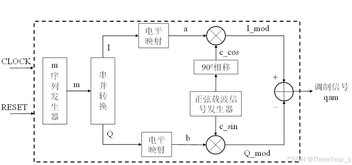
FPGA实现数字QAM调制系统要求根据正交振幅调制原理,利用正弦载波信号发生器,实现调制信号。调制原理会利用到m序列发生器,串并转换及电平映射等。
参考博客:FPGA的QAM实现
一、代码设计
整体代码框图:
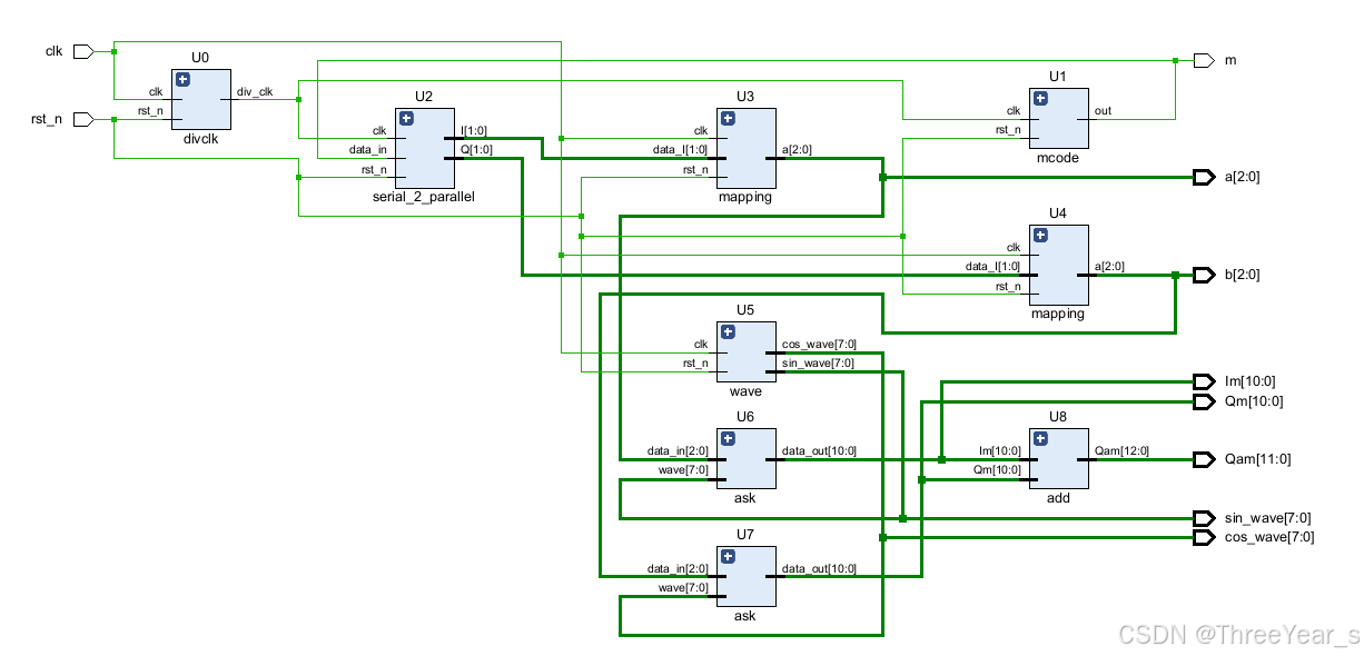
1.顶层
c
`timescale 1ns / 1ps
//////////////////////////////////////////////////////////////////////////////////
// Company:
// Engineer:
//
// Create Date: 2025/09/04 09:27:05
// Design Name:
// Module Name: qam
// Project Name:
// Target Devices:
// Tool Versions:
// Description:
//
// Dependencies:
//
// Revision:
// Revision 0.01 - File Created
// Additional Comments:
//
//////////////////////////////////////////////////////////////////////////////////


module qam(
input clk,
input rst_n,
output m,
output [2:0] a,
output [2:0] b,
output [7:0] sin_wave,
output [7:0] cos_wave,
output [10:0] Im,
output [10:0] Qm,
output [11:0] Qam
);

wire div_clk;
divclk U0(clk,rst_n,div_clk);

wire out;
mcode  U1(div_clk, rst_n, out);
assign m=out;

wire [1:0] I,Q;
serial_2_parallel  U2(div_clk, rst_n, out, I, Q);

wire [2:0] A,B;
mapping  U3(clk, rst_n, I, A);
mapping  U4(clk, rst_n, Q, B);
assign a=A;
assign b=B;

wave U5(clk, rst_n, sin_wave, cos_wave);

wire [10:0]IM,QM;
ask  U6(sin_wave, A, IM);
ask  U7(cos_wave, B, QM);
assign Im=IM;
assign Qm=QM;

add  U8(IM, QM, Qam);

endmodule
2.分频
c
`timescale 1ns / 1ps
//////////////////////////////////////////////////////////////////////////////////
// Company:
// Engineer:
//
// Create Date: 2025/09/04 09:29:55
// Design Name:
// Module Name: divclk
// Project Name:
// Target Devices:
// Tool Versions:
// Description:
//
// Dependencies:
//
// Revision:
// Revision 0.01 - File Created
// Additional Comments:
//
//////////////////////////////////////////////////////////////////////////////////


module divclk(clk,rst_n,div_clk);
input clk,rst_n;
output reg div_clk;

reg [31:0] counter;

always@(negedge rst_n or posedge clk)//计数时钟分频模块
begin
	if(!rst_n)
		begin
			counter<=32'h00000000;
			div_clk<=0;
		end
	else
		if(counter==32'h00001869)// 4KHz计数到6249翻转counter=(clk/div_clk)/2-1
			begin
				counter<=32'h00000000;
				div_clk <= ~div_clk;
				end
		else
			counter<=counter + 1;
end
endmodule
3.m序列
c
`timescale 1ns / 1ps
//////////////////////////////////////////////////////////////////////////////////
// Company:
// Engineer:
//
// Create Date: 2025/09/03 20:44:14
// Design Name:
// Module Name: mcode
// Project Name:
// Target Devices:
// Tool Versions:
// Description:
//
// Dependencies:
//
// Revision:
// Revision 0.01 - File Created
// Additional Comments:
//
//////////////////////////////////////////////////////////////////////////////////

module mcode(clk, rst_n, out);
    input clk, rst_n;   //输入端口
    output out;        //输出端口
    reg[2:0] Q;        //中间节点
    wire C0;
assign C0 =  Q[2] ^ Q[0] ;  //反馈
assign out = Q[2];           //输出信号
always@(posedge clk or negedge rst_n)
begin
    if(!rst_n )
         Q[2:0] <= 3'b111;    //异步清零,全1
    else
         Q[2:0] <= {Q[1:0],C0}; //移位
end
endmodule
4.串转并
c
`timescale 1ns / 1ps
//////////////////////////////////////////////////////////////////////////////////
// Company:
// Engineer:
//
// Create Date: 2025/09/03 20:59:35
// Design Name:
// Module Name: serial_2_parallel
// Project Name:
// Target Devices:
// Tool Versions:
// Description:
//
// Dependencies:
//
// Revision:
// Revision 0.01 - File Created
// Additional Comments:
//
//////////////////////////////////////////////////////////////////////////////////


module serial_2_parallel(clk, rst_n, data_in, I, Q);
input   clk;
input   rst_n;
input   data_in;     //序列输入
output reg[1:0] I;
output reg[1:0] Q;

reg [2:0]cnt;//计数
reg[1:0] data_I;
reg[1:0] data_Q;

always @(posedge clk or negedge rst_n)            //时序问题,第一次计数不需要进行分配。
begin
	if(!rst_n)
	begin
		I <= 2'b00;   Q <= 2'b00;
		cnt <= 3'b000;
	end

	else if(cnt==3'b100)     //4次才可以分完一组I和Q,因此分完才刷新I和Q的数据。
	begin
		I <= data_I;
		Q <= data_Q;
		cnt <= 3'b001;
	end

	else
		cnt <= cnt + 1'b1;
end

always @(*)          //串并转换
begin
                case(cnt)
	               3'b001:   data_I [1]<=data_in;
	               3'b010:   data_Q [1]<=data_in;
	               3'b011:   data_I [0]<=data_in;
	               3'b100:   data_Q [0]<=data_in;
                   default:  begin
                             data_I=2'b00;
                             data_Q=2'b00;
                             end
				endcase
end

endmodule
5.映射
c
`timescale 1ns / 1ps
//////////////////////////////////////////////////////////////////////////////////
// Company:
// Engineer:
//
// Create Date: 2025/09/03 21:15:55
// Design Name:
// Module Name: mapping
// Project Name:
// Target Devices:
// Tool Versions:
// Description:
//
// Dependencies:
//
// Revision:
// Revision 0.01 - File Created
// Additional Comments:
//
//////////////////////////////////////////////////////////////////////////////////


module mapping (clk ,rst_n ,data_I ,a);
input clk ,rst_n;
input [1:0] data_I;
output reg [2:0] a;

always@(*)
begin
            case(data_I)
	                2'b00:    a<=3'b011;
                    2'b01:    a<=3'b001;
                    2'b11:    a<=3'b111;
	                2'b10:    a<=3'b101;
                  default:    a<=3'b000;
            endcase
end

endmodule
6.正弦波余弦波生成ROM和
c
`timescale 1ns / 1ps
//////////////////////////////////////////////////////////////////////////////////
// Company:
// Engineer:
//
// Create Date: 2025/09/03 22:20:17
// Design Name:
// Module Name: wave
// Project Name:
// Target Devices:
// Tool Versions:
// Description:
//
// Dependencies:
//
// Revision:
// Revision 0.01 - File Created
// Additional Comments:
//
//////////////////////////////////////////////////////////////////////////////////


module wave(
    input clk,//50m Hz
    input rst_n,
    output [7:0] sin_wave,
    output [7:0] cos_wave
    );
parameter fre_word = 32'd858993;     //频率控制字     fre_word = f_out * 2^N / fclk   N为累加器位宽
reg [31:0] addr_sin;
wire [7:0] data1;
wire [7:0] data2;
//相位累加器
always @(posedge clk or  negedge rst_n)
begin
    if(!rst_n)
        addr_sin <= 32'b0;
    else
        addr_sin <= addr_sin + fre_word;
end

wire [11:0] addra = addr_sin[31:20];
wire [11:0] addrb = addr_sin[31:20]+1024;
//ROM IP核的调用
sin_rom sin_rom1 (
  .clka(clk),    // input wire clk	时钟
  .addra(addra),  // input wire [11 : 0] addra	相位累加器输入给rom的地址
  .douta(data1)  // output wire [7 : 0] douta	从ROM返回的数据(3M正弦波的采样点)
);

sin_rom cos_rom1 (
  .clka(clk),    // input wire clk	时钟
  .addra(addrb),  // input wire [11 : 0] addra	相位累加器输入给rom的地址
  .douta(data2)  // output wire [7 : 0] douta	从ROM返回的数据(3M正弦波的采样点)
);

assign sin_wave = data1-128;
assign cos_wave = data2-128;
endmodule
7.ask
c
`timescale 1ns / 1ps
//////////////////////////////////////////////////////////////////////////////////
// Company:
// Engineer:
//
// Create Date: 2025/09/04 08:57:12
// Design Name:
// Module Name: ask
// Project Name:
// Target Devices:
// Tool Versions:
// Description:
//
// Dependencies:
//
// Revision:
// Revision 0.01 - File Created
// Additional Comments:
//
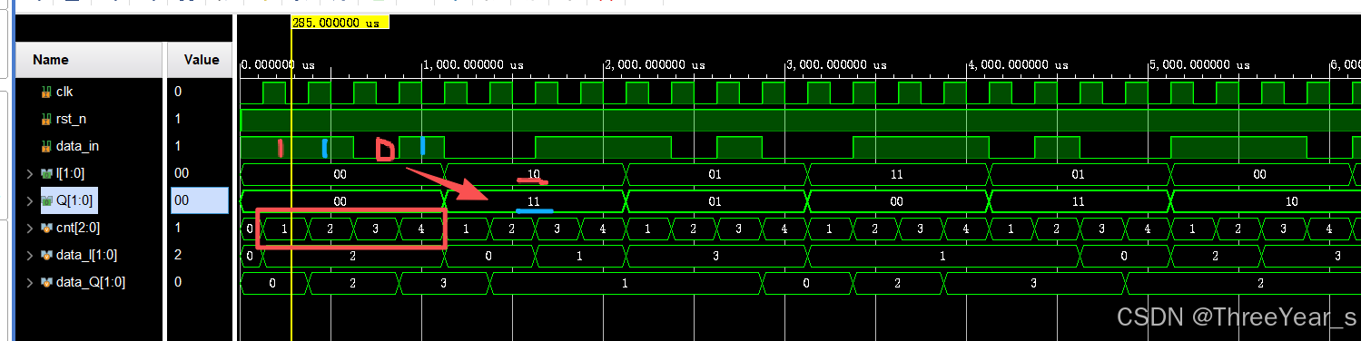
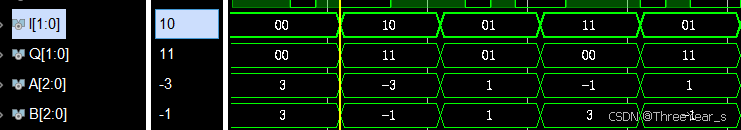
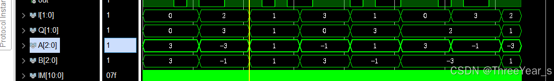
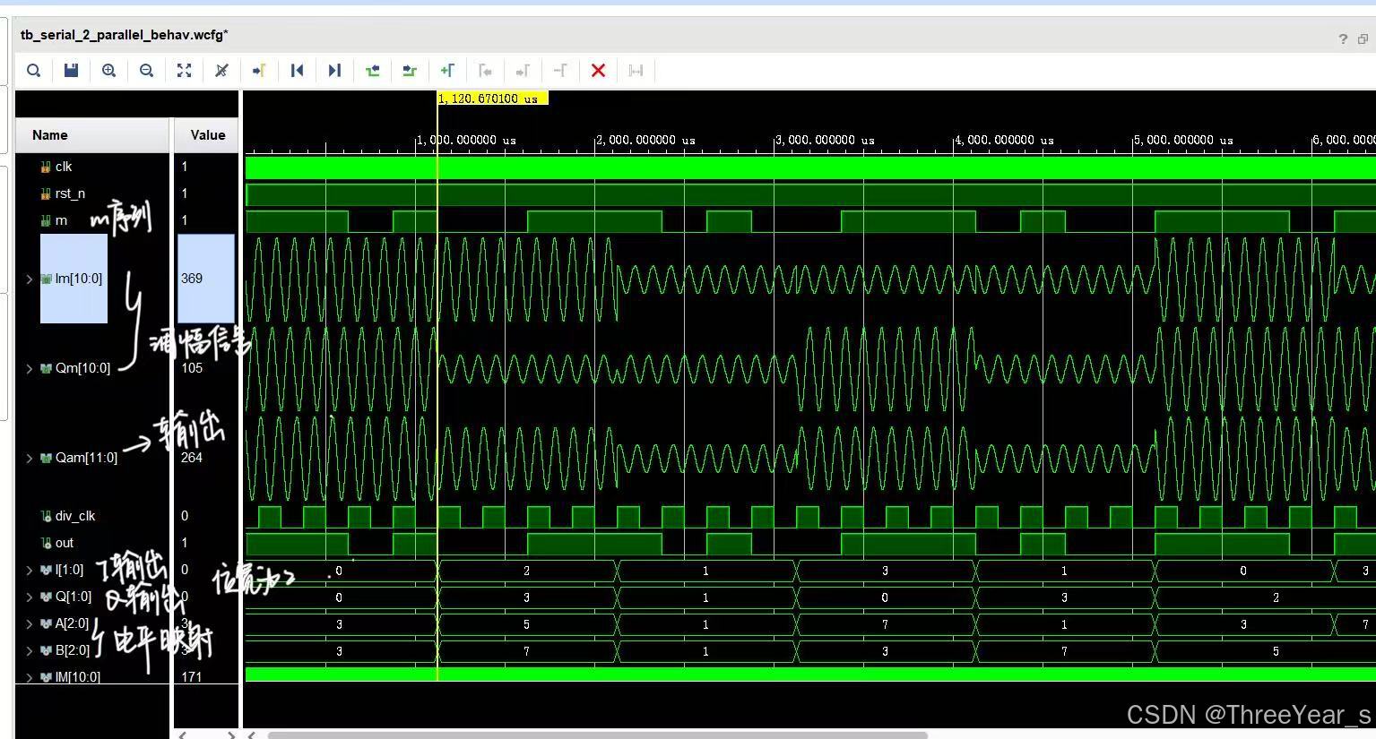
//////////////////////////////////////////////////////////////////////////////////二、仿真波形
总结
结合文章代码进行复现。