相关阅读
物理约束命令![]() https://blog.csdn.net/weixin_45791458/category_13122483.html
https://blog.csdn.net/weixin_45791458/category_13122483.html
在Design Compiler:物理约束一文中,已经提到在第一轮综合时,用户可以使用自定义物理约束,本文就将介绍如何使用这些命令创建芯片(Die)区域和核心(Core)区域。
芯片(Die)区域是整个芯片在硅片上的物理边界,包含核心区域、I/O PAD等所有结构,是芯片的总面积;而核心(Core)区域是芯片内部专门用于放置标准单元和宏单元的逻辑布局区域,不包含I/O PAD等外围电路,芯片(Die)区域包含核心(Core)区域,如图1所示。
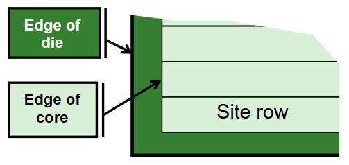
图1 芯片(Die)区域和核心(Core)区域
相对定义
如果用户未显式创建芯片(Die)区域和核心(Core)区域,Design Compiler将使用默认的物理约束,即长宽比为1(即正方形)和单元利用率为0.6,单元利用率的定义如下所示。
图2展示了一个综合结果的版图,其中绿色线表示的既是是芯片(Die)区域也是核心(Core)区域。
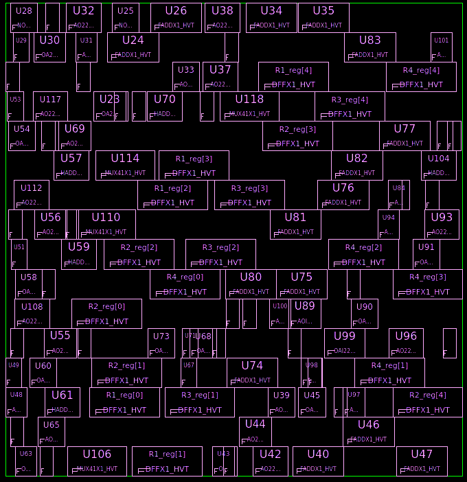
图2 综合结果的版图
可以使用report_area -physical命令报告设计的长宽比和单元利用率,如下所示。
dcnxt_shell-topo> report_area -physical

****************************************
Report : area
Design : MY_DESIGN
Version: W-2024.09-SP2
Date   : Mon Jan 26 21:26:14 2026
****************************************

Library(s) Used:

    saed32hvt_ss0p95v125c (File: /home/zhangchen/DCNXT_2021.06/bug/saed32hvt_ss0p95v125c.db)

Number of ports:                           42
Number of nets:                           144
Number of cells:                          114
Number of combinational cells:             94
Number of sequential cells:                19
Number of macros/black boxes:               0
Number of buf/inv:                         25
Number of references:                      16

Combinational area:                257.447871
Buf/Inv area:                       31.768000
Noncombinational area:             125.547140
Macro/Black Box area:                0.000000
Net Interconnect area:      undefined  (Wire load has zero net area)

Total cell area:                   382.995012
Total area:                 undefined

Core Area:                       679
Aspect Ratio:                 1.0539
Utilization Ratio:            0.5640


The above information was reported from the logical library. The following are from the physical library:

  Total moveable cell area: 383.0
  Total fixed cell area: 0.0
  Total physical cell area: 383.0
 Core area: 0.000, 0.000, 25.384, 26.752
用户可以使用set_aspect_ratio命令和set_utilization命令设置设计的长宽比和单元利用率,如下所示。
dcnxt_shell-topo> set_aspect_ratio 0.5
dcnxt_shell-topo> set_utilization 0.8
此时综合结果的的版图如图3所示,其中绿色线表示的既是是芯片(Die)区域也是核心(Core)区域。
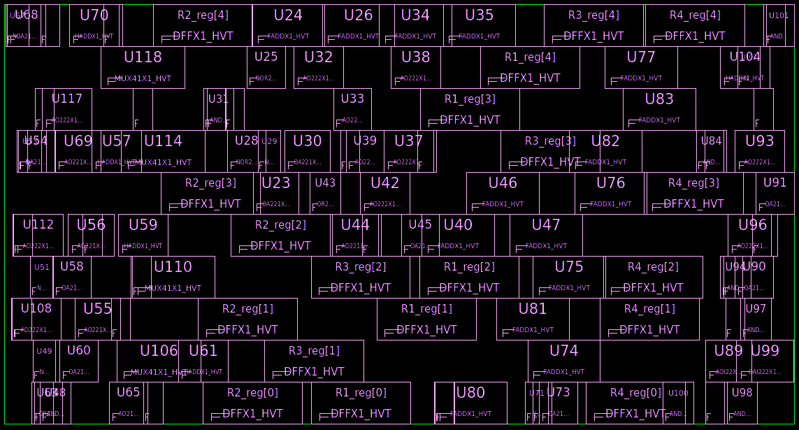
图3 综合结果的版图
可以使用report_area -physical命令报告设计的长宽比和单元利用率,如下所示。Design Compiler将尽量让单元利用率接近但不大于设置值。
dcnxt_shell-topo> report_area -physical

****************************************
Report : area
Design : MY_DESIGN
Version: W-2024.09-SP2
Date   : Mon Jan 26 21:49:08 2026
****************************************

Information: Updating design information... (UID-85)
Library(s) Used:

    saed32hvt_ss0p95v125c (File: /home/zhangchen/DCNXT_2021.06/bug/saed32hvt_ss0p95v125c.db)

Number of ports:                           42
Number of nets:                           148
Number of cells:                          118
Number of combinational cells:             98
Number of sequential cells:                19
Number of macros/black boxes:               0
Number of buf/inv:                         27
Number of references:                      17

Combinational area:                264.563903
Buf/Inv area:                       34.309440
Noncombinational area:             125.547140
Macro/Black Box area:                0.000000
Net Interconnect area:      undefined  (Wire load has zero net area)

Total cell area:                   390.111043
Total area:                 undefined

Core Area:                       526
Aspect Ratio:                 0.5314
Utilization Ratio:            0.7415


The above information was reported from the logical library. The following are from the physical library:

  Total moveable cell area: 390.1
  Total fixed cell area: 0.0
  Total physical cell area: 390.1
 Core area: 0.000, 0.000, 31.464, 16.720
绝对定义
上一节的相对定义约束并没有显式指定芯片(Die)区域和核心(Core)区域,本节将介绍几个绝对定义约束,注意这些绝对定义约束的优先级大于相对定义约束。
create_die_area
create_die_area命令用于创建一个芯片(Die)区域,使用-coordinate选项可以创建一个四边形的芯片(Die)区域,使用-coordinate选项可以创建一个直角多边形的芯片(Die)区域。
如果只创建了芯片(Die)区域而没有创建核心(Core)区域,则芯片(Die)区域会被视为核心(Core)区域,下面展示了一个例子。
dcnxt_shell-topo> create_die_area -polygon {{0 0} {0 30} {20 30} {20 20} {30 20} {30 0}}此时综合结果的的版图如图4所示,其中绿色线表示的既是是芯片(Die)区域也是核心(Core)区域。
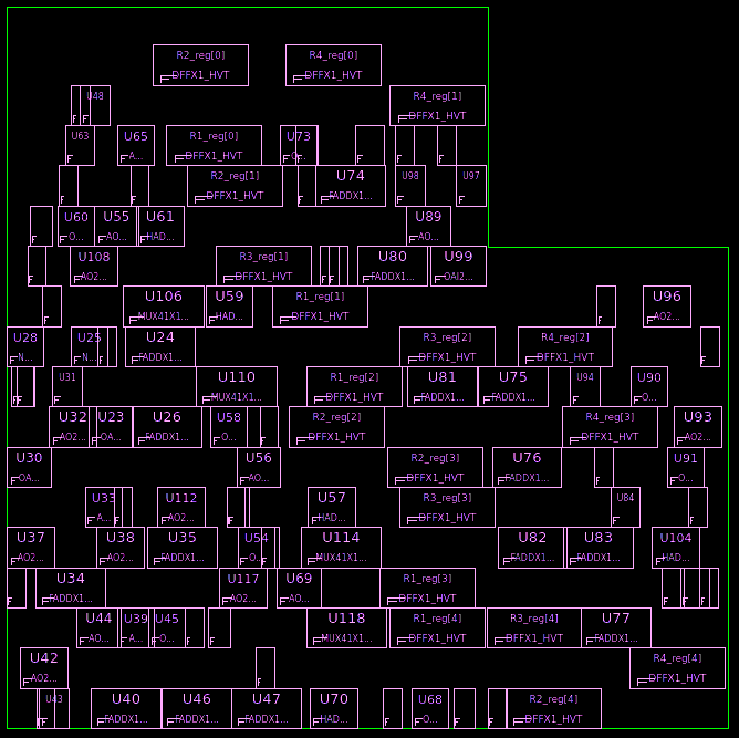
图4 综合结果的版图
如果芯片(Die)区域已存在,再次使用create_die_area命令时会出现以下错误。
Error: Die area already exists in the design. (DCT-064)create_core_area(不建议使用)
create_core_area命令用于创建一个核心(Core)区域,使用-coordinate选项可以创建一个四边形的核心(Core)区域。
如果只创建了核心(Core)区域而没有创建芯片(Die)区域,则核心(Core)区域会被视为芯片(Die)区域,下面展示了一个例子。
dcnxt_shell-topo> create_core_area -coordinate {{0 0} {30 30}}此时综合结果的的版图如图5所示,其中绿色线表示的既是是芯片(Die)区域也是核心(Core)区域。
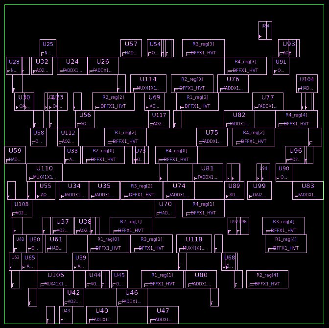
图5 综合结果的版图
create_core_area命令配合create_die_area命令可以完整创建芯片(Die)区域和核心(Core)区域,下面展示了一个例子。
dcnxt_shell-topo> create_die_area -coordinate {{0 0} {50 50}}
dcnxt_shell-topo> create_core_area -coordinate {{0 0} {30 30}}此时综合结果的的版图如图6所示,其中绿色线表示的是核心(Core)区域,蓝色线表示的是芯片(Die)区域。
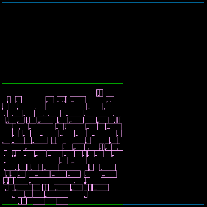
图6 综合结果的版图
如果核心(Core)区域已存在,再次使用create_core_area命令时会出现以下错误。
Error: Core area already exists in the design. (DCT-063)该命令已经不建议使用了,如果想创建核心(Core)区域,使用create_site_row命令创建site row。
create_site_row
create_site_row命令可用于创建site row,核心(Core)区域即为包含所有site row的四边形区域,下面展示了一个例子。
dcnxt_shell-topo> create_die_area -coordinate {{0 0} {40 25}}
dcnxt_shell-topo> create_site_row -name unit0 -coordinate {10 11.672} -kind unit -space 0.152 -count 100
dcnxt_shell-topo> create_site_row -name unit1 -coordinate {10 13.344} -kind unit -space 0.152 -count 100
dcnxt_shell-topo> create_site_row -name unit2 -coordinate {10 13.344} -kind unit -space 0.152 -count 100此时综合结果的的版图如图7所示(为了简便,这里使用了一个只包含一个标准单元的设计),其中红色线表示的是三行site row,绿色线表示的是核心(Core)区域,蓝色线表示的是芯片(Die)区域。
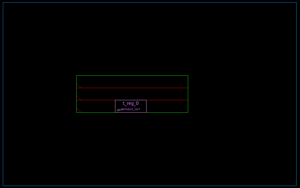
图7 综合结果的版图
set_placement_area
set_placement_area命令用于创建或设置芯片(Die)区域和核心(Core)区域,当芯片(Die)区域不存在时,创建芯片(Die)区域,当芯片(Die)区域存在且是由本命令创建的时,设置芯片(Die)区域,当核心(Core)区域不存在时,创建核心(Core)区域,当核心(Core)区域存在时,设置核心(Core)区域。
该命令只能使用-coordinate选项创建或设置一个四边形的芯片(Die)区域和核心(Core)区域。
set_rectilinear_outline(不建议使用)
set_rectilinear_outline命令用于创建或设置芯片(Die)区域,当芯片(Die)区域不存在时,创建芯片(Die)区域,当芯片(Die)区域存在时,设置芯片(Die)区域。
该命令只能使用-coordinate选项创建或设置一个直角多边形的芯片(Die)区域。