Flip chip (FC) technology is a packaging method in which the chip is directly attached to the substrate, which has the advantages of high density, high performance and low cost. However, due to the coefficient of thermal expansion (CTE) mismatch between the chip and the substrate, the solder joints are subjected to large thermal stresses when the temperature changes, leading to fatigue damage and failure. To improve the reliability of solder joints, a common method is to inject a polymer material, called underfill, between the chip and the substrate. Underfill improves the stress distribution in the solder joint, reduces the strain amplitude in the solder joint, and extends the thermal fatigue life of the solder joint.
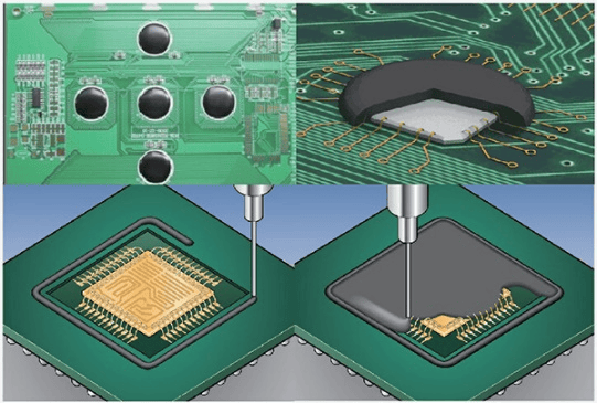
Figure 1. Underfill process
Underfill is a liquid encapsulant, typically an epoxy resin heavily filled with SiO2, that is used between the chip and the substrate after flip chip interconnections. After curing, the hardened underfill has a high modulus, low CTE to match the solder joints, low moisture absorption, and good adhesion to the chip and substrate. Thermal stresses on the solder joints are redistributed between the chip, underfill, substrate and all solder joints, rather than being concentrated on the peripheral solder joints. The application of underfill has been proven to reduce the most important solder joint strain levels to 0.10-0.25 of the strain of an unencapsulated solder joint. as a result, underfill can increase the fatigue life of solder joints by a factor of 10 to 100. In addition, it protects the solder joints from environmental attack. Underfill is a practical solution for expanding the use of flip chip technology from ceramic to organic substrates and from high-end to cost-sensitive products.

Figure 2. Flip Chip Process with Underfill
Advances in flip chip technology have led to the development of underfill processes and underfill materials. Figure 2 illustrates the process steps of a flip chip using the underfill process. Separate flux dispensing and cleaning steps are required before and after the chip is assembled. After the chip is assembled on the substrate, the unfilled material is dispensed and dragged into the gap between the chip and the substrate.
Foreign material control before underfill application
Bottom filler adhesive before sizing need to confirm that the board and filler surface without foreign objects and a large number of flux residue, more flux residue will lead to adhesive attached to the flux residue, subsequent use of the process of flux residue volatilization, softening, mutation directly affect the mechanical properties of the adhesive, which affects the reliability of the product. The standard bottom filling sizing process requires PCBA cleaning and drying, and then dispensing curing.
The advantages of the bottom filling process are:
-
Improve the reliability of the solder joints to extend the service life of the product;
-
Protect the solder joints from environmental erosion, improve product corrosion resistance;
-
Reduce the thermal stress between the chip and the substrate, improve the product's resistance to thermal cycling;
-
Enhance the adhesion between the chip and the substrate to improve the impact resistance and vibration resistance of the product.
Disadvantages of the bottom filling process:
-
Increase the cost and complexity of packaging, requiring additional equipment and materials;
-
Need to select appropriate bottom-filling materials and parameters to match the characteristics of the chip and substrate to avoid failure modes such as residual stress, cracks, corrosion and voids;
-
Difficult to repair or rework the package, requiring the removal of the bottom filler in order to inspect or replace the solder joints;
-
may affect the electrical properties of the chip, such as signal delay, crosstalk, noise, etc..
Translated with DeepL.com (free version)