目录
1.bit流压缩
set_property BITSTREAM.GENERAL.COMPRESS TRUE current_design
2.flash加载速度
打开bitstream setting,设置SPI的线宽和速率(线宽按原理图设置,速率尽可能高)
3.Tandem模式
Overview
PCIe requires a link training within 120ms after power is stable. This can be a challenging phase of programming FPGA devices due to the size of the bitstream to program the FPGA and the rate of configuration available. Therefore, the Tandem PCIe feature is used to address this challenge.
The Tandem PCIe contains two stages of bitstream. The first stage includes the programming of the necessary memory cells for the PCIe loaded from the Programmable Read Only Memory (PROM). Afterwards, the PCIe port is capable of handling and responding to enumerations. In parallel, the second stage bitstream is transmitted via the PCIe link. The second stage bitstream contains the user application that can be configured using the Media Configuration Access Port (MCAP). Please refer to (Answer Record 64761).
See the figure below for the load steps.
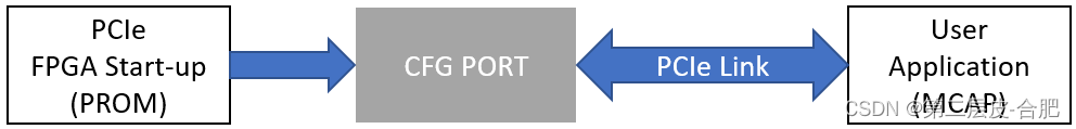
Figure 1 - Tandem PCIe Bitstream Load Steps
This blog provides a step-by-step guide on how to use the Tandem PCIe feature on a KCU116 board.
Tandem PCIe Design Flow
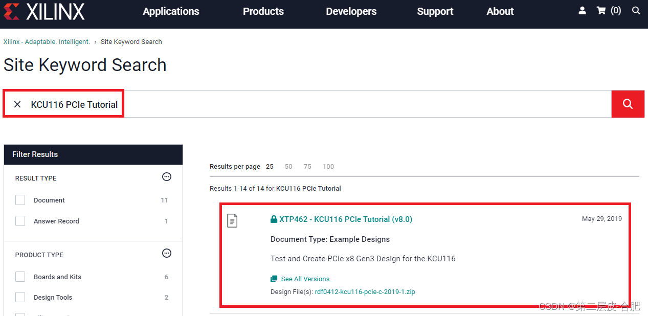
On the AMD website, search for the KCU116 PCIe Tutorial and download the latest version for the example design.
Click on "XTP642 -- KCU116 PCIe Tutorial (v8.0)" to view the PDF slides for creating an example PCIe design. Click on "rdf0412-kcu116-pcie-c-2019-1.zip" to download the design files.
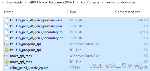
Extract the contents of "ready_for_download" from the downloaded design file to the C:\ drive or your preferred directory.
Configure the following settings in the "Basic " tab. Leave the default "Component Name".
Change the "Mode" to Advanced to unlock all of the features of the IP. Make sure the "Device/Port Type" is PCI Express Endpoint device and the "PCIe Block Location" is at X0Y0 . Change the "Lane Width" to X1 or depending on user specification and the "Maximum Link Speed" to 8.0 GT/s (Gen3). Check the "Reference Clock Frequency (MHz)" is set to 100MHz . Select Tandem PCIe from "Tandem Configuration or Partial Reconfiguration".