一、Chirp生成模块介绍
采用Verilog 生成Chirp,实现输入使能电平,模块输出Chirp信号,Chirp信号频率范围,时间宽度,连续Chirp信号数量可配置。
二、模块例化方法示例
parameter     FL	 ='d20_000 		;
parameter     FH	 ='d30_000 		;
parameter     Tc	 ='d10			;  //ms
parameter   Chirp_Num='d128;
chirp
#(
	.  SYS_CLK	(SYS_CLK),
	.  FL	 	(FL),
	.  FH	 	(FH),
	.  Tc	 	(Tc), //ms
	.  Chirp_Num(Chirp_Num)
)
chirp_inst
(
	 .   	sys_clk		(clk_9_6m),
	 .  	rst_n		(rst_n),
	 .  	chirp_en	(chirp_en),

	 .  	chirp_out	(chirp_out),
	 .		chirp_valid	(chirp_valid),
	 .		chirp_index (chirp_index)
 );
三、模块仿真时序图
 四、模块代码
`timescale 1ns / 1ps
//
// Company:
// Engineer: YOU
//
// Create Date: 2023/10/25 10:11:24
// Design Name:
// Module Name: Chirp
// Project Name:
// Target Devices:
// Tool Versions:
// Description:
//
// Dependencies:
//
// Revision:
// Revision 0.01 - File Created
// Additional Comments:
//
//
module chirp_cp
#(
parameter SYS_CLK='d6_400_000,
parameter FL ='d22_400 ,
parameter FH ='d28_800 ,
parameter Tc ='d20 ,//ms
parameter Chirp_Num='d128
)
(
input wire sys_clk,
input wire rst_n,
input wire chirp_en,
output wire [7:0] chirp_out,
output wire chirp_valid,
output reg [19:0] chirp_index
);
parameter B =FH-FL;
parameter K =B*1000/Tc;
parameter T_MAX=SYS_CLK*Tc/1000; // t/SYS_CLK 单位为s
reg [7:0] chirp_cnt;
reg [39:0] t;
reg [39:0] t_dl;
always@(posedge sys_clk or negedge rst_n)
if(!rst_n)
chirp_cnt<='d0;
else if(chirp_en==1'b1)
chirp_cnt<='d0;
else if(t==T_MAX+1'b1)
chirp_cnt<=chirp_cnt+1'b1;
else
chirp_cnt<=chirp_cnt;
always@(posedge sys_clk or negedge rst_n)
if(!rst_n)
t<='d0;
else if(t==T_MAX+1'b1&&chirp_cnt>=Chirp_Num-1)
t<='d0;
else if(t==T_MAX+1'b1&&chirp_cnt<Chirp_Num-1)
t<='d2;
else if(chirp_en==1'b1)
t<=t+1'b1;
else if(t>=1'b1)
t<=t+1'b1;
else
t<='d0;
//t_dl
always@(posedge sys_clk or negedge rst_n)
if(!rst_n)
t_dl<='d0;
else
t_dl<=t;
wire [79:0] t_2;
chirp_mul chirp_mul_inst (
.CLK(sys_clk), // input wire CLK
.A(t), // input wire [39 : 0] A
.B(t), // input wire [39 : 0] B
.P(t_2) // output wire [79 : 0] P
);
reg [15:0] phase_reg;
//phase_reg
always@(posedge sys_clk or negedge rst_n)
if(!rst_n)
phase_reg<='d0;
else
phase_reg<=2*FL*32768*t_dl/SYS_CLK+K*32768*t_2/SYS_CLK/SYS_CLK; //由于cordic输入为fix16_13 ,所以乘上2^13,就能获得fix16_13数据
reg [15:0] phase;
//phase
always@(posedge sys_clk or negedge rst_n)
if(!rst_n)
phase<='d0;
else if(phase_reg[15:15]=='b0)
phase<=(phase_reg+1'b1)>>2; //将-32767~32767 对应 -pi~pi 转为000.00000 形式取值范围为-1~1 单位为pi
else
phase<=(phase_reg>>2)+16'b1100_0000_0000_0000; //这个右移两位,高位补一能实现,负数到fix16_13形式的转换
reg chirp_cordic_en;
always@(posedge sys_clk or negedge rst_n)
if(!rst_n)
chirp_cordic_en<=1'b0;
else if(t>=2&&t<=T_MAX+1'b1)
chirp_cordic_en<=1'b1;
else
chirp_cordic_en<=1'b0;
wire [15:0] chirp_data;
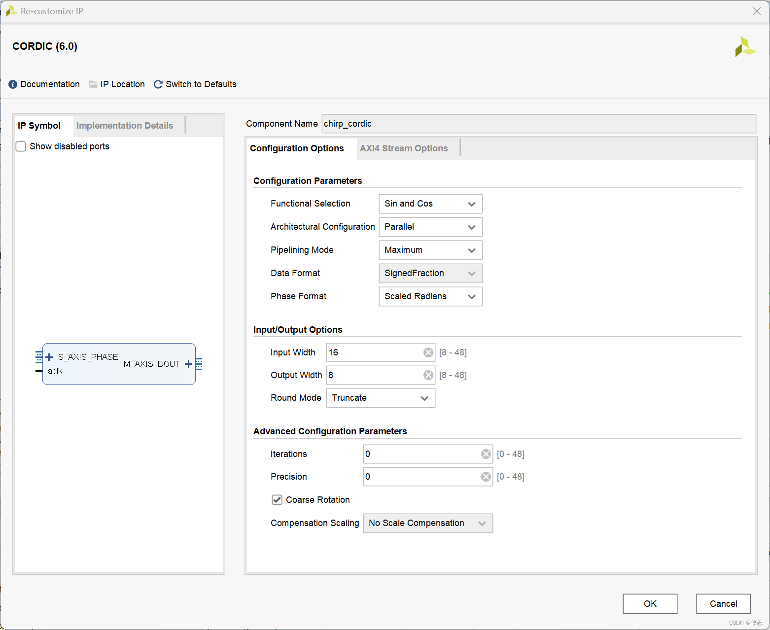
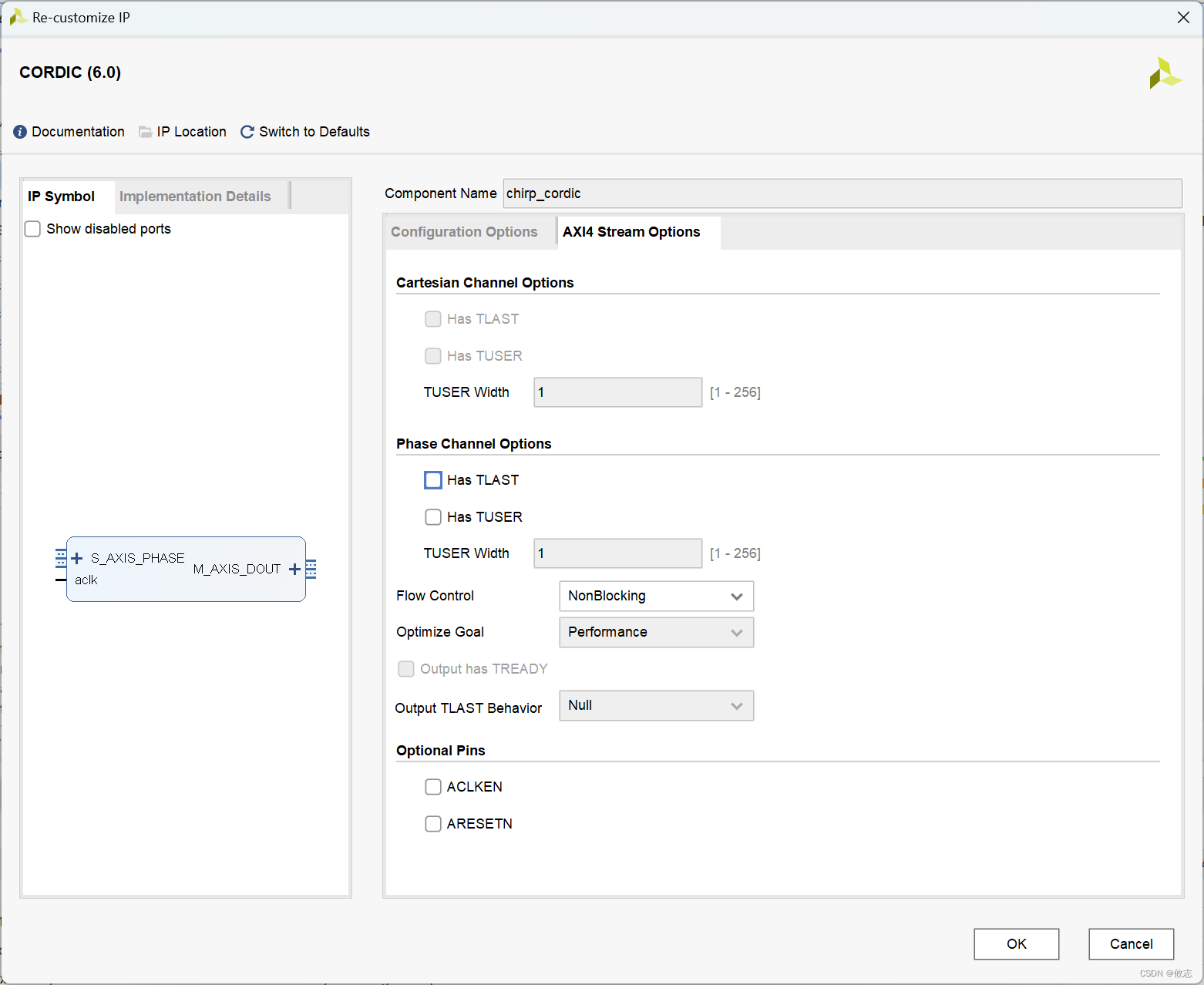
chirp_cordic chirp_cordic_inst (
.aclk(sys_clk), // input wire aclk
.s_axis_phase_tvalid(chirp_cordic_en), // input wire s_axis_phase_tvalid
.s_axis_phase_tdata(phase), // input wire [15: 0] s_axis_phase_tdata
.m_axis_dout_tvalid(chirp_valid), // output wire m_axis_dout_tvalid
.m_axis_dout_tdata(chirp_data) // output wire [15 : 0] m_axis_dout_tdata
);
assign chirp_out=chirp_data[7:0];
//chirp_index
always@(posedge sys_clk or negedge rst_n)
if(!rst_n)
chirp_index<='d0;
else if(chirp_valid==1'b1)
chirp_index<=chirp_index+1'b1;
else
chirp_index<='d0;
endmodule五、模块相关IP核配置(vivado)
六、总结
以上内容介绍,基于FPGA实现的可配置参数的chirp信号生成模块使用以及代码,如果确实有帮助到大家谢谢点赞支持。