1 PWM 简介


2 F28335的ePWM介绍


2.1 时基模块TB


(1)时基模块的功能
(2)时基模块的关键信号和寄存器
给出时基模块内部结构图来了解里面的关键信号和寄存器,时基模块内部结构图如下所示:


(3)计算ePWM 周期和频率
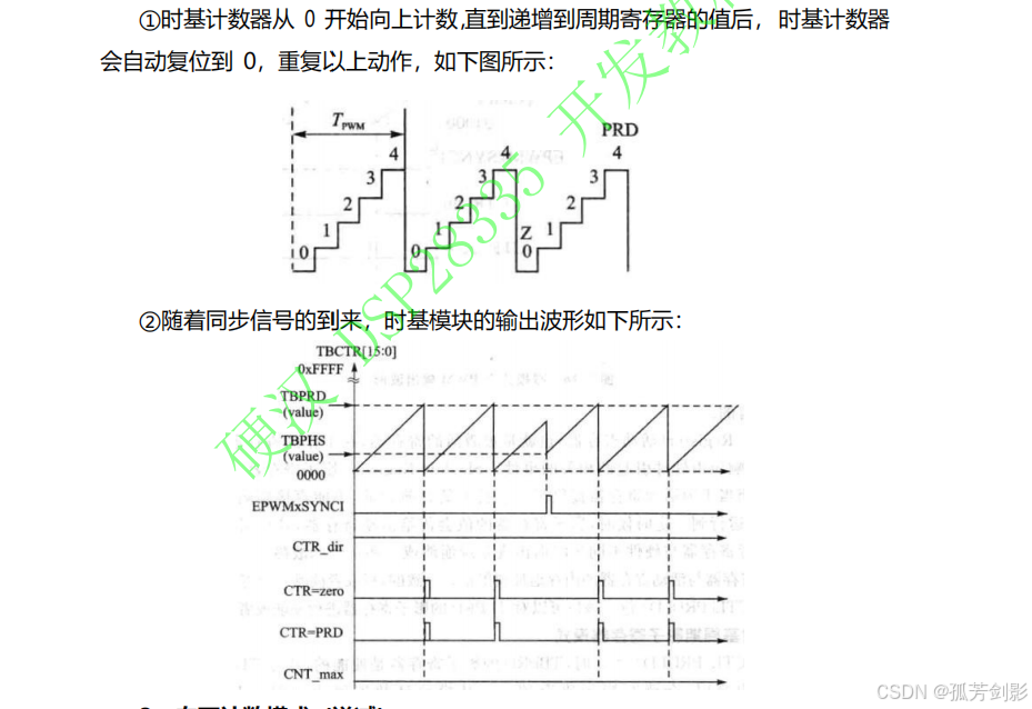
1、向上-向下计数模式(先递增后递减)


2、向上计数模式(递增)
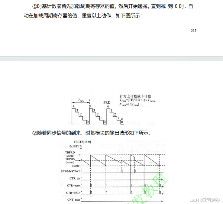
3、向下计数模式(递减)
(4)影子寄存器


2.2 计数比较模块CC


(1)计数器比较模块 CC 的功能
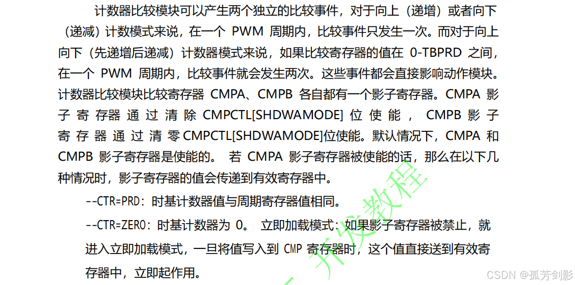
(2)计数器比较模块 CC 的关键信号与寄存器


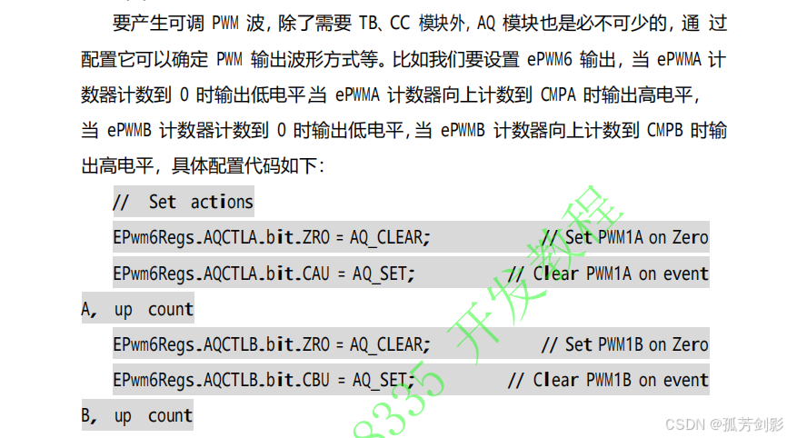
2.3 动作限定模块AQ
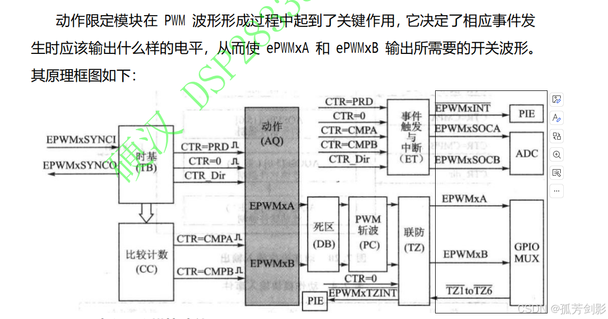
(1)动作限定模块功能
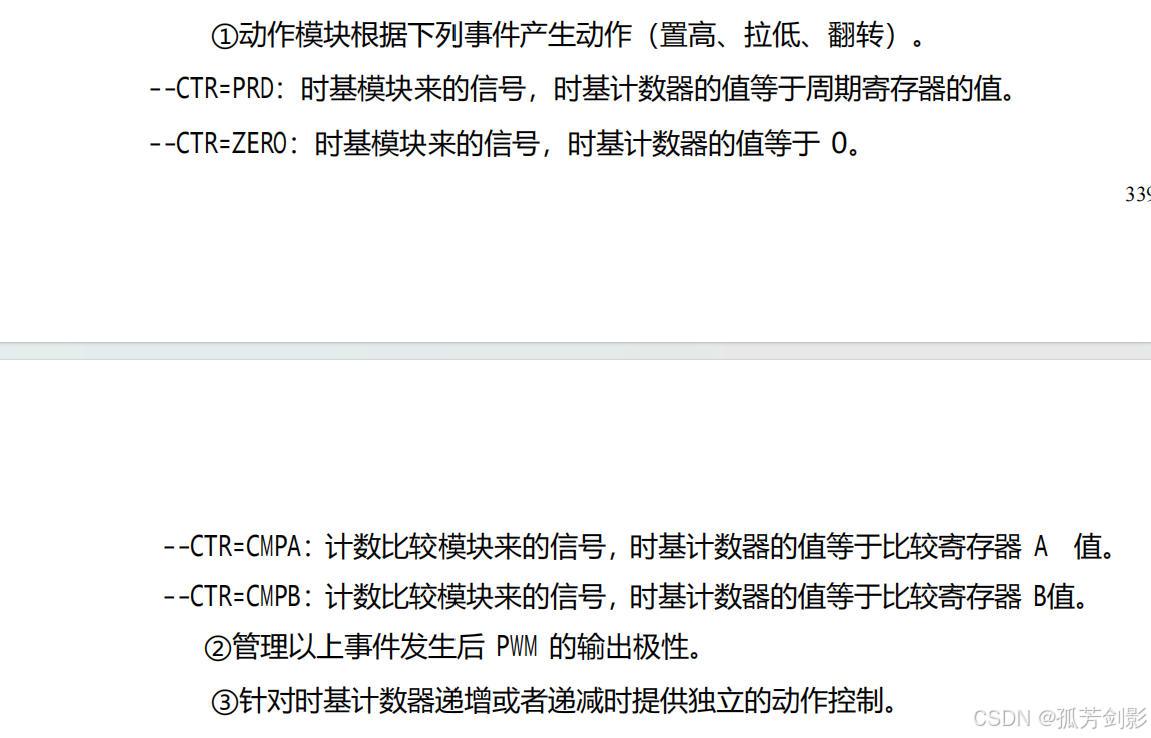
(2)动作限定模块关键信号与寄存器


(3) 动作限定模块事件优先级


最高同样是软件强制,最低是计数器等于周期寄存器的值匹配事件。
(4)动作限定模块一般配置条件下的输出波形


注意:
①PWM 周期=(TBPRD+1)*T(TBCLK)
②CMPA 决定 ePWMxA 的占空比,CMPB 决定 ePWMxB 占空比。
下面是该输出波形相关配置代码:
c
EPwm6Regs.TBPRD = tbprd;//设定 PWM 周期为 tbprd+1 个 TBCLK 时钟周期
EPwm6Regs.CMPA.half.CMPA = 350;//比较器 A 的值为 350
EPwm6Regs.CMPB = 200;//比较器 B 的值为 200
EPwm6Regs.TBPHS.half.TBPHS = 0;//相位寄存器清零
EPwm6Regs.TBCTR = 0x0000;//时基计数器清零
EPwm6Regs.TBCTL.bit.CTRMODE = TB_COUNT_UP;//设定为增计数模式
EPwm6Regs.TBCTL.bit.PHSEN = TB_DISABLE;//禁止相位控制
EPwm6Regs.TBCTL.bit.PRDLD = TB_SHADOW;//TBPRD 寄存器采用影子寄存器模式
EPwm1Regs.TBCTL.bit.SYNCOSEL = TB_SYNC_DISABLE;//禁止同步信号
EPwm6Regs.TBCTL.bit.HSPCLKDIV=TB_DIV1;//设定 TBCLK=SYSCLK 时基时钟=系统时钟
EPwm6Regs.TBCTL.bit.CLKDIV=TB_DIV1;

EPwm6Regs.CMPCTL.bit.SHDWAMODE = CC_SHADOW;//设定 CMPA 为影子寄存器 模式
EPwm6Regs.CMPCTL.bit.SHDWBMODE = CC_SHADOW;
EPwm6Regs.CMPCTL.bit.LOADAMODE = CC_CTR_ZERO;//在 CTR=Zero 时装载
EPwm6Regs.CMPCTL.bit.LOADBMODE = CC_CTR_ZERO;
EPwm6Regs.AQCTLA.bit.ZRO = AQ_SET;//CTR=ZERO 时,将 ePWM6A 置高
EPwm6Regs.AQCTLA.bit.CAU = AQ_CLEAR;//CTR=CAU 时,将 ePWM6A 置低
EPwm6Regs.AQCTLB.bit.ZRO = AQ_SET;//CTR=ZERO 时,将 ePWM6B 置高
EPwm6Regs.AQCTLB.bit.CBU = AQ_CLEAR;//CTR=CAU 时,将 ePWM6B 置低
EPwm6Regs.CMPA.half.CMPA = Duty1A;//调整 ePWM6A 的占空比
EPwm6Regs.CMPB = Duty1B;//调整 ePWM6B 的占空比


2.4 死区控制模块DB
ePWM中的死区控制子模块DB就是用来严格地控制死区产生的边沿和极性。死区控制子模块在整个ePWM模块中的位置如图所示。

(1)为什么要产生死区


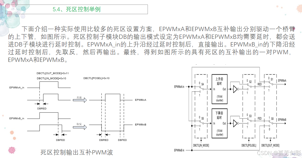
(2)死区控制模块的作用
F28335 的死区模块主要作用就是让两个互补的对称的 PWM 波形中,上升沿的

(3)死区控制模块的特点


(4)举例
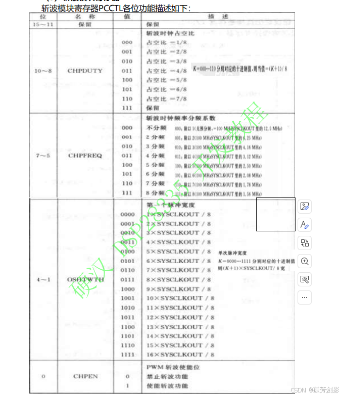
2.5 PWM 斩波模块PC
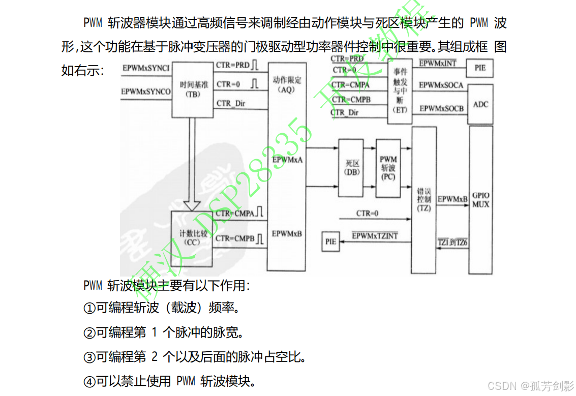
在使用ePWM模块的过程中如果无须用到此功能,可通过相关寄存器完全屏蔽该子模块,从而使PWM 脉冲直接通过。
(1)PWM 斩波模块的特点
如果信号不需要通过斩波控制子模块而直接输出,只需将PCCTLCHPEN置0就可以。若将PCCTLCHPEN置1,则斩波功能使能,PWM信号将经过高频载波信号调制后再输出。


(2)单次脉冲
原先PWM高电平的地方变成了高频载波信号,把每一个周期内的第一个载波脉冲称为首次脉冲(one shot)。首次脉冲的宽度是可编程的,可以使得第一个脉冲携带较大的能量,从而保证功率器件能够可靠开通,而其余脉冲用来维持功率器件的持续开通与关断。


2.6 错误联防模块 TZ
每个 ePWM 模块都与 GPIO 多路复用引脚中的 6 个 TZn(TZ1-TZ6)信号脚连接。
这些信号脚用来响应外部错误或外部触发条件,当错误发生时,PWM 模块可以通 过
编程来响应这些问题。错误联防模块的位置如下图所示:

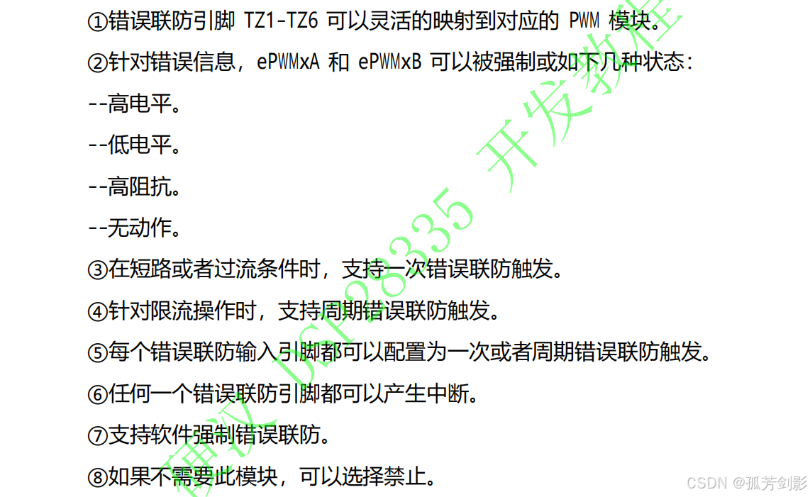
(1)错误联防模块的主要作用如下:
(2)故障捕获子模块内部逻辑图
通过选择寄存器TZSEL,每个ePWM模块都可以使用或者忽略6路故障触发信号中的任何一路,如果某个ePWM不使用故障保护的功能,也就是忽略了所有的故障触发信号,那么这个ePWM模块的PWM信号不受故障保护,将直接输出。如果为某个ePWM模块选择了故障触发信号输入引脚,该引脚平时是高电平状态,如果通过电路的设计,外部一旦出现故障,将该故障触发信号输入引脚的电平置为低电平,则故障捕获子模块捕获到故障信号,然后根据控制寄存器TZCTL的设置来完成相应的动作,可以将相应的EPWMxA引脚和EPWMxB引脚强制为低电平、高电平或者高阻态输出。
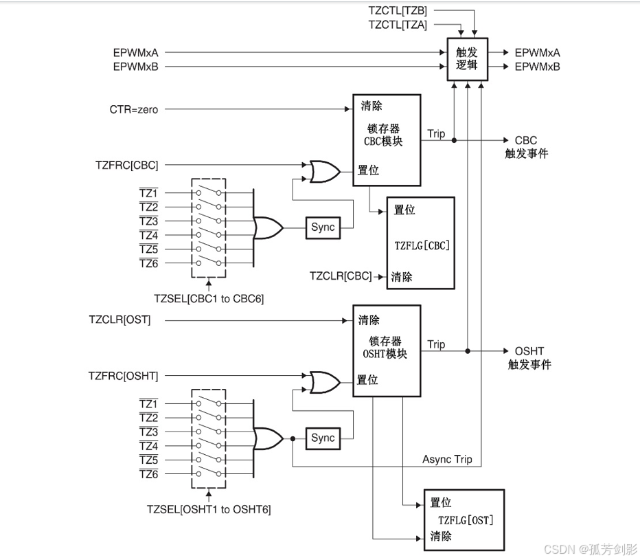
(3)错误联防模块的操作


2.7 事件触发模块
事件触发子模块(ET)用来处理时间基准计数器、比较功能子模块所产生的事件,从而向CPU发出中断请求或产生ADC启动信号SOCA或SOCB。


2.8 PWM模块相关寄存器
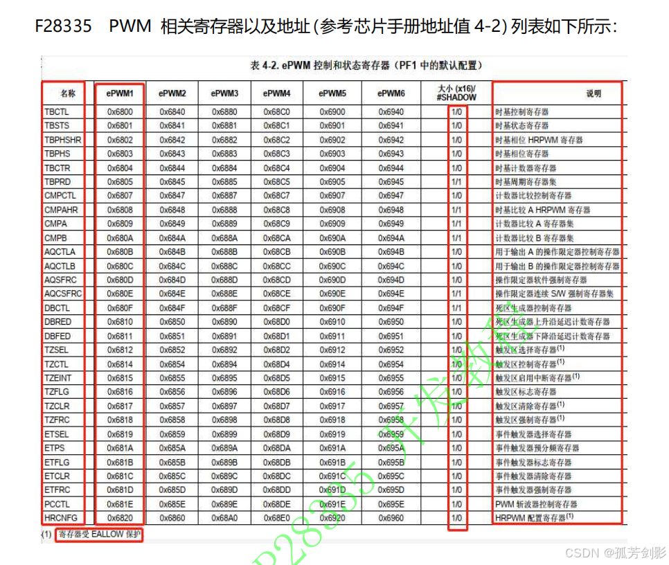
(1)时基模块相关寄存器


(2)计数比较模块寄存器


(3)动作模块寄存器


(4)死区模块寄存器


(5)斩波模块寄存器
(6)错误联防模块寄存器


(7)事件触发模块寄存器


3 PWM 输出配置步骤
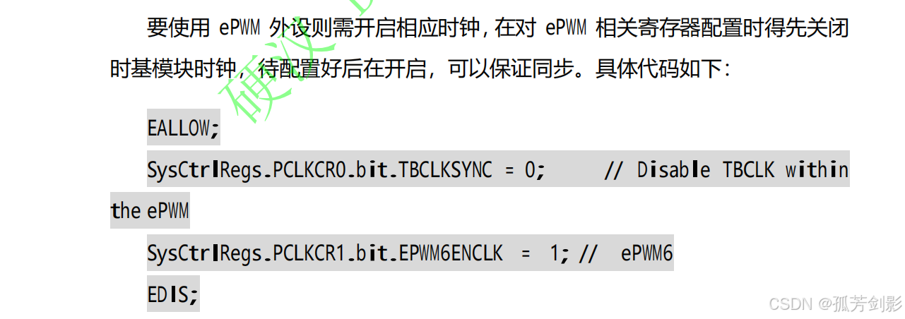
(1)使能 ePWM 外设时钟及使能时基模块时钟
(2)开启 ePWM 对应 GPIO 时钟及初始化配置
由于 PWM 输出通道是对应着 F28335 芯片的 IO 口,所以需要使能对应的端口 时钟,并将对应 IO 口配置为 ePWM 输出功能。初始化 ePWM GPIO 的函数 TI已经提供给我们了,直接调用即可。本章使用的是 ePWM6,调用的函数如下:
c
InitEPwm6Gpio();
//其内部具体实现代码如下:
void InitEPwm6Gpio(void)
{
EALLOW;
/* Enable internal pull-up for the selected pins */
// Pull-ups can be enabled or disabled by the user.
// This will enable the pullups for the specified pins.
// Comment out other unwanted lines. GpioCtrlRegs.GPAPUD.bit.GPIO10 = 0; // Enable pull-up on
GPIO10 (EPWM6A)
GpioCtrlRegs.GPAPUD.bit.GPIO11 = 0; // Enable pull-up on
GPIO11 (EPWM6B)
/* Configure ePWM-6 pins using GPIO regs*/
// This specifies which of the possible GPIO pins will be ePWM6 functional pins.
// Comment out other unwanted lines. EPWM6A
EPWM6B
GpioCtrlRegs.GPAMUX1.bit.GPIO10 = 1; // Configure GPIO10
as
GpioCtrlRegs.GPAMUX1.bit.GPIO11 = 1; // Configure GPIO11
as
EDIS;
}
我们是使用 GPIO10、GPIO11 的 ePWM6A 和 ePWM6B 功能,即对这两个 IO 口初始化,使能上拉和 GPIO 外设复用功能。
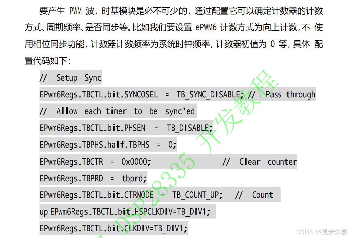
(3)初始化时基模块,即配置 TB 相关寄存器值
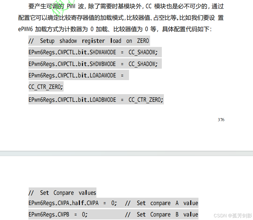
(4)初始化比较模块,即配置 CC 相关寄存器值
(5)初始化动作限定模块,即配置 AQ 相关寄存器值
(6)初始化事件触发模块,即配置 ET 相关寄存器值
当需要事件触发输出控制,就需要对 ET 相关寄存器配置。比如计数器计数 到 0 时,同时使能事件触发中断,每发生一次触发事件就输出 PWM。相关配置代 码如下:
c
EPwm6Regs.ETSEL.bit.INTSEL = ET_CTR_ZERO; // Select INT on Zero event
EPwm6Regs.ETSEL.bit.INTEN = 1; // Enable INT
EPwm6Regs.ETPS.bit.INTPRD = ET_1ST; // Generate INT on 1stevent
(7)初始化死区模块、斩波模块,即配置 DB、PC 相关寄存器值
如果不是特殊应用的话,一般不对死区模块和斩波模块配置,它们的应用方
法在前面各小节也介绍过,所以这里我们不作介绍。
(8)使能时基计数器时钟
将各模块寄存器配置好后,最后开启时基计数器时钟,完成这步操作,对应的IO口即可输出PWM波。开启时基计数器时钟如下:
c
EALLOW;
SysCtrlRegs.PCLKCR0.bit.TBCLKSYNC = 1; // Start all the
timers synced
EDIS;
这里列举的是 ePWM6 的配置,至于其他 ePWM 配置都是一样,只需修改对应
的数字即可。里面涉及到的相关寄存器在前面已做介绍,大家可以用到哪个就查
询哪个,不需要死记硬背。
4 软件设计
4.1 ePWM6 初始化函数
要使用 F28335 的 ePWM6 输出功能,我们必须先对它进行配置。Epwm6 初始化
代码如下:
c
void EPWM6_Init(Uint16 tbprd)
{
EALLOW;
SysCtrlRegs.PCLKCR0.bit.TBCLKSYNC = 0; // Disable TBCLK within
the ePWM
SysCtrlRegs.PCLKCR1.bit.EPWM6ENCLK = 1; // ePWM6
EDIS;
InitEPwm6Gpio();

// Setup Sync
EPwm6Regs.TBCTL.bit.SYNCOSEL = TB_SYNC_DISABLE; // Pass through

// Allow each timer to be sync'ed
EPwm6Regs.TBCTL.bit.PHSEN = TB_DISABLE;
EPwm6Regs.TBPHS.half.TBPHS = 0;
EPwm6Regs.TBCTR = 0x0000; // Clear counter
EPwm6Regs.TBPRD = tbprd;
EPwm6Regs.TBCTL.bit.CTRMODE = TB_COUNT_UP; // Count up
EPwm6Regs.TBCTL.bit.HSPCLKDIV=TB_DIV1;
EPwm6Regs.TBCTL.bit.CLKDIV=TB_DIV1;

// Setup shadow register load on ZERO
EPwm6Regs.CMPCTL.bit.SHDWAMODE = CC_SHADOW;
EPwm6Regs.CMPCTL.bit.SHDWBMODE = CC_SHADOW;
EPwm6Regs.CMPCTL.bit.LOADAMODE = CC_CTR_ZERO;
EPwm6Regs.CMPCTL.bit.LOADBMODE = CC_CTR_ZERO;

// Set Compare values
EPwm6Regs.CMPA.half.CMPA = 0; // Set compare A value
EPwm6Regs.CMPB = 0; // Set Compare B value Zero

// Set actions
EPwm6Regs.AQCTLA.bit.ZRO = AQ_CLEAR; // Set PWM1A on
EPwm6Regs.AQCTLA.bit.CAU = AQ_SET; // Clear PWM1A on event A, up count
EPwm6Regs.AQCTLB.bit.ZRO = AQ_CLEAR; // Set PWM1B on Zero
EPwm6Regs.AQCTLB.bit.CBU = AQ_SET; // Clear PWM1B on event B, up count
EPwm6Regs.ETSEL.bit.INTSEL = ET_CTR_ZERO; // Select INT on Zero event
EPwm6Regs.ETSEL.bit.INTEN = 1; // Enable INT
EPwm6Regs.ETPS.bit.INTPRD = ET_1ST; // Generate INT on 1st event
EALLOW;
SysCtrlRegs.PCLKCR0.bit.TBCLKSYNC = 1; // Start all the
timers synced
EDIS;
}
该函数实现了对 ePWM6 的初始化配置,内部实现过程是按照上一节介绍 ePWM
操作步骤完成,函数的入口带有一个参数 tbprd,通过该参数可修改 ePWM 的频
率。
4.2 主函数
编写好 PWM 初始化函数后,接下来就可以编写主函数了,代码如下:
c
#include "DSP2833x_Device.h" // DSP2833x Headerfile Include File
#include "DSP2833x_Examples.h" // DSP2833x Examples Include File
#include "leds.h" #include "time.h" #include "epwm.h"
/****************************************************************
***************
* 函 数 名 : main
* 函数功能 : 主函数
* 输 入 : 无
* 输 出 : 无
*****************************************************************
**************/
void main()
{
int i=0;
unsigned char fx=0;
InitSysCtrl();
InitPieCtrl();
IER = 0x0000;
IFR = 0x0000;

InitPieVectTable();
// LED_Init();
EPWM6_Init(500);
while(1)
{
if(fx==0)
{
i++;
if(i==300)
{
fx=1;
}
}
else
{
i--;
if(i==0)
{
fx=0;
}
}
 EPwm6A_SetCompare(i); //i 值最大可以取 499,因为 ARR 最大值是 499.
EPwm6B_SetCompare(300-i); //i 值最大可以取 499,因为 ARR 大值是499.
DELAY_US(10*1000);
}
}
主函数实现的功能很简单,首先初始化系统时钟、PIE 中断相关寄存器及中 断
向量表,本套教程所有有关中断代码都采用这种设置,后面就不做重复。再对 使用
到的硬件端口时钟和 IO 口初始化,然后调用我们前面编写的 ePWM6 的初始 化
函数,这里我们设定时基周期寄存器值为 500,计数器计数频率和系统时钟频 率
一致,定时周期即为 3.3us,频率即为 303KHz。最后进入 while 循环语句,
ePWM 开始工作,GPIO10、GPIO11 开始输出 PWM 波形,波形频率约为 303K,你 也
可以修改这个频率值,但是要注意,不能将频率设置过大,否则会看到波形占空比
不明显。通过变量 fx 控制 i 的方向,如果 fx=0,i 值累加, 否则递减,
然后将这个变化的 i 值传递给 EPwm6A_SetCompare 和EPwm6B_SetCompare 函数,
这

5 实验
(1)定时器中断


c
//###########################################################################
//
// FILE:    Example_2833xEPwmTimerInt.c
//
// TITLE:   DSP2833x ePWM Timer Interrupt example.
//
// ASSUMPTIONS:
//
//    This program requires the DSP2833x header files.
//
//    Other then boot mode configuration, no other hardware configuration
//    is required.
//
//    根据在RAM中调试的需要,这个项目配置成"boot to SARAM".2833x引导模式
//    表如下显示. 常用的还有"boot to Flash"模式,当程序在RAM调试完善后就
//    可以将代码烧进Flash中并使用"boot to Flash"引导模式.
//
//       $Boot_Table:
//
//         GPIO87   GPIO86     GPIO85   GPIO84
//          XA15     XA14       XA13     XA12
//           PU       PU         PU       PU
//        ==========================================
//            1        1          1        1    Jump to Flash
//            1        1          1        0    SCI-A boot
//            1        1          0        1    SPI-A boot
//            1        1          0        0    I2C-A boot
//            1        0          1        1    eCAN-A boot
//            1        0          1        0    McBSP-A boot
//            1        0          0        1    Jump to XINTF x16
//            1        0          0        0    Jump to XINTF x32
//            0        1          1        1    Jump to OTP
//            0        1          1        0    Parallel GPIO I/O boot
//            0        1          0        1    Parallel XINTF boot
//            0        1          0        0    Jump to SARAM	    <- "boot to SARAM"
//            0        0          1        1    Branch to check boot mode
//            0        0          1        0    Boot to flash, bypass ADC cal
//            0        0          0        1    Boot to SARAM, bypass ADC cal
//            0        0          0        0    Boot to SCI-A, bypass ADC cal
//                                              Boot_Table_End$
//
// 功能描述
//
//    本例配置ePWM定时器并且每次中断时相应计数变量增加一次
//
//    应用如下:
//
//    所有的ePWM都被初始化.注意28335有6个ePWM,但并不是所有的2833x系列
//    都有6个ePWM
//
//    所有的定时器都有相等的定时周期,所有的定时器同步
//    对于每个ePWM定时器遇到计数0匹配事件时都发生以下响应:
//
//       ePWM1: 每1次0匹配事件发生一次中断
//       ePWM2: 每2次0匹配事件发生一次中断
//       ePWM3: 每3次0匹配事件发生一次中断
//       ePWM4-ePWM6: 每1次0匹配事件发生一次中断
//
//    Thus the Interrupt count for ePWM1, ePWM4-ePWM6 should be equal
//    The interrupt count for ePWM2 should be about half that of ePWM1
//    and the interrupt count for ePWM3 should be about 1/3 that of ePWM1
//
//    Watch Variables:
//       EPwm1TimerIntCount
//       EPwm2TimerIntCount
//       EPwm3TimerIntCount
//       EPwm4TimerIntCount
//       EPwm5TimerIntCount
//       EPwm6TimerIntCount


#include "DSP2833x_Device.h"     // DSP2833x Headerfile Include File
#include "DSP2833x_Examples.h"   // DSP2833x Examples Include File

// Configure which ePWM timer interrupts are enabled at the PIE level:
// 1 = enabled,  0 = disabled
#define PWM1_INT_ENABLE  1
#define PWM2_INT_ENABLE  1
#define PWM3_INT_ENABLE  1
#define PWM4_INT_ENABLE  1
#define PWM5_INT_ENABLE  1
#define PWM6_INT_ENABLE  1

// Configure the period for each timer
#define PWM1_TIMER_TBPRD   0x1FFF
#define PWM2_TIMER_TBPRD   0x1FFF
#define PWM3_TIMER_TBPRD   0x1FFF
#define PWM4_TIMER_TBPRD   0x1FFF
#define PWM5_TIMER_TBPRD   0x1FFF
#define PWM6_TIMER_TBPRD   0x1FFF


// Prototype statements for functions found within this file.
interrupt void epwm1_timer_isr(void);
interrupt void epwm2_timer_isr(void);
interrupt void epwm3_timer_isr(void);
interrupt void epwm4_timer_isr(void);
interrupt void epwm5_timer_isr(void);
interrupt void epwm6_timer_isr(void);
void InitEPwmTimer(void);

// Global variables used in this example
Uint32  EPwm1TimerIntCount;
Uint32  EPwm2TimerIntCount;
Uint32  EPwm3TimerIntCount;
Uint32  EPwm4TimerIntCount;
Uint32  EPwm5TimerIntCount;
Uint32  EPwm6TimerIntCount;


void main(void)
{
   int i;

// Step 1. Initialize System Control:
// PLL, WatchDog, enable Peripheral Clocks
// This example function is found in the DSP2833x_SysCtrl.c file.
   InitSysCtrl();

// Step 2. Initalize GPIO:
// This example function is found in the DSP2833x_Gpio.c file and
// illustrates how to set the GPIO to it's default state.
// InitGpio();  // Skipped for this example


// Step 3. Clear all interrupts and initialize PIE vector table:
// Disable CPU interrupts
   DINT;

// Initialize the PIE control registers to their default state.
// The default state is all PIE interrupts disabled and flags
// are cleared.
// This function is found in the DSP2833x_PieCtrl.c file.
   InitPieCtrl();

// Disable CPU interrupts and clear all CPU interrupt flags:
   IER = 0x0000;
   IFR = 0x0000;

// Initialize the PIE vector table with pointers to the shell Interrupt
// Service Routines (ISR).
// This will populate the entire table, even if the interrupt
// is not used in this example.  This is useful for debug purposes.
// The shell ISR routines are found in DSP2833x_DefaultIsr.c.
// This function is found in DSP2833x_PieVect.c.
   InitPieVectTable();

// Interrupts that are used in this example are re-mapped to
// ISR functions found within this file.
   EALLOW;  // This is needed to write to EALLOW protected registers
   PieVectTable.EPWM1_INT = &epwm1_timer_isr;
   PieVectTable.EPWM2_INT = &epwm2_timer_isr;
   PieVectTable.EPWM3_INT = &epwm3_timer_isr;
   PieVectTable.EPWM4_INT = &epwm4_timer_isr;
   PieVectTable.EPWM5_INT = &epwm5_timer_isr;
   PieVectTable.EPWM6_INT = &epwm6_timer_isr;
   EDIS;    // This is needed to disable write to EALLOW protected registers

// Step 4. Initialize all the Device Peripherals:
// This function is found in DSP2833x_InitPeripherals.c
// InitPeripherals();  // Not required for this example
   InitEPwmTimer();    // For this example, only initialize the ePWM Timers

// Step 5. User specific code, enable interrupts:

// Initalize counters:
   EPwm1TimerIntCount = 0;
   EPwm2TimerIntCount = 0;
   EPwm3TimerIntCount = 0;
   EPwm4TimerIntCount = 0;
   EPwm5TimerIntCount = 0;
   EPwm6TimerIntCount = 0;

// Enable CPU INT3 which is connected to EPWM1-6 INT:
   IER |= M_INT3;

// Enable EPWM INTn in the PIE: Group 3 interrupt 1-6
   PieCtrlRegs.PIEIER3.bit.INTx1 = PWM1_INT_ENABLE;
   PieCtrlRegs.PIEIER3.bit.INTx2 = PWM2_INT_ENABLE;
   PieCtrlRegs.PIEIER3.bit.INTx3 = PWM3_INT_ENABLE;
   PieCtrlRegs.PIEIER3.bit.INTx4 = PWM4_INT_ENABLE;
   PieCtrlRegs.PIEIER3.bit.INTx5 = PWM5_INT_ENABLE;
   PieCtrlRegs.PIEIER3.bit.INTx6 = PWM6_INT_ENABLE;

// Enable global Interrupts and higher priority real-time debug events:
   EINT;   // Enable Global interrupt INTM
   ERTM;   // Enable Global realtime interrupt DBGM

// Step 6. IDLE loop. Just sit and loop forever (optional):
   for(;;)
   {
       asm("          NOP");
       for(i=1;i<=10;i++)
       {}
   }

}


void InitEPwmTimer()
{

   EALLOW;
   SysCtrlRegs.PCLKCR0.bit.TBCLKSYNC = 0;      // Stop all the TB clocks
   EDIS;

   // Setup Sync
   EPwm1Regs.TBCTL.bit.SYNCOSEL = TB_SYNC_IN;  // Pass through
   EPwm2Regs.TBCTL.bit.SYNCOSEL = TB_SYNC_IN;  // Pass through
   EPwm3Regs.TBCTL.bit.SYNCOSEL = TB_SYNC_IN;  // Pass through
   EPwm4Regs.TBCTL.bit.SYNCOSEL = TB_SYNC_IN;  // Pass through
   EPwm5Regs.TBCTL.bit.SYNCOSEL = TB_SYNC_IN;  // Pass through
   EPwm6Regs.TBCTL.bit.SYNCOSEL = TB_SYNC_IN;  // Pass through

   // Allow each timer to be sync'ed

   EPwm1Regs.TBCTL.bit.PHSEN = TB_ENABLE;
   EPwm2Regs.TBCTL.bit.PHSEN = TB_ENABLE;
   EPwm3Regs.TBCTL.bit.PHSEN = TB_ENABLE;
   EPwm4Regs.TBCTL.bit.PHSEN = TB_ENABLE;
   EPwm5Regs.TBCTL.bit.PHSEN = TB_ENABLE;
   EPwm6Regs.TBCTL.bit.PHSEN = TB_ENABLE;

   EPwm1Regs.TBPHS.half.TBPHS = 100;
   EPwm2Regs.TBPHS.half.TBPHS = 200;
   EPwm3Regs.TBPHS.half.TBPHS = 300;
   EPwm4Regs.TBPHS.half.TBPHS = 400;
   EPwm5Regs.TBPHS.half.TBPHS = 500;
   EPwm6Regs.TBPHS.half.TBPHS = 600;

   EPwm1Regs.TBPRD = PWM1_TIMER_TBPRD;
   EPwm1Regs.TBCTL.bit.CTRMODE = TB_COUNT_UP;    // Count up
   EPwm1Regs.ETSEL.bit.INTSEL = ET_CTR_ZERO;     // Select INT on Zero event
   EPwm1Regs.ETSEL.bit.INTEN = PWM1_INT_ENABLE;  // Enable INT
   EPwm1Regs.ETPS.bit.INTPRD = ET_1ST;           // Generate INT on 1st event


   EPwm2Regs.TBPRD = PWM2_TIMER_TBPRD;
   EPwm2Regs.TBCTL.bit.CTRMODE = TB_COUNT_UP;     // Count up
   EPwm2Regs.ETSEL.bit.INTSEL = ET_CTR_ZERO;      // Enable INT on Zero event
   EPwm2Regs.ETSEL.bit.INTEN = PWM2_INT_ENABLE;   // Enable INT
   EPwm2Regs.ETPS.bit.INTPRD = ET_2ND;            // Generate INT on 2nd event


   EPwm3Regs.TBPRD = PWM3_TIMER_TBPRD;
   EPwm3Regs.TBCTL.bit.CTRMODE = TB_COUNT_UP;     // Count up
   EPwm3Regs.ETSEL.bit.INTSEL = ET_CTR_ZERO;      // Enable INT on Zero event
   EPwm3Regs.ETSEL.bit.INTEN = PWM3_INT_ENABLE;   // Enable INT
   EPwm3Regs.ETPS.bit.INTPRD = ET_3RD;            // Generate INT on 3rd event

   EPwm4Regs.TBPRD = PWM4_TIMER_TBPRD;
   EPwm4Regs.TBCTL.bit.CTRMODE = TB_COUNT_UP;     // Count up
   EPwm4Regs.ETSEL.bit.INTSEL = ET_CTR_ZERO;      // Enable INT on Zero event
   EPwm4Regs.ETSEL.bit.INTEN = PWM4_INT_ENABLE;   // Enable INT
   EPwm4Regs.ETPS.bit.INTPRD = ET_1ST;            // Generate INT on 1st event


   EPwm5Regs.TBPRD = PWM5_TIMER_TBPRD;
   EPwm5Regs.TBCTL.bit.CTRMODE= TB_COUNT_UP;      // Count up
   EPwm5Regs.ETSEL.bit.INTSEL = ET_CTR_ZERO;      // Enable INT on Zero event
   EPwm5Regs.ETSEL.bit.INTEN = PWM5_INT_ENABLE;   // Enable INT
   EPwm5Regs.ETPS.bit.INTPRD = ET_1ST;            // Generate INT on 1st event


   EPwm6Regs.TBPRD = PWM6_TIMER_TBPRD;
   EPwm6Regs.TBCTL.bit.CTRMODE = TB_COUNT_UP;     // Count up
   EPwm6Regs.ETSEL.bit.INTSEL = ET_CTR_ZERO;      // Enable INT on Zero event
   EPwm6Regs.ETSEL.bit.INTEN = PWM6_INT_ENABLE;   // Enable INT
   EPwm6Regs.ETPS.bit.INTPRD = ET_1ST;            // Generate INT on 1st event

   EALLOW;
   SysCtrlRegs.PCLKCR0.bit.TBCLKSYNC = 1;         // Start all the timers synced
   EDIS;


}


// Interrupt routines uses in this example:
interrupt void epwm1_timer_isr(void)
{
   EPwm1TimerIntCount++;

   // Clear INT flag for this timer
   EPwm1Regs.ETCLR.bit.INT = 1;

   // Acknowledge this interrupt to receive more interrupts from group 3
   PieCtrlRegs.PIEACK.all = PIEACK_GROUP3;
}

interrupt void epwm2_timer_isr(void)
{
   EPwm2TimerIntCount++;

   // Clear INT flag for this timer
   EPwm2Regs.ETCLR.bit.INT = 1;

   // Acknowledge this interrupt to receive more interrupts from group 3
   PieCtrlRegs.PIEACK.all = PIEACK_GROUP3;
}

interrupt void epwm3_timer_isr(void)
{
   EPwm3TimerIntCount++;

   // Clear INT flag for this timer
   EPwm3Regs.ETCLR.bit.INT = 1;

   // Acknowledge this interrupt to receive more interrupts from group 3
   PieCtrlRegs.PIEACK.all = PIEACK_GROUP3;
}

interrupt void epwm4_timer_isr(void)
{
   EPwm4TimerIntCount++;

   // Clear INT flag for this timer
   EPwm4Regs.ETCLR.bit.INT = 1;

   // Acknowledge this interrupt to receive more interrupts from group 3
   PieCtrlRegs.PIEACK.all = PIEACK_GROUP3;
}

interrupt void epwm5_timer_isr(void)
{
   EPwm5TimerIntCount++;

   // Clear INT flag for this timer
   EPwm5Regs.ETCLR.bit.INT = 1;

   // Acknowledge this interrupt to receive more interrupts from group 3
   PieCtrlRegs.PIEACK.all = PIEACK_GROUP3;
}

interrupt void epwm6_timer_isr(void)
{
   EPwm6TimerIntCount++;

   // Clear INT flag for this timer
   EPwm6Regs.ETCLR.bit.INT = 1;

   // Acknowledge this interrupt to receive more interrupts from group 3
   PieCtrlRegs.PIEACK.all = PIEACK_GROUP3;
}


//===========================================================================
// No more.
//===========================================================================
(2)动作限定模块增计数占空比模式


c
//###########################################################################
//
// 文件:    Example_2833xEPwm3UpAQ.c
//
// 标题:   动作限定模块增计数模式
//
// ASSUMPTIONS:
//
//     此程序需要 DSP2833x头文件.
//
//     按以下描述用示波器观察 ePWM1 - ePWM3引脚
//
//        EPWM1A定义在GPIO0上
//        EPWM1B定义在GPIO1上
//
//        EPWM2A定义在GPIO2上
//        EPWM2B定义在GPIO3上
//
//        EPWM3A定义在GPIO4上
//        EPWM3B定义在GPIO5上
//
//    根据在RAM中调试的需要,这个项目配置成"boot to SARAM".2833x引导模式
//    表如下显示. 常用的还有"boot to Flash"模式,当程序在RAM调试完善后就
//    可以将代码烧进Flash中并使用"boot to Flash"引导模式.
//
//       $Boot_Table:
//
//         GPIO87   GPIO86     GPIO85   GPIO84
//          XA15     XA14       XA13     XA12
//           PU       PU         PU       PU
//        ==========================================
//            1        1          1        1    Jump to Flash
//            1        1          1        0    SCI-A boot
//            1        1          0        1    SPI-A boot
//            1        1          0        0    I2C-A boot
//            1        0          1        1    eCAN-A boot
//            1        0          1        0    McBSP-A boot
//            1        0          0        1    Jump to XINTF x16
//            1        0          0        0    Jump to XINTF x32
//            0        1          1        1    Jump to OTP
//            0        1          1        0    Parallel GPIO I/O boot
//            0        1          0        1    Parallel XINTF boot
//            0        1          0        0    Jump to SARAM	    <- "boot to SARAM"
//            0        0          1        1    Branch to check boot mode
//            0        0          1        0    Boot to flash, bypass ADC cal
//            0        0          0        1    Boot to SARAM, bypass ADC cal
//            0        0          0        0    Boot to SCI-A, bypass ADC cal
//                                              Boot_Table_End$
//
// 描述:
//
//    本例配置ePWM1, ePWM2, ePWM3产生产生EPWMxA和EPWMxB波形
//
//    在ePWM中断子程序中,比较寄存器CMPA和CMPB的值被修改
//
//    本例时基时钟被配置为增计数模式
//    通过示波器观察EPWM1A/B, EPWM2A/B 和 EPWM3A/B波形
//
//###########################################################################
// 释放日期:2013.11.26
//###########################################################################


#include "DSP2833x_Device.h"     // DSP2833x Headerfile Include File
#include "DSP2833x_Examples.h"   // DSP2833x Examples Include File


typedef struct
{
   volatile struct EPWM_REGS *EPwmRegHandle;
   Uint16 EPwm_CMPA_Direction;
   Uint16 EPwm_CMPB_Direction;
   Uint16 EPwmTimerIntCount;
   Uint16 EPwmMaxCMPA;
   Uint16 EPwmMinCMPA;
   Uint16 EPwmMaxCMPB;
   Uint16 EPwmMinCMPB;
}EPWM_INFO;


// Prototype statements for functions found within this file.
void InitEPwm1Example(void);
void InitEPwm2Example(void);
void InitEPwm3Example(void);
interrupt void epwm1_isr(void);
interrupt void epwm2_isr(void);
interrupt void epwm3_isr(void);
void update_compare(EPWM_INFO*);

// Global variables used in this example
EPWM_INFO epwm1_info;
EPWM_INFO epwm2_info;
EPWM_INFO epwm3_info;

// Configure the period for each timer
#define EPWM1_TIMER_TBPRD  2000  // Period register
#define EPWM1_MAX_CMPA     1950
#define EPWM1_MIN_CMPA       50
#define EPWM1_MAX_CMPB     1950
#define EPWM1_MIN_CMPB       50

#define EPWM2_TIMER_TBPRD  2000  // Period register
#define EPWM2_MAX_CMPA     1950
#define EPWM2_MIN_CMPA       50
#define EPWM2_MAX_CMPB     1950
#define EPWM2_MIN_CMPB       50

#define EPWM3_TIMER_TBPRD  2000  // Period register
#define EPWM3_MAX_CMPA      950
#define EPWM3_MIN_CMPA       50
#define EPWM3_MAX_CMPB     1950
#define EPWM3_MIN_CMPB     1050


// To keep track of which way the compare value is moving
#define EPWM_CMP_UP   1
#define EPWM_CMP_DOWN 0


void main(void)
{
// Step 1. Initialize System Control:
// PLL, WatchDog, enable Peripheral Clocks
// This example function is found in the DSP2833x_SysCtrl.c file.
   InitSysCtrl();

// Step 2. Initalize GPIO:
// This example function is found in the DSP2833x_Gpio.c file and
// illustrates how to set the GPIO to it's default state.
// InitGpio();  // Skipped for this example

// For this case just init GPIO pins for ePWM1, ePWM2, ePWM3
// These functions are in the DSP2833x_EPwm.c file
   InitEPwm1Gpio();
   InitEPwm2Gpio();
   InitEPwm3Gpio();


// Step 3. Clear all interrupts and initialize PIE vector table:
// Disable CPU interrupts
   DINT;

// Initialize the PIE control registers to their default state.
// The default state is all PIE interrupts disabled and flags
// are cleared.
// This function is found in the DSP2833x_PieCtrl.c file.
   InitPieCtrl();

// Disable CPU interrupts and clear all CPU interrupt flags:
   IER = 0x0000;
   IFR = 0x0000;

// Initialize the PIE vector table with pointers to the shell Interrupt
// Service Routines (ISR).
// This will populate the entire table, even if the interrupt
// is not used in this example.  This is useful for debug purposes.
// The shell ISR routines are found in DSP2833x_DefaultIsr.c.
// This function is found in DSP2833x_PieVect.c.
   InitPieVectTable();

// Interrupts that are used in this example are re-mapped to
// ISR functions found within this file.
   EALLOW;  // This is needed to write to EALLOW protected registers
   PieVectTable.EPWM1_INT = &epwm1_isr;
   PieVectTable.EPWM2_INT = &epwm2_isr;
   PieVectTable.EPWM3_INT = &epwm3_isr;
   EDIS;    // This is needed to disable write to EALLOW protected registers

// Step 4. Initialize all the Device Peripherals:
// This function is found in DSP2833x_InitPeripherals.c
// InitPeripherals();  // Not required for this example

// For this example, only initialize the ePWM

   EALLOW;
   SysCtrlRegs.PCLKCR0.bit.TBCLKSYNC = 0;
   EDIS;

   InitEPwm1Example();
   InitEPwm2Example();
   InitEPwm3Example();

   EALLOW;
   SysCtrlRegs.PCLKCR0.bit.TBCLKSYNC = 1;
   EDIS;


// Step 5. User specific code, enable interrupts:

// Enable CPU INT3 which is connected to EPWM1-3 INT:
   IER |= M_INT3;

// Enable EPWM INTn in the PIE: Group 3 interrupt 1-3
   PieCtrlRegs.PIEIER3.bit.INTx1 = 1;
   PieCtrlRegs.PIEIER3.bit.INTx2 = 1;
   PieCtrlRegs.PIEIER3.bit.INTx3 = 1;

// Enable global Interrupts and higher priority real-time debug events:
   EINT;   // Enable Global interrupt INTM
   ERTM;   // Enable Global realtime interrupt DBGM

// Step 6. IDLE loop. Just sit and loop forever (optional):
   for(;;)
   {
       asm("          NOP");
   }

}

interrupt void epwm1_isr(void)
{
   // Update the CMPA and CMPB values
   update_compare(&epwm1_info);

   // Clear INT flag for this timer
   EPwm1Regs.ETCLR.bit.INT = 1;

   // Acknowledge this interrupt to receive more interrupts from group 3
   PieCtrlRegs.PIEACK.all = PIEACK_GROUP3;
}


interrupt void epwm2_isr(void)
{

   // Update the CMPA and CMPB values
   update_compare(&epwm2_info);

   // Clear INT flag for this timer
   EPwm2Regs.ETCLR.bit.INT = 1;

   // Acknowledge this interrupt to receive more interrupts from group 3
   PieCtrlRegs.PIEACK.all = PIEACK_GROUP3;
}

interrupt void epwm3_isr(void)
{

   // Update the CMPA and CMPB values
   update_compare(&epwm3_info);

   // Clear INT flag for this timer
   EPwm3Regs.ETCLR.bit.INT = 1;

   // Acknowledge this interrupt to receive more interrupts from group 3
   PieCtrlRegs.PIEACK.all = PIEACK_GROUP3;
}

void InitEPwm1Example()
{

   // Setup TBCLK
   EPwm1Regs.TBCTL.bit.CTRMODE = TB_COUNT_UP; // Count up
   EPwm1Regs.TBPRD = EPWM1_TIMER_TBPRD;       // Set timer period
   EPwm1Regs.TBCTL.bit.PHSEN = TB_DISABLE;    // Disable phase loading
   EPwm1Regs.TBPHS.half.TBPHS = 0x0000;       // Phase is 0
   EPwm1Regs.TBCTR = 0x0000;                  // Clear counter
   EPwm1Regs.TBCTL.bit.HSPCLKDIV = TB_DIV2;   // Clock ratio to SYSCLKOUT
   EPwm1Regs.TBCTL.bit.CLKDIV = TB_DIV2;

   // Setup shadow register load on ZERO
   EPwm1Regs.CMPCTL.bit.SHDWAMODE = CC_SHADOW;
   EPwm1Regs.CMPCTL.bit.SHDWBMODE = CC_SHADOW;
   EPwm1Regs.CMPCTL.bit.LOADAMODE = CC_CTR_ZERO;
   EPwm1Regs.CMPCTL.bit.LOADBMODE = CC_CTR_ZERO;

   // Set Compare values
   EPwm1Regs.CMPA.half.CMPA = EPWM1_MIN_CMPA;    // Set compare A value
   EPwm1Regs.CMPB = EPWM1_MIN_CMPB;              // Set Compare B value

   // Set actions
   EPwm1Regs.AQCTLA.bit.ZRO = AQ_SET;            // Set PWM1A on Zero
   EPwm1Regs.AQCTLA.bit.CAU = AQ_CLEAR;          // Clear PWM1A on event A, upcount

   EPwm1Regs.AQCTLB.bit.ZRO = AQ_SET;            // Set PWM1B on Zero
   EPwm1Regs.AQCTLB.bit.CBU = AQ_CLEAR;          // Clear PWM1B on event B, upcount

   // Interrupt where we will change the Compare Values
   EPwm1Regs.ETSEL.bit.INTSEL = ET_CTR_ZERO;     // Select INT on Zero event
   EPwm1Regs.ETSEL.bit.INTEN = 1;                // Enable INT
   EPwm1Regs.ETPS.bit.INTPRD = ET_3RD;           // Generate INT on 3rd event

   // Information this example uses to keep track
   // of the direction the CMPA/CMPB values are
   // moving, the min and max allowed values and
   // a pointer to the correct ePWM registers
   epwm1_info.EPwm_CMPA_Direction = EPWM_CMP_UP; // Start by increasing CMPA & CMPB
   epwm1_info.EPwm_CMPB_Direction = EPWM_CMP_UP;
   epwm1_info.EPwmTimerIntCount = 0;             // Zero the interrupt counter
   epwm1_info.EPwmRegHandle = &EPwm1Regs;        // Set the pointer to the ePWM module
   epwm1_info.EPwmMaxCMPA = EPWM1_MAX_CMPA;      // Setup min/max CMPA/CMPB values
   epwm1_info.EPwmMinCMPA = EPWM1_MIN_CMPA;
   epwm1_info.EPwmMaxCMPB = EPWM1_MAX_CMPB;
   epwm1_info.EPwmMinCMPB = EPWM1_MIN_CMPB;

}


void InitEPwm2Example()
{
   // Setup TBCLK
   EPwm2Regs.TBCTL.bit.CTRMODE = TB_COUNT_UP; // Count up
   EPwm2Regs.TBPRD = EPWM2_TIMER_TBPRD;       // Set timer period
   EPwm2Regs.TBCTL.bit.PHSEN = TB_DISABLE;    // Disable phase loading
   EPwm2Regs.TBPHS.half.TBPHS = 0x0000;       // Phase is 0
   EPwm2Regs.TBCTR = 0x0000;                  // Clear counter
   EPwm2Regs.TBCTL.bit.HSPCLKDIV = TB_DIV2;   // Clock ratio to SYSCLKOUT
   EPwm2Regs.TBCTL.bit.CLKDIV = TB_DIV2;

   // Setup shadow register load on ZERO
   EPwm2Regs.CMPCTL.bit.SHDWAMODE = CC_SHADOW;
   EPwm2Regs.CMPCTL.bit.SHDWBMODE = CC_SHADOW;
   EPwm2Regs.CMPCTL.bit.LOADAMODE = CC_CTR_ZERO;
   EPwm2Regs.CMPCTL.bit.LOADBMODE = CC_CTR_ZERO;

   // Set Compare values
   EPwm2Regs.CMPA.half.CMPA = EPWM2_MIN_CMPA;       // Set compare A value
   EPwm2Regs.CMPB = EPWM2_MAX_CMPB;                 // Set Compare B value

   // Set actions
   EPwm2Regs.AQCTLA.bit.PRD = AQ_CLEAR;             // Clear PWM2A on Period
   EPwm2Regs.AQCTLA.bit.CAU = AQ_SET;               // Set PWM2A on event A, up count

   EPwm2Regs.AQCTLB.bit.PRD = AQ_CLEAR;             // Clear PWM2B on Period
   EPwm2Regs.AQCTLB.bit.CBU = AQ_SET;               // Set PWM2B on event B, up count

   // Interrupt where we will change the Compare Values
   EPwm2Regs.ETSEL.bit.INTSEL = ET_CTR_ZERO;        // Select INT on Zero event
   EPwm2Regs.ETSEL.bit.INTEN = 1;                   // Enable INT
   EPwm2Regs.ETPS.bit.INTPRD = ET_3RD;              // Generate INT on 3rd event

   // Information this example uses to keep track
   // of the direction the CMPA/CMPB values are
   // moving, the min and max allowed values and
   // a pointer to the correct ePWM registers
   epwm2_info.EPwm_CMPA_Direction = EPWM_CMP_UP;    // Start by increasing CMPA
   epwm2_info.EPwm_CMPB_Direction = EPWM_CMP_DOWN;  // and decreasing CMPB
   epwm2_info.EPwmTimerIntCount = 0;                // Zero the interrupt counter
   epwm2_info.EPwmRegHandle = &EPwm2Regs;           // Set the pointer to the ePWM module
   epwm2_info.EPwmMaxCMPA = EPWM2_MAX_CMPA;         // Setup min/max CMPA/CMPB values
   epwm2_info.EPwmMinCMPA = EPWM2_MIN_CMPA;
   epwm2_info.EPwmMaxCMPB = EPWM2_MAX_CMPB;
   epwm2_info.EPwmMinCMPB = EPWM2_MIN_CMPB;

}


void InitEPwm3Example(void)
{


   // Setup TBCLK
   EPwm3Regs.TBCTL.bit.CTRMODE = TB_COUNT_UP; // Count up
   EPwm3Regs.TBPRD = EPWM3_TIMER_TBPRD;       // Set timer period
   EPwm3Regs.TBCTL.bit.PHSEN = TB_DISABLE;    // Disable phase loading
   EPwm3Regs.TBPHS.half.TBPHS = 0x0000;       // Phase is 0
   EPwm3Regs.TBCTR = 0x0000;                  // Clear counter
   EPwm3Regs.TBCTL.bit.HSPCLKDIV = TB_DIV1;   // Clock ratio to SYSCLKOUT
   EPwm3Regs.TBCTL.bit.CLKDIV = TB_DIV1;

   // Setup shadow register load on ZERO
   EPwm3Regs.CMPCTL.bit.SHDWAMODE = CC_SHADOW;
   EPwm3Regs.CMPCTL.bit.SHDWBMODE = CC_SHADOW;
   EPwm3Regs.CMPCTL.bit.LOADAMODE = CC_CTR_ZERO;
   EPwm3Regs.CMPCTL.bit.LOADBMODE = CC_CTR_ZERO;

  // Set Compare values
   EPwm3Regs.CMPA.half.CMPA = EPWM3_MIN_CMPA; // Set compare A value
   EPwm3Regs.CMPB = EPWM3_MAX_CMPB;           // Set Compare B value

   // Set Actions
   EPwm3Regs.AQCTLA.bit.CAU = AQ_SET;         // Set PWM3A on event B, up count
   EPwm3Regs.AQCTLA.bit.CBU = AQ_CLEAR;       // Clear PWM3A on event B, up count

   EPwm3Regs.AQCTLB.bit.ZRO = AQ_TOGGLE;      // Toggle EPWM3B on Zero

   // Interrupt where we will change the Compare Values
   EPwm3Regs.ETSEL.bit.INTSEL = ET_CTR_ZERO;     // Select INT on Zero event
   EPwm3Regs.ETSEL.bit.INTEN = 1;                // Enable INT
   EPwm3Regs.ETPS.bit.INTPRD = ET_3RD;           // Generate INT on 3rd event

   // Start by increasing the compare A and decreasing compare B
   epwm3_info.EPwm_CMPA_Direction = EPWM_CMP_UP;
   epwm3_info.EPwm_CMPB_Direction = EPWM_CMP_DOWN;
   // Start the cout at 0
   epwm3_info.EPwmTimerIntCount = 0;
   epwm3_info.EPwmRegHandle = &EPwm3Regs;
   epwm3_info.EPwmMaxCMPA = EPWM3_MAX_CMPA;
   epwm3_info.EPwmMinCMPA = EPWM3_MIN_CMPA;
   epwm3_info.EPwmMaxCMPB = EPWM3_MAX_CMPB;
   epwm3_info.EPwmMinCMPB = EPWM3_MIN_CMPB;
}


void update_compare(EPWM_INFO *epwm_info)
{


   // Every 10'th interrupt, change the CMPA/CMPB values
   if(epwm_info->EPwmTimerIntCount == 10)
   {
       epwm_info->EPwmTimerIntCount = 0;

       // If we were increasing CMPA, check to see if
       // we reached the max value.  If not, increase CMPA
       // else, change directions and decrease CMPA
	   if(epwm_info->EPwm_CMPA_Direction == EPWM_CMP_UP)
	   {
	       if(epwm_info->EPwmRegHandle->CMPA.half.CMPA < epwm_info->EPwmMaxCMPA)
	       {
	          epwm_info->EPwmRegHandle->CMPA.half.CMPA++;
	       }
	       else
	       {
	          epwm_info->EPwm_CMPA_Direction = EPWM_CMP_DOWN;
              epwm_info->EPwmRegHandle->CMPA.half.CMPA--;
	       }
	   }

	   // If we were decreasing CMPA, check to see if
       // we reached the min value.  If not, decrease CMPA
       // else, change directions and increase CMPA
	   else
	   {
	       if(epwm_info->EPwmRegHandle->CMPA.half.CMPA == epwm_info->EPwmMinCMPA)
	       {
	          epwm_info->EPwm_CMPA_Direction = EPWM_CMP_UP;
	          epwm_info->EPwmRegHandle->CMPA.half.CMPA++;
	       }
	       else
	       {
	          epwm_info->EPwmRegHandle->CMPA.half.CMPA--;
	       }
	   }

	   // If we were increasing CMPB, check to see if
       // we reached the max value.  If not, increase CMPB
       // else, change directions and decrease CMPB
	   if(epwm_info->EPwm_CMPB_Direction == EPWM_CMP_UP)
	   {
	       if(epwm_info->EPwmRegHandle->CMPB < epwm_info->EPwmMaxCMPB)
	       {
	          epwm_info->EPwmRegHandle->CMPB++;
	       }
	       else
	       {
	          epwm_info->EPwm_CMPB_Direction = EPWM_CMP_DOWN;
	          epwm_info->EPwmRegHandle->CMPB--;
	       }
	   }

	   // If we were decreasing CMPB, check to see if
       // we reached the min value.  If not, decrease CMPB
       // else, change directions and increase CMPB

	   else
	   {
	       if(epwm_info->EPwmRegHandle->CMPB == epwm_info->EPwmMinCMPB)
	       {
	          epwm_info->EPwm_CMPB_Direction = EPWM_CMP_UP;
	          epwm_info->EPwmRegHandle->CMPB++;
	       }
	       else
	       {
	          epwm_info->EPwmRegHandle->CMPB--;
	       }
	   }
   }
   else
   {
      epwm_info->EPwmTimerIntCount++;
   }

   return;
}


//===========================================================================
// No more.
//===========================================================================
(3)动作限定模块 - 使用增/减计数模式


c
//###########################################################################
//
// 文件名:    Example_2833xEPwmUpDownAQ.c
//
// 标题:   动作限定模块 - 使用增/减计数模式
//
//
//     此程序需要 DSP2833x头文件.
//
//     按以下描述用示波器观察 ePWM1 - ePWM3引脚
//
//        EPWM1A定义在GPIO0上
//        EPWM1B定义在GPIO1上
//
//        EPWM2A定义在GPIO2上
//        EPWM2B定义在GPIO3上
//
//        EPWM3A定义在GPIO4上
//        EPWM3B定义在GPIO5上
//
//    根据在RAM中调试的需要,这个项目配置成"boot to SARAM".2833x引导模式
//    表如下显示. 常用的还有"boot to Flash"模式,当程序在RAM调试完善后就
//    可以将代码烧进Flash中并使用"boot to Flash"引导模式.
//
//       $Boot_Table:
//
//         GPIO87   GPIO86     GPIO85   GPIO84
//          XA15     XA14       XA13     XA12
//           PU       PU         PU       PU
//        ==========================================
//            1        1          1        1    Jump to Flash
//            1        1          1        0    SCI-A boot
//            1        1          0        1    SPI-A boot
//            1        1          0        0    I2C-A boot
//            1        0          1        1    eCAN-A boot
//            1        0          1        0    McBSP-A boot
//            1        0          0        1    Jump to XINTF x16
//            1        0          0        0    Jump to XINTF x32
//            0        1          1        1    Jump to OTP
//            0        1          1        0    Parallel GPIO I/O boot
//            0        1          0        1    Parallel XINTF boot
//            0        1          0        0    Jump to SARAM	    <- "boot to SARAM"
//            0        0          1        1    Branch to check boot mode
//            0        0          1        0    Boot to flash, bypass ADC cal
//            0        0          0        1    Boot to SARAM, bypass ADC cal
//            0        0          0        0    Boot to SCI-A, bypass ADC cal
//                                              Boot_Table_End$
//
// 功能描述:
//
//     本例配置ePWM1, ePWM2, ePWM3产生产生EPWMxA和EPWMxB波形
//
//    在ePWM中断子程序中,比较寄存器CMPA和CMPB的值被修改
//
//    本例时基时钟被配置为增减计数模式
//    通过示波器观察EPWM1A/B, EPWM2A/B 和 EPWM3A/B波形
//
//
//###########################################################################
// 释放日期:2013.11.25
//###########################################################################


#include "DSP2833x_Device.h"     // DSP2833x Headerfile Include File
#include "DSP2833x_Examples.h"   // DSP2833x Examples Include File

typedef struct
{
   volatile struct EPWM_REGS *EPwmRegHandle;
   Uint16 EPwm_CMPA_Direction;
   Uint16 EPwm_CMPB_Direction;
   Uint16 EPwmTimerIntCount;
   Uint16 EPwmMaxCMPA;
   Uint16 EPwmMinCMPA;
   Uint16 EPwmMaxCMPB;
   Uint16 EPwmMinCMPB;
}EPWM_INFO;


// Prototype statements for functions found within this file.
void InitEPwm1Example(void);
void InitEPwm2Example(void);
void InitEPwm3Example(void);
interrupt void epwm1_isr(void);
interrupt void epwm2_isr(void);
interrupt void epwm3_isr(void);
void update_compare(EPWM_INFO*);

// Global variables used in this example
EPWM_INFO epwm1_info;
EPWM_INFO epwm2_info;
EPWM_INFO epwm3_info;

// Configure the period for each timer
#define EPWM1_TIMER_TBPRD  2000  // Period register
#define EPWM1_MAX_CMPA     1950
#define EPWM1_MIN_CMPA       50
#define EPWM1_MAX_CMPB     1950
#define EPWM1_MIN_CMPB       50

#define EPWM2_TIMER_TBPRD  2000  // Period register
#define EPWM2_MAX_CMPA     1950
#define EPWM2_MIN_CMPA       50
#define EPWM2_MAX_CMPB     1950
#define EPWM2_MIN_CMPB       50

#define EPWM3_TIMER_TBPRD  2000  // Period register
#define EPWM3_MAX_CMPA      950
#define EPWM3_MIN_CMPA       50
#define EPWM3_MAX_CMPB     1950
#define EPWM3_MIN_CMPB     1050

// To keep track of which way the compare value is moving
#define EPWM_CMP_UP   1
#define EPWM_CMP_DOWN 0

void main(void)
{
// Step 1. Initialize System Control:
// PLL, WatchDog, enable Peripheral Clocks
// This example function is found in the DSP2833x_SysCtrl.c file.
   InitSysCtrl();

// Step 2. Initalize GPIO:
// This example function is found in the DSP2833x_Gpio.c file and
// illustrates how to set the GPIO to it's default state.
// InitGpio();  // Skipped for this example

// For this case just init GPIO pins for ePWM1, ePWM2, ePWM3
// These functions are in the DSP2833x_EPwm.c file
   InitEPwm1Gpio();
   InitEPwm2Gpio();
   InitEPwm3Gpio();

// Step 3. Clear all interrupts and initialize PIE vector table:
// Disable CPU interrupts
   DINT;

// Initialize the PIE control registers to their default state.
// The default state is all PIE interrupts disabled and flags
// are cleared.
// This function is found in the DSP2833x_PieCtrl.c file.
   InitPieCtrl();

// Disable CPU interrupts and clear all CPU interrupt flags:
   IER = 0x0000;
   IFR = 0x0000;

// Initialize the PIE vector table with pointers to the shell Interrupt
// Service Routines (ISR).
// This will populate the entire table, even if the interrupt
// is not used in this example.  This is useful for debug purposes.
// The shell ISR routines are found in DSP2833x_DefaultIsr.c.
// This function is found in DSP2833x_PieVect.c.
   InitPieVectTable();

// Interrupts that are used in this example are re-mapped to
// ISR functions found within this file.
   EALLOW;  // This is needed to write to EALLOW protected registers
   PieVectTable.EPWM1_INT = &epwm1_isr;
   PieVectTable.EPWM2_INT = &epwm2_isr;
   PieVectTable.EPWM3_INT = &epwm3_isr;
   EDIS;    // This is needed to disable write to EALLOW protected registers

// Step 4. Initialize all the Device Peripherals:
// This function is found in DSP2833x_InitPeripherals.c
// InitPeripherals();  // Not required for this example

// For this example, only initialize the ePWM

   EALLOW;
   SysCtrlRegs.PCLKCR0.bit.TBCLKSYNC = 0;
   EDIS;

   InitEPwm1Example();
   InitEPwm2Example();
   InitEPwm3Example();

   EALLOW;
   SysCtrlRegs.PCLKCR0.bit.TBCLKSYNC = 1;
   EDIS;

// Step 5. User specific code, enable interrupts:

// Enable CPU INT3 which is connected to EPWM1-3 INT:
   IER |= M_INT3;

// Enable EPWM INTn in the PIE: Group 3 interrupt 1-3
   PieCtrlRegs.PIEIER3.bit.INTx1 = 1;
   PieCtrlRegs.PIEIER3.bit.INTx2 = 1;
   PieCtrlRegs.PIEIER3.bit.INTx3 = 1;

// Enable global Interrupts and higher priority real-time debug events:
   EINT;   // Enable Global interrupt INTM
   ERTM;   // Enable Global realtime interrupt DBGM

// Step 6. IDLE loop. Just sit and loop forever (optional):
   for(;;)
   {
       asm("          NOP");
   }

}


interrupt void epwm1_isr(void)
{
   // Update the CMPA and CMPB values
   update_compare(&epwm1_info);

   // Clear INT flag for this timer
   EPwm1Regs.ETCLR.bit.INT = 1;

   // Acknowledge this interrupt to receive more interrupts from group 3
   PieCtrlRegs.PIEACK.all = PIEACK_GROUP3;
}


interrupt void epwm2_isr(void)
{

   // Update the CMPA and CMPB values
   update_compare(&epwm2_info);

   // Clear INT flag for this timer
   EPwm2Regs.ETCLR.bit.INT = 1;

   // Acknowledge this interrupt to receive more interrupts from group 3
   PieCtrlRegs.PIEACK.all = PIEACK_GROUP3;
}

interrupt void epwm3_isr(void)
{

   // Update the CMPA and CMPB values
   update_compare(&epwm3_info);

   // Clear INT flag for this timer
   EPwm3Regs.ETCLR.bit.INT = 1;

   // Acknowledge this interrupt to receive more interrupts from group 3
   PieCtrlRegs.PIEACK.all = PIEACK_GROUP3;
}


void InitEPwm1Example()
{

   // Setup TBCLK
   EPwm1Regs.TBPRD = EPWM1_TIMER_TBPRD;           // Set timer period 801 TBCLKs
   EPwm1Regs.TBPHS.half.TBPHS = 0x0000;           // Phase is 0
   EPwm1Regs.TBCTR = 0x0000;                      // Clear counter

   // Set Compare values
   EPwm1Regs.CMPA.half.CMPA = EPWM1_MIN_CMPA;     // Set compare A value
   EPwm1Regs.CMPB = EPWM1_MAX_CMPB;               // Set Compare B value

   // Setup counter mode
   EPwm1Regs.TBCTL.bit.CTRMODE = TB_COUNT_UPDOWN; // Count up
   EPwm1Regs.TBCTL.bit.PHSEN = TB_DISABLE;        // Disable phase loading
   EPwm1Regs.TBCTL.bit.HSPCLKDIV = TB_DIV1;       // Clock ratio to SYSCLKOUT
   EPwm1Regs.TBCTL.bit.CLKDIV = TB_DIV1;

   // Setup shadowing   Load on Zero
   EPwm1Regs.CMPCTL.bit.SHDWAMODE = CC_SHADOW;
   EPwm1Regs.CMPCTL.bit.SHDWBMODE = CC_SHADOW;
   EPwm1Regs.CMPCTL.bit.LOADAMODE = CC_CTR_ZERO;
   EPwm1Regs.CMPCTL.bit.LOADBMODE = CC_CTR_ZERO;


   // Set actions
   EPwm1Regs.AQCTLA.bit.CAU = AQ_SET;             // Set PWM1A on event A, up count
   EPwm1Regs.AQCTLA.bit.CAD = AQ_CLEAR;           // Clear PWM1A on event A, down count

   EPwm1Regs.AQCTLB.bit.CBU = AQ_SET;             // Set PWM1B on event B, up count
   EPwm1Regs.AQCTLB.bit.CBD = AQ_CLEAR;           // Clear PWM1B on event B, down count

   // Interrupt where we will change the Compare Values
   EPwm1Regs.ETSEL.bit.INTSEL = ET_CTR_ZERO;      // Select INT on Zero event
   EPwm1Regs.ETSEL.bit.INTEN = 1;                 // Enable INT
   EPwm1Regs.ETPS.bit.INTPRD = ET_3RD;            // Generate INT on 3rd event

   // Information this example uses to keep track
   // of the direction the CMPA/CMPB values are
   // moving, the min and max allowed values and
   // a pointer to the correct ePWM registers
   epwm1_info.EPwm_CMPA_Direction = EPWM_CMP_UP;   // Start by increasing CMPA &
   epwm1_info.EPwm_CMPB_Direction = EPWM_CMP_DOWN; // decreasing CMPB
   epwm1_info.EPwmTimerIntCount = 0;               // Zero the interrupt counter
   epwm1_info.EPwmRegHandle = &EPwm1Regs;          // Set the pointer to the ePWM module
   epwm1_info.EPwmMaxCMPA = EPWM1_MAX_CMPA;        // Setup min/max CMPA/CMPB values
   epwm1_info.EPwmMinCMPA = EPWM1_MIN_CMPA;
   epwm1_info.EPwmMaxCMPB = EPWM1_MAX_CMPB;
   epwm1_info.EPwmMinCMPB = EPWM1_MIN_CMPB;

}


void InitEPwm2Example()
{


   // Setup TBCLK
   EPwm2Regs.TBPRD = EPWM2_TIMER_TBPRD;           // Set timer period 801 TBCLKs
   EPwm2Regs.TBPHS.half.TBPHS = 0x0000;           // Phase is 0
   EPwm2Regs.TBCTR = 0x0000;                      // Clear counter

   // Set Compare values
   EPwm2Regs.CMPA.half.CMPA = EPWM2_MIN_CMPA;     // Set compare A value
   EPwm2Regs.CMPB = EPWM2_MIN_CMPB;               // Set Compare B value

   // Setup counter mode
   EPwm2Regs.TBCTL.bit.CTRMODE = TB_COUNT_UPDOWN; // Count up
   EPwm2Regs.TBCTL.bit.PHSEN = TB_DISABLE;        // Disable phase loading
   EPwm2Regs.TBCTL.bit.HSPCLKDIV = TB_DIV1;       // Clock ratio to SYSCLKOUT
   EPwm2Regs.TBCTL.bit.CLKDIV = TB_DIV1;

   // Setup shadowing
   EPwm2Regs.CMPCTL.bit.SHDWAMODE = CC_SHADOW;
   EPwm2Regs.CMPCTL.bit.SHDWBMODE = CC_SHADOW;
   EPwm2Regs.CMPCTL.bit.LOADAMODE = CC_CTR_ZERO;  // Load on Zero
   EPwm2Regs.CMPCTL.bit.LOADBMODE = CC_CTR_ZERO;


   // Set actions
   EPwm2Regs.AQCTLA.bit.CAU = AQ_SET;            // Set PWM2A on event A, up count
   EPwm2Regs.AQCTLA.bit.CBD = AQ_CLEAR;          // Clear PWM2A on event B, down count

   EPwm2Regs.AQCTLB.bit.ZRO = AQ_CLEAR;          // Clear PWM2B on zero
   EPwm2Regs.AQCTLB.bit.PRD = AQ_SET  ;          // Set PWM2B on period

   // Interrupt where we will change the Compare Values
   EPwm2Regs.ETSEL.bit.INTSEL = ET_CTR_ZERO;     // Select INT on Zero event
   EPwm2Regs.ETSEL.bit.INTEN = 1;                // Enable INT
   EPwm2Regs.ETPS.bit.INTPRD = ET_3RD;           // Generate INT on 3rd event

   // Information this example uses to keep track
   // of the direction the CMPA/CMPB values are
   // moving, the min and max allowed values and
   // a pointer to the correct ePWM registers
   epwm2_info.EPwm_CMPA_Direction = EPWM_CMP_UP;   // Start by increasing CMPA &
   epwm2_info.EPwm_CMPB_Direction = EPWM_CMP_UP;   // increasing CMPB
   epwm2_info.EPwmTimerIntCount = 0;               // Zero the interrupt counter
   epwm2_info.EPwmRegHandle = &EPwm2Regs;          // Set the pointer to the ePWM module
   epwm2_info.EPwmMaxCMPA = EPWM2_MAX_CMPA;        // Setup min/max CMPA/CMPB values
   epwm2_info.EPwmMinCMPA = EPWM2_MIN_CMPA;
   epwm2_info.EPwmMaxCMPB = EPWM2_MAX_CMPB;
   epwm2_info.EPwmMinCMPB = EPWM2_MIN_CMPB;

}

void InitEPwm3Example(void)
{


   // Setup TBCLK
   EPwm3Regs.TBCTL.bit.CTRMODE = TB_COUNT_UPDOWN;// Count up/down
   EPwm3Regs.TBPRD = EPWM3_TIMER_TBPRD;          // Set timer period
   EPwm3Regs.TBCTL.bit.PHSEN = TB_DISABLE;       // Disable phase loading
   EPwm3Regs.TBPHS.half.TBPHS = 0x0000;          // Phase is 0
   EPwm3Regs.TBCTR = 0x0000;                     // Clear counter
   EPwm3Regs.TBCTL.bit.HSPCLKDIV = TB_DIV1;      // Clock ratio to SYSCLKOUT
   EPwm3Regs.TBCTL.bit.CLKDIV = TB_DIV1;

   // Setup shadow register load on ZERO
   EPwm3Regs.CMPCTL.bit.SHDWAMODE = CC_SHADOW;
   EPwm3Regs.CMPCTL.bit.SHDWBMODE = CC_SHADOW;
   EPwm3Regs.CMPCTL.bit.LOADAMODE = CC_CTR_ZERO;
   EPwm3Regs.CMPCTL.bit.LOADBMODE = CC_CTR_ZERO;

  // Set Compare values
   EPwm3Regs.CMPA.half.CMPA = EPWM3_MIN_CMPA;    // Set compare A value
   EPwm3Regs.CMPB = EPWM3_MAX_CMPB;              // Set Compare B value

   // Set Actions
   EPwm3Regs.AQCTLA.bit.PRD = AQ_SET;            // Set PWM3A on period
   EPwm3Regs.AQCTLA.bit.CBD = AQ_CLEAR;          // Clear PWM3A on event B, down count

   EPwm3Regs.AQCTLB.bit.PRD = AQ_CLEAR;          // Clear PWM3A on period
   EPwm3Regs.AQCTLB.bit.CAU = AQ_SET;            // Set PWM3A on event A, up count

   // Interrupt where we will change the Compare Values
   EPwm3Regs.ETSEL.bit.INTSEL = ET_CTR_ZERO;     // Select INT on Zero event
   EPwm3Regs.ETSEL.bit.INTEN = 1;                // Enable INT
   EPwm3Regs.ETPS.bit.INTPRD = ET_3RD;           // Generate INT on 3rd event

   // Information this example uses to keep track
   // of the direction the CMPA/CMPB values are
   // moving, the min and max allowed values and
   // a pointer to the correct ePWM registers
   epwm3_info.EPwm_CMPA_Direction = EPWM_CMP_UP;   // Start by increasing CMPA &
   epwm3_info.EPwm_CMPB_Direction = EPWM_CMP_DOWN; // decreasing CMPB
   epwm3_info.EPwmTimerIntCount = 0;               // Zero the interrupt counter
   epwm3_info.EPwmRegHandle = &EPwm3Regs;          // Set the pointer to the ePWM module
   epwm3_info.EPwmMaxCMPA = EPWM3_MAX_CMPA;        // Setup min/max CMPA/CMPB values
   epwm3_info.EPwmMinCMPA = EPWM3_MIN_CMPA;
   epwm3_info.EPwmMaxCMPB = EPWM3_MAX_CMPB;
   epwm3_info.EPwmMinCMPB = EPWM3_MIN_CMPB;

}


void update_compare(EPWM_INFO *epwm_info)
{


   // Every 10'th interrupt, change the CMPA/CMPB values
   if(epwm_info->EPwmTimerIntCount == 10)
   {
       epwm_info->EPwmTimerIntCount = 0;

       // If we were increasing CMPA, check to see if
       // we reached the max value.  If not, increase CMPA
       // else, change directions and decrease CMPA
	   if(epwm_info->EPwm_CMPA_Direction == EPWM_CMP_UP)
	   {
	       if(epwm_info->EPwmRegHandle->CMPA.half.CMPA < epwm_info->EPwmMaxCMPA)
	       {
	          epwm_info->EPwmRegHandle->CMPA.half.CMPA++;
	       }
	       else
	       {
	          epwm_info->EPwm_CMPA_Direction = EPWM_CMP_DOWN;
              epwm_info->EPwmRegHandle->CMPA.half.CMPA--;
	       }
	   }

	   // If we were decreasing CMPA, check to see if
       // we reached the min value.  If not, decrease CMPA
       // else, change directions and increase CMPA
	   else
	   {
	       if(epwm_info->EPwmRegHandle->CMPA.half.CMPA == epwm_info->EPwmMinCMPA)
	       {
	          epwm_info->EPwm_CMPA_Direction = EPWM_CMP_UP;
	          epwm_info->EPwmRegHandle->CMPA.half.CMPA++;
	       }
	       else
	       {
	          epwm_info->EPwmRegHandle->CMPA.half.CMPA--;
	       }
	   }

	   // If we were increasing CMPB, check to see if
       // we reached the max value.  If not, increase CMPB
       // else, change directions and decrease CMPB
	   if(epwm_info->EPwm_CMPB_Direction == EPWM_CMP_UP)
	   {
	       if(epwm_info->EPwmRegHandle->CMPB < epwm_info->EPwmMaxCMPB)
	       {
	          epwm_info->EPwmRegHandle->CMPB++;
	       }
	       else
	       {
	          epwm_info->EPwm_CMPB_Direction = EPWM_CMP_DOWN;
	          epwm_info->EPwmRegHandle->CMPB--;
	       }
	   }

	   // If we were decreasing CMPB, check to see if
       // we reached the min value.  If not, decrease CMPB
       // else, change directions and increase CMPB

	   else
	   {
	       if(epwm_info->EPwmRegHandle->CMPB == epwm_info->EPwmMinCMPB)
	       {
	          epwm_info->EPwm_CMPB_Direction = EPWM_CMP_UP;
	          epwm_info->EPwmRegHandle->CMPB++;
	       }
	       else
	       {
	          epwm_info->EPwmRegHandle->CMPB--;
	       }
	   }
   }
   else
   {
      epwm_info->EPwmTimerIntCount++;
   }

   return;
}


//===========================================================================
// No more.
//===========================================================================
(4)检查PWM的死区产生


c
//###########################################################################
//
// 文件名:    Example_2833xEpwmDeadBand.c
//
// 标题:   检查PWM的死区产生
//
// ASSUMPTIONS:
//
//     此程序需要 DSP2833x头文件.
//
//     按以下描述用示波器观察 ePWM1 - ePWM3引脚
//
//        EPWM1A定义在GPIO0上
//        EPWM1B定义在GPIO1上
//
//        EPWM2A定义在GPIO2上
//        EPWM2B定义在GPIO3上
//
//        EPWM3A定义在GPIO4上
//        EPWM3B定义在GPIO5上
//
//    根据在RAM中调试的需要,这个项目配置成"boot to SARAM".2833x引导模式
//    表如下显示. 常用的还有"boot to Flash"模式,当程序在RAM调试完善后就
//    可以将代码烧进Flash中并使用"boot to Flash"引导模式.
//
//       $Boot_Table:
//
//         GPIO87   GPIO86     GPIO85   GPIO84
//          XA15     XA14       XA13     XA12
//           PU       PU         PU       PU
//        ==========================================
//            1        1          1        1    Jump to Flash
//            1        1          1        0    SCI-A boot
//            1        1          0        1    SPI-A boot
//            1        1          0        0    I2C-A boot
//            1        0          1        1    eCAN-A boot
//            1        0          1        0    McBSP-A boot
//            1        0          0        1    Jump to XINTF x16
//            1        0          0        0    Jump to XINTF x32
//            0        1          1        1    Jump to OTP
//            0        1          1        0    Parallel GPIO I/O boot
//            0        1          0        1    Parallel XINTF boot
//            0        1          0        0    Jump to SARAM	    <- "boot to SARAM"
//            0        0          1        1    Branch to check boot mode
//            0        0          1        0    Boot to flash, bypass ADC cal
//            0        0          0        1    Boot to SARAM, bypass ADC cal
//            0        0          0        0    Boot to SCI-A, bypass ADC cal
//                                              Boot_Table_End$
//
// 功能描述:
//
//    本例配置ePWM1, ePWM2 and ePWM3为:
//    - 增减计数模式
//    - 带死区
//
//    3个例子的配置如下:
//    * ePWM1:低电平有效(AL)
//    * ePWM2:低电平有效,互补输出(ALC)
//    * ePWM3:高电平有效,互补输出(AHC)
//
//    每个ePWM配置为3次0匹配事件产生1次中断,在中断子程序中
//    修改死区延迟寄存器的值 0 <= DB <= DB_MAX,然后输出PWM的
//    死区会在0与最大值之间变化
//
//
//    通过示波器观察EPWM1A/B, EPWM2A/B and EPWM3A/B 波形
//
//###########################################################################
// 释放日期:2013.11.25
//###########################################################################

#include "DSP2833x_Device.h"     // DSP2833x Headerfile Include File
#include "DSP2833x_Examples.h"   // DSP2833x Examples Include File

// Prototype statements for functions found within this file.
void InitEPwm1Example(void);
void InitEPwm2Example(void);
void InitEPwm3Example(void);
interrupt void epwm1_isr(void);
interrupt void epwm2_isr(void);
interrupt void epwm3_isr(void);

// Global variables used in this example
Uint32  EPwm1TimerIntCount;
Uint32  EPwm2TimerIntCount;
Uint32  EPwm3TimerIntCount;
Uint16  EPwm1_DB_Direction;
Uint16  EPwm2_DB_Direction;
Uint16  EPwm3_DB_Direction;

// Maximum Dead Band values
#define EPWM1_MAX_DB   0x03FF
#define EPWM2_MAX_DB   0x03FF
#define EPWM3_MAX_DB   0x03FF

#define EPWM1_MIN_DB   0
#define EPWM2_MIN_DB   0
#define EPWM3_MIN_DB   0

// To keep track of which way the Dead Band is moving
#define DB_UP   1
#define DB_DOWN 0

void main(void)
{
// Step 1. Initialize System Control:
// PLL, WatchDog, enable Peripheral Clocks
// This example function is found in the DSP2833x_SysCtrl.c file.
   InitSysCtrl();

// Step 2. Initalize GPIO:
// This example function is found in the DSP2833x_Gpio.c file and
// illustrates how to set the GPIO to it's default state.
// InitGpio();  // Skipped for this example

// For this case just init GPIO pins for ePWM1, ePWM2, ePWM3
// These functions are in the DSP2833x_EPwm.c file
   InitEPwm1Gpio();
   InitEPwm2Gpio();
   InitEPwm3Gpio();

// Step 3. Clear all interrupts and initialize PIE vector table:
// Disable CPU interrupts
   DINT;

// Initialize the PIE control registers to their default state.
// The default state is all PIE interrupts disabled and flags
// are cleared.
// This function is found in the DSP2833x_PieCtrl.c file.
   InitPieCtrl();

// Disable CPU interrupts and clear all CPU interrupt flags:
   IER = 0x0000;
   IFR = 0x0000;

// Initialize the PIE vector table with pointers to the shell Interrupt
// Service Routines (ISR).
// This will populate the entire table, even if the interrupt
// is not used in this example.  This is useful for debug purposes.
// The shell ISR routines are found in DSP2833x_DefaultIsr.c.
// This function is found in DSP2833x_PieVect.c.
   InitPieVectTable();

// Interrupts that are used in this example are re-mapped to
// ISR functions found within this file.
   EALLOW;  // This is needed to write to EALLOW protected registers
   PieVectTable.EPWM1_INT = &epwm1_isr;
   PieVectTable.EPWM2_INT = &epwm2_isr;
   PieVectTable.EPWM3_INT = &epwm3_isr;
   EDIS;    // This is needed to disable write to EALLOW protected registers

// Step 4. Initialize all the Device Peripherals:
// This function is found in DSP2833x_InitPeripherals.c
// InitPeripherals();  // Not required for this example


   EALLOW;
   SysCtrlRegs.PCLKCR0.bit.TBCLKSYNC = 0;
   EDIS;

   InitEPwm1Example();
   InitEPwm2Example();
   InitEPwm3Example();

   EALLOW;
   SysCtrlRegs.PCLKCR0.bit.TBCLKSYNC = 1;
   EDIS;

// Step 5. User specific code, enable interrupts
// Initalize counters:
   EPwm1TimerIntCount = 0;
   EPwm2TimerIntCount = 0;
   EPwm3TimerIntCount = 0;

// Enable CPU INT3 which is connected to EPWM1-3 INT:
   IER |= M_INT3;

// Enable EPWM INTn in the PIE: Group 3 interrupt 1-3
   PieCtrlRegs.PIEIER3.bit.INTx1 = 1;
   PieCtrlRegs.PIEIER3.bit.INTx2 = 1;
   PieCtrlRegs.PIEIER3.bit.INTx3 = 1;

// Enable global Interrupts and higher priority real-time debug events:
   EINT;   // Enable Global interrupt INTM
   ERTM;   // Enable Global realtime interrupt DBGM


// Step 6. IDLE loop. Just sit and loop forever (optional):
   for(;;)
   {
       asm("          NOP");
   }

}

interrupt void epwm1_isr(void)
{
   if(EPwm1_DB_Direction == DB_UP)
   {
       if(EPwm1Regs.DBFED < EPWM1_MAX_DB)
       {
          EPwm1Regs.DBFED++;
          EPwm1Regs.DBRED++;
       }
       else
       {
          EPwm1_DB_Direction = DB_DOWN;
          EPwm1Regs.DBFED--;
          EPwm1Regs.DBRED--;
       }
   }
   else
   {
       if(EPwm1Regs.DBFED == EPWM1_MIN_DB)
       {
          EPwm1_DB_Direction = DB_UP;
          EPwm1Regs.DBFED++;
          EPwm1Regs.DBRED++;
       }
       else
       {
          EPwm1Regs.DBFED--;
          EPwm1Regs.DBRED--;
       }
   }
   EPwm1TimerIntCount++;

   // Clear INT flag for this timer
   EPwm1Regs.ETCLR.bit.INT = 1;

   // Acknowledge this interrupt to receive more interrupts from group 3
   PieCtrlRegs.PIEACK.all = PIEACK_GROUP3;

}

interrupt void epwm2_isr(void)
{

   if(EPwm2_DB_Direction == DB_UP)
   {
       if(EPwm2Regs.DBFED < EPWM2_MAX_DB)
       {
          EPwm2Regs.DBFED++;
          EPwm2Regs.DBRED++;
       }
       else
       {
          EPwm2_DB_Direction = DB_DOWN;
          EPwm2Regs.DBFED--;
          EPwm2Regs.DBRED--;
       }
   }
   else
   {
       if(EPwm2Regs.DBFED == EPWM2_MIN_DB)
       {
          EPwm2_DB_Direction = DB_UP;
          EPwm2Regs.DBFED++;
          EPwm2Regs.DBRED++;
       }
       else
       {
          EPwm2Regs.DBFED--;
          EPwm2Regs.DBRED--;
       }
   }

   EPwm2TimerIntCount++;

   // Clear INT flag for this timer
   EPwm2Regs.ETCLR.bit.INT = 1;

   // Acknowledge this interrupt to receive more interrupts from group 3
   PieCtrlRegs.PIEACK.all = PIEACK_GROUP3;

}

interrupt void epwm3_isr(void)
{
   if(EPwm3_DB_Direction == DB_UP)
   {
       if(EPwm3Regs.DBFED < EPWM3_MAX_DB)
       {
          EPwm3Regs.DBFED++;
          EPwm3Regs.DBRED++;
       }
       else
       {
          EPwm3_DB_Direction = DB_DOWN;
          EPwm3Regs.DBFED--;
          EPwm3Regs.DBRED--;
       }
   }
   else
   {
       if(EPwm3Regs.DBFED == EPWM3_MIN_DB)
       {
          EPwm3_DB_Direction = DB_UP;
          EPwm3Regs.DBFED++;
          EPwm3Regs.DBRED++;
       }
       else
       {
          EPwm3Regs.DBFED--;
          EPwm3Regs.DBRED--;
       }
   }


   EPwm3TimerIntCount++;

   // Clear INT flag for this timer
   EPwm3Regs.ETCLR.bit.INT = 1;

   // Acknowledge this interrupt to receive more interrupts from group 3
   PieCtrlRegs.PIEACK.all = PIEACK_GROUP3;

}


void InitEPwm1Example()
{

   EPwm1Regs.TBPRD = 6000;                        // Set timer period
   EPwm1Regs.TBPHS.half.TBPHS = 0x0000;           // Phase is 0
   EPwm1Regs.TBCTR = 0x0000;                      // Clear counter

   // Setup TBCLK
   EPwm1Regs.TBCTL.bit.CTRMODE = TB_COUNT_UPDOWN; // Count up
   EPwm1Regs.TBCTL.bit.PHSEN = TB_DISABLE;        // Disable phase loading
   EPwm1Regs.TBCTL.bit.HSPCLKDIV = TB_DIV4;       // Clock ratio to SYSCLKOUT
   EPwm1Regs.TBCTL.bit.CLKDIV = TB_DIV4;

   EPwm1Regs.CMPCTL.bit.SHDWAMODE = CC_SHADOW;    // Load registers every ZERO
   EPwm1Regs.CMPCTL.bit.SHDWBMODE = CC_SHADOW;
   EPwm1Regs.CMPCTL.bit.LOADAMODE = CC_CTR_ZERO;
   EPwm1Regs.CMPCTL.bit.LOADBMODE = CC_CTR_ZERO;

   // Setup compare
   EPwm1Regs.CMPA.half.CMPA = 3000;

   // Set actions
   EPwm1Regs.AQCTLA.bit.CAU = AQ_SET;             // Set PWM1A on Zero
   EPwm1Regs.AQCTLA.bit.CAD = AQ_CLEAR;


   EPwm1Regs.AQCTLB.bit.CAU = AQ_CLEAR;          // Set PWM1A on Zero
   EPwm1Regs.AQCTLB.bit.CAD = AQ_SET;

   // Active Low PWMs - Setup Deadband
   EPwm1Regs.DBCTL.bit.OUT_MODE = DB_FULL_ENABLE;
   EPwm1Regs.DBCTL.bit.POLSEL = DB_ACTV_LO;
   EPwm1Regs.DBCTL.bit.IN_MODE = DBA_ALL;
   EPwm1Regs.DBRED = EPWM1_MIN_DB;
   EPwm1Regs.DBFED = EPWM1_MIN_DB;
   EPwm1_DB_Direction = DB_UP;

   // Interrupt where we will change the Deadband
   EPwm1Regs.ETSEL.bit.INTSEL = ET_CTR_ZERO;     // Select INT on Zero event
   EPwm1Regs.ETSEL.bit.INTEN = 1;                // Enable INT
   EPwm1Regs.ETPS.bit.INTPRD = ET_3RD;           // Generate INT on 3rd event


}


void InitEPwm2Example()
{

   EPwm2Regs.TBPRD = 6000;                        // Set timer period
   EPwm2Regs.TBPHS.half.TBPHS = 0x0000;           // Phase is 0
   EPwm2Regs.TBCTR = 0x0000;                      // Clear counter

   // Setup TBCLK
   EPwm2Regs.TBCTL.bit.CTRMODE = TB_COUNT_UPDOWN; // Count up
   EPwm2Regs.TBCTL.bit.PHSEN = TB_DISABLE;        // Disable phase loading
   EPwm2Regs.TBCTL.bit.HSPCLKDIV = TB_DIV4;       // Clock ratio to SYSCLKOUT
   EPwm2Regs.TBCTL.bit.CLKDIV = TB_DIV4;          // Slow just to observe on the scope

   // Setup compare
   EPwm2Regs.CMPA.half.CMPA = 3000;

   // Set actions
   EPwm2Regs.AQCTLA.bit.CAU = AQ_SET;             // Set PWM2A on Zero
   EPwm2Regs.AQCTLA.bit.CAD = AQ_CLEAR;


   EPwm2Regs.AQCTLB.bit.CAU = AQ_CLEAR;           // Set PWM2A on Zero
   EPwm2Regs.AQCTLB.bit.CAD = AQ_SET;

   // Active Low complementary PWMs - setup the deadband
   EPwm2Regs.DBCTL.bit.OUT_MODE = DB_FULL_ENABLE;
   EPwm2Regs.DBCTL.bit.POLSEL = DB_ACTV_LOC;
   EPwm2Regs.DBCTL.bit.IN_MODE = DBA_ALL;
   EPwm2Regs.DBRED = EPWM2_MIN_DB;
   EPwm2Regs.DBFED = EPWM2_MIN_DB;
   EPwm2_DB_Direction = DB_UP;

   // Interrupt where we will modify the deadband
   EPwm2Regs.ETSEL.bit.INTSEL = ET_CTR_ZERO;      // Select INT on Zero event
   EPwm2Regs.ETSEL.bit.INTEN = 1;                 // Enable INT
   EPwm2Regs.ETPS.bit.INTPRD = ET_3RD;            // Generate INT on 3rd event

}

void InitEPwm3Example()
{

   EPwm3Regs.TBPRD = 6000;                         // Set timer period
   EPwm3Regs.TBPHS.half.TBPHS = 0x0000;            // Phase is 0
   EPwm3Regs.TBCTR = 0x0000;                       // Clear counter


   // Setup TBCLK
   EPwm3Regs.TBCTL.bit.CTRMODE = TB_COUNT_UPDOWN; // Count up
   EPwm3Regs.TBCTL.bit.PHSEN = TB_DISABLE;        // Disable phase loading
   EPwm3Regs.TBCTL.bit.HSPCLKDIV = TB_DIV4;       // Clock ratio to SYSCLKOUT
   EPwm3Regs.TBCTL.bit.CLKDIV = TB_DIV4;          // Slow so we can observe on the scope

   // Setup compare
   EPwm3Regs.CMPA.half.CMPA = 3000;

   // Set actions
   EPwm3Regs.AQCTLA.bit.CAU = AQ_SET;              // Set PWM3A on Zero
   EPwm3Regs.AQCTLA.bit.CAD = AQ_CLEAR;


   EPwm3Regs.AQCTLB.bit.CAU = AQ_CLEAR;            // Set PWM3A on Zero
   EPwm3Regs.AQCTLB.bit.CAD = AQ_SET;

   // Active high complementary PWMs - Setup the deadband
   EPwm3Regs.DBCTL.bit.OUT_MODE = DB_FULL_ENABLE;
   EPwm3Regs.DBCTL.bit.POLSEL = DB_ACTV_HIC;
   EPwm3Regs.DBCTL.bit.IN_MODE = DBA_ALL;
   EPwm3Regs.DBRED = EPWM3_MIN_DB;
   EPwm3Regs.DBFED = EPWM3_MIN_DB;
   EPwm3_DB_Direction = DB_UP;

   // Interrupt where we will change the deadband
   EPwm3Regs.ETSEL.bit.INTSEL = ET_CTR_ZERO;       // Select INT on Zero event
   EPwm3Regs.ETSEL.bit.INTEN = 1;                  // Enable INT
   EPwm3Regs.ETPS.bit.INTPRD = ET_3RD;             // Generate INT on 3rd event

}

//===========================================================================
// No more.
//===========================================================================
(5)PWM 错误控制模块测试


c
//###########################################################################
//
// 文件名:    Example_2833xEpwmTripZone.c
//
// 标题:   PWM错误控制模块测试
//
// ASSUMPTIONS:
//
//    此程序需要 DSP2833x头文件.
//
//    初始化TZ1 (GPIO12) and TZ2 (GPIO13)为高
//
//    在测试期间, 观察按键SW1(TZ1)和SW2(TZ2)对ePWM1、ePWM2输出的影响
//
//       EPWM1A对应引脚GPIO0
//       EPWM1B对应引脚GPIO1
//       EPWM2A对应引脚GPIO2
//       EPWM2B对应引脚GPIO3
//
//    当单次触发后ePWM1立即响应
//
//    周期触发时ePWM2将响应,一旦TZ1和TZ2变为高电平后,
//    ePWM2引脚状态立即被清除
//
//
//    根据在RAM中调试的需要,这个项目配置成"boot to SARAM".2833x引导模式
//    表如下显示. 常用的还有"boot to Flash"模式,当程序在RAM调试完善后就
//    可以将代码烧进Flash中并使用"boot to Flash"引导模式.
//
//       $Boot_Table:
//
//         GPIO87   GPIO86     GPIO85   GPIO84
//          XA15     XA14       XA13     XA12
//           PU       PU         PU       PU
//        ==========================================
//            1        1          1        1    Jump to Flash
//            1        1          1        0    SCI-A boot
//            1        1          0        1    SPI-A boot
//            1        1          0        0    I2C-A boot
//            1        0          1        1    eCAN-A boot
//            1        0          1        0    McBSP-A boot
//            1        0          0        1    Jump to XINTF x16
//            1        0          0        0    Jump to XINTF x32
//            0        1          1        1    Jump to OTP
//            0        1          1        0    Parallel GPIO I/O boot
//            0        1          0        1    Parallel XINTF boot
//            0        1          0        0    Jump to SARAM	    <- "boot to SARAM"
//            0        0          1        1    Branch to check boot mode
//            0        0          1        0    Boot to flash, bypass ADC cal
//            0        0          0        1    Boot to SARAM, bypass ADC cal
//            0        0          0        0    Boot to SCI-A, bypass ADC cal
//                                              Boot_Table_End$
//
// 功能描述:
//
//    本例配置ePWM1 和 ePWM2
//
//    2个例子如下:
//    * ePWM1使用TZ1 和TZ2 作为单次触发源
//    * ePWM2 使用 TZ1 和 TZ2 作为周期触发源
//
//
//    通过示波器观察EPWM1A/B, EPWM2A/B波形,
//    可以发现按键SW1(TZ1)和SW2(TZ2)对EPWM1A/B, EPWM2A/B波形的影响
//
//    当按下按键SW1(TZ1)或SW2(TZ2)后EPWM1A变为高电平、EPWM1B变为低电平
//    松开按键后,输出波形不变;
//    当按下按键SW1(TZ1)或SW2(TZ2)后EPWM2A变为高电平、EPWM2B变为低电平
//    松开按键后,输出波形恢复之前的PWM波形
//
//###########################################################################
// 释放日期:2013.11.26
//###########################################################################

#include "DSP2833x_Device.h"     // DSP2833x Headerfile Include File
#include "DSP2833x_Examples.h"   // DSP2833x Examples Include File

// Prototype statements for functions found within this file.
void InitEPwm1Example(void);
void InitEPwm2Example(void);
interrupt void epwm1_tzint_isr(void);
interrupt void epwm2_tzint_isr(void);


// Global variables used in this example
Uint32  EPwm1TZIntCount;
Uint32  EPwm2TZIntCount;

void main(void)
{
// Step 1. Initialize System Control:
// PLL, WatchDog, enable Peripheral Clocks
// This example function is found in the DSP2833x_SysCtrl.c file.
   InitSysCtrl();

// Step 2. Initalize GPIO:
// This example function is found in the DSP2833x_Gpio.c file and
// illustrates how to set the GPIO to it's default state.
// InitGpio();  // Skipped for this example

// For this case just init GPIO pins for ePWM1, ePWM2, and TZ pins
   InitEPwm1Gpio();
   InitEPwm2Gpio();
   InitTzGpio();

// Step 3. Clear all interrupts and initialize PIE vector table:
// Disable CPU interrupts
   DINT;

// Initialize the PIE control registers to their default state.
// The default state is all PIE interrupts disabled and flags
// are cleared.
// This function is found in the DSP2833x_PieCtrl.c file.
   InitPieCtrl();

// Disable CPU interrupts and clear all CPU interrupt flags:
   IER = 0x0000;
   IFR = 0x0000;

// Initialize the PIE vector table with pointers to the shell Interrupt
// Service Routines (ISR).
// This will populate the entire table, even if the interrupt
// is not used in this example.  This is useful for debug purposes.
// The shell ISR routines are found in DSP2833x_DefaultIsr.c.
// This function is found in DSP2833x_PieVect.c.
   InitPieVectTable();

// Interrupts that are used in this example are re-mapped to
// ISR functions found within this file.
   EALLOW;  // This is needed to write to EALLOW protected registers
   PieVectTable.EPWM1_TZINT = &epwm1_tzint_isr;
   PieVectTable.EPWM2_TZINT = &epwm2_tzint_isr;
   EDIS;    // This is needed to disable write to EALLOW protected registers

// Step 4. Initialize all the Device Peripherals:
// This function is found in DSP2833x_InitPeripherals.c
// InitPeripherals();  // Not required for this example


   EALLOW;
   SysCtrlRegs.PCLKCR0.bit.TBCLKSYNC = 0;
   EDIS;

   InitEPwm1Example();
   InitEPwm2Example();

   EALLOW;
   SysCtrlRegs.PCLKCR0.bit.TBCLKSYNC = 1;
   EDIS;

// Step 5. User specific code, enable interrupts
// Initalize counters:
   EPwm1TZIntCount = 0;
   EPwm2TZIntCount = 0;

// Enable CPU INT3 which is connected to EPWM1-3 INT:
   IER |= M_INT2;

// Enable EPWM INTn in the PIE: Group 2 interrupt 1-3
   PieCtrlRegs.PIEIER2.bit.INTx1 = 1;
   PieCtrlRegs.PIEIER2.bit.INTx2 = 1;

// Enable global Interrupts and higher priority real-time debug events:
   EINT;   // Enable Global interrupt INTM
   ERTM;   // Enable Global realtime interrupt DBGM


// Step 6. IDLE loop. Just sit and loop forever (optional):
   for(;;)
   {
       asm("          NOP");
   }

}

interrupt void epwm1_tzint_isr(void)
{
   EPwm1TZIntCount++;

// Leave these flags set so we only take this
// interrupt once
//
// EALLOW;
// EPwm1Regs.TZCLR.bit.OST = 1;
// EPwm1Regs.TZCLR.bit.INT = 1;
// EDIS;

   // Acknowledge this interrupt to receive more interrupts from group 2
   PieCtrlRegs.PIEACK.all = PIEACK_GROUP2;

}

interrupt void epwm2_tzint_isr(void)
{

   EPwm2TZIntCount++;

// Clear the flags - we will continue to take
// this interrupt until the TZ pin goes high
//
   EALLOW;
   EPwm2Regs.TZCLR.bit.CBC = 1;
   EPwm2Regs.TZCLR.bit.INT = 1;
   EDIS;

   // Acknowledge this interrupt to receive more interrupts from group 2
   PieCtrlRegs.PIEACK.all = PIEACK_GROUP2;

}


void InitEPwm1Example()
{
   // Enable TZ1 and TZ2 as one shot trip sources
   EALLOW;
   EPwm1Regs.TZSEL.bit.OSHT1 = 1;
   EPwm1Regs.TZSEL.bit.OSHT2 = 1;

   // What do we want the TZ1 and TZ2 to do?
   EPwm1Regs.TZCTL.bit.TZA = TZ_FORCE_HI;
   EPwm1Regs.TZCTL.bit.TZB = TZ_FORCE_LO;

   // Enable TZ interrupt
   EPwm1Regs.TZEINT.bit.OST = 1;
   EDIS;

   EPwm1Regs.TBPRD = 6000;                         // Set timer period
   EPwm1Regs.TBPHS.half.TBPHS = 0x0000;            // Phase is 0
   EPwm1Regs.TBCTR = 0x0000;                       // Clear counter

   // Setup TBCLK
   EPwm1Regs.TBCTL.bit.CTRMODE = TB_COUNT_UPDOWN; // Count up
   EPwm1Regs.TBCTL.bit.PHSEN = TB_DISABLE;        // Disable phase loading
   EPwm1Regs.TBCTL.bit.HSPCLKDIV = TB_DIV4;       // Clock ratio to SYSCLKOUT
   EPwm1Regs.TBCTL.bit.CLKDIV = TB_DIV4;

   EPwm1Regs.CMPCTL.bit.SHDWAMODE = CC_SHADOW;    // Load registers every ZERO
   EPwm1Regs.CMPCTL.bit.SHDWBMODE = CC_SHADOW;
   EPwm1Regs.CMPCTL.bit.LOADAMODE = CC_CTR_ZERO;
   EPwm1Regs.CMPCTL.bit.LOADBMODE = CC_CTR_ZERO;

   // Setup compare
   EPwm1Regs.CMPA.half.CMPA = 3000;

   // Set actions
   EPwm1Regs.AQCTLA.bit.CAU = AQ_SET;             // Set PWM1A on Zero
   EPwm1Regs.AQCTLA.bit.CAD = AQ_CLEAR;


   EPwm1Regs.AQCTLB.bit.CAU = AQ_CLEAR;          // Set PWM1A on Zero
   EPwm1Regs.AQCTLB.bit.CAD = AQ_SET;

}


void InitEPwm2Example()
{

   // Enable TZ1 and TZ2 as one cycle-by-cycle trip sources
   EALLOW;
   EPwm2Regs.TZSEL.bit.CBC1 = 1;
   EPwm2Regs.TZSEL.bit.CBC2 = 1;

   // What do we want the TZ1 and TZ2 to do?
   EPwm2Regs.TZCTL.bit.TZA = TZ_FORCE_HI;
   EPwm2Regs.TZCTL.bit.TZB = TZ_FORCE_LO;

   // Enable TZ interrupt
   EPwm2Regs.TZEINT.bit.CBC = 1;
   EDIS;

   EPwm2Regs.TBPRD = 6000;                        // Set timer period
   EPwm2Regs.TBPHS.half.TBPHS = 0x0000;           // Phase is 0
   EPwm2Regs.TBCTR = 0x0000;                      // Clear counter

   // Setup TBCLK
   EPwm2Regs.TBCTL.bit.CTRMODE = TB_COUNT_UPDOWN; // Count up
   EPwm2Regs.TBCTL.bit.PHSEN = TB_DISABLE;        // Disable phase loading
   EPwm2Regs.TBCTL.bit.HSPCLKDIV = TB_DIV4;       // Clock ratio to SYSCLKOUT
   EPwm2Regs.TBCTL.bit.CLKDIV = TB_DIV4;          // Slow just to observe on the scope

   // Setup compare
   EPwm2Regs.CMPA.half.CMPA = 3000;

   // Set actions
   EPwm2Regs.AQCTLA.bit.CAU = AQ_SET;             // Set PWM2A on Zero
   EPwm2Regs.AQCTLA.bit.CAD = AQ_CLEAR;


   EPwm2Regs.AQCTLB.bit.CAU = AQ_CLEAR;           // Set PWM2A on Zero
   EPwm2Regs.AQCTLB.bit.CAD = AQ_SET;
}


//===========================================================================
// No more.
//===========================================================================