目录
-
- Latch在FPGA中的作用
- Quartus中有关latch的警告⚠
- 避免Latch的常见做法
-
- [1. if-else 语句未覆盖所有条件](#1. if-else 语句未覆盖所有条件)
- [2. case语句未覆盖所有分支](#2. case语句未覆盖所有分支)
- [3. 组合逻辑中缺少默认赋值](#3. 组合逻辑中缺少默认赋值)
- [4. 多路选择器中未处理所有输入](#4. 多路选择器中未处理所有输入)
- [5. 部分条件未赋值](#5. 部分条件未赋值)
- [6. 反馈路径中的Latch](#6. 反馈路径中的Latch)
- CG
Latch在FPGA中的作用
- Latch是一种电平敏感的存储元件,与边沿触发的触发器(Flip-Flop)不同,它会在使能信号有效期间保持其状态。
- 一般地,Latch可以用于临时存储数据或作为组合逻辑的一部分来保存某些中间结果。
- 但在现代FPGA设计中,Latch通常不是首选。FPGA 中应避免使用电平敏感的透明锁存器,而应仅使用边沿敏感的触发器。锁存器使布局和布线工具无法灵活地满足时序要求。
- 如果设计中某些 latch 在不该传递时还在传递信号,会让电路行为不可预测,调试也更困难。级联触发器的效果是可预测的,与深度无关。相比之下,锁存器输出的时序则更加"模拟"。信号进入锁存器的延迟会导致信号输出的延迟。即使锁存器自身的约束得到满足,这种延迟也可能导致下游问题。
Quartus中有关latch的警告⚠
- 如果代码中生成了Latch,会收到类似如下的警告:Warning (10240): Verilog HDL Always Construct warning at test.v(8): inferring latch(es) for variable "q", which holds its previous value in one or more paths through the always construct
避免Latch的常见做法
- 当在组合逻辑(如
if-else或case语句)中没有处理所有可能的输入条件时,如果某个信号在某些条件下没有被明确赋值,则综合工具可能会推断出Latch以维持该信号的前一状态。在一些复杂的组合逻辑中,存在从输出到输入的直接反馈路径也可能导致Latch的生成。
1. if-else 语句未覆盖所有条件
生成Latch的代码:
verilog
module test (
    input wire sel,
    input wire in1,
    output reg out
);
    always @(*) begin
        if (sel == 1'b1) begin
            out = in1;
        end
        // 没有 else 分支
    end
endmodule
修复后的代码:
verilog
module test (
    input wire sel,
    input wire in1,
    input wire in2, // 添加额外输入
    output reg out
);
    always @(*) begin
        out = in2; // 默认值
        if (sel == 1'b1) begin
            out = in1;
        end
    end
endmodule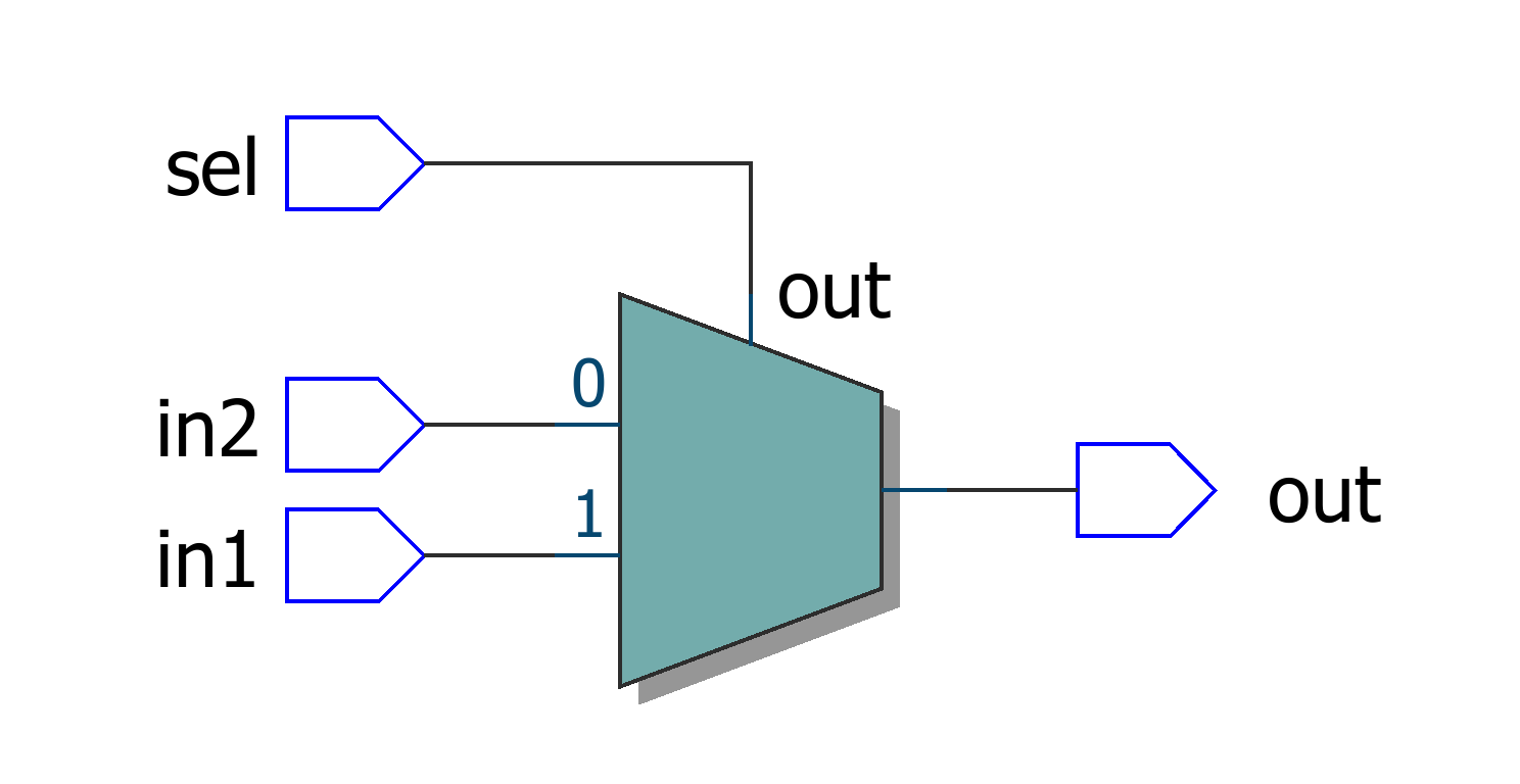
2. case语句未覆盖所有分支
生成Latch的代码:
verilog
module test (
    input wire [1:0] state,
    input wire in1,
    input wire in2,
    output reg out
);
    always @(*) begin
        case (state)
            2'b00: out = in1;
            2'b01: out = in2;
            // 没有 default 分支
        endcase
    end
endmodule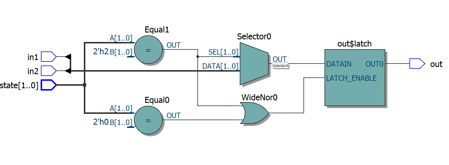
修复后的代码:
verilog
module test (
    input wire [1:0] state,
    input wire in1,
    input wire in2,
    output reg out
);
    always @(*) begin
        case (state)
            2'b00: out = in1;
            2'b01: out = in2;
            default: out = 1'b0; // 添加默认值
        endcase
    end
endmodule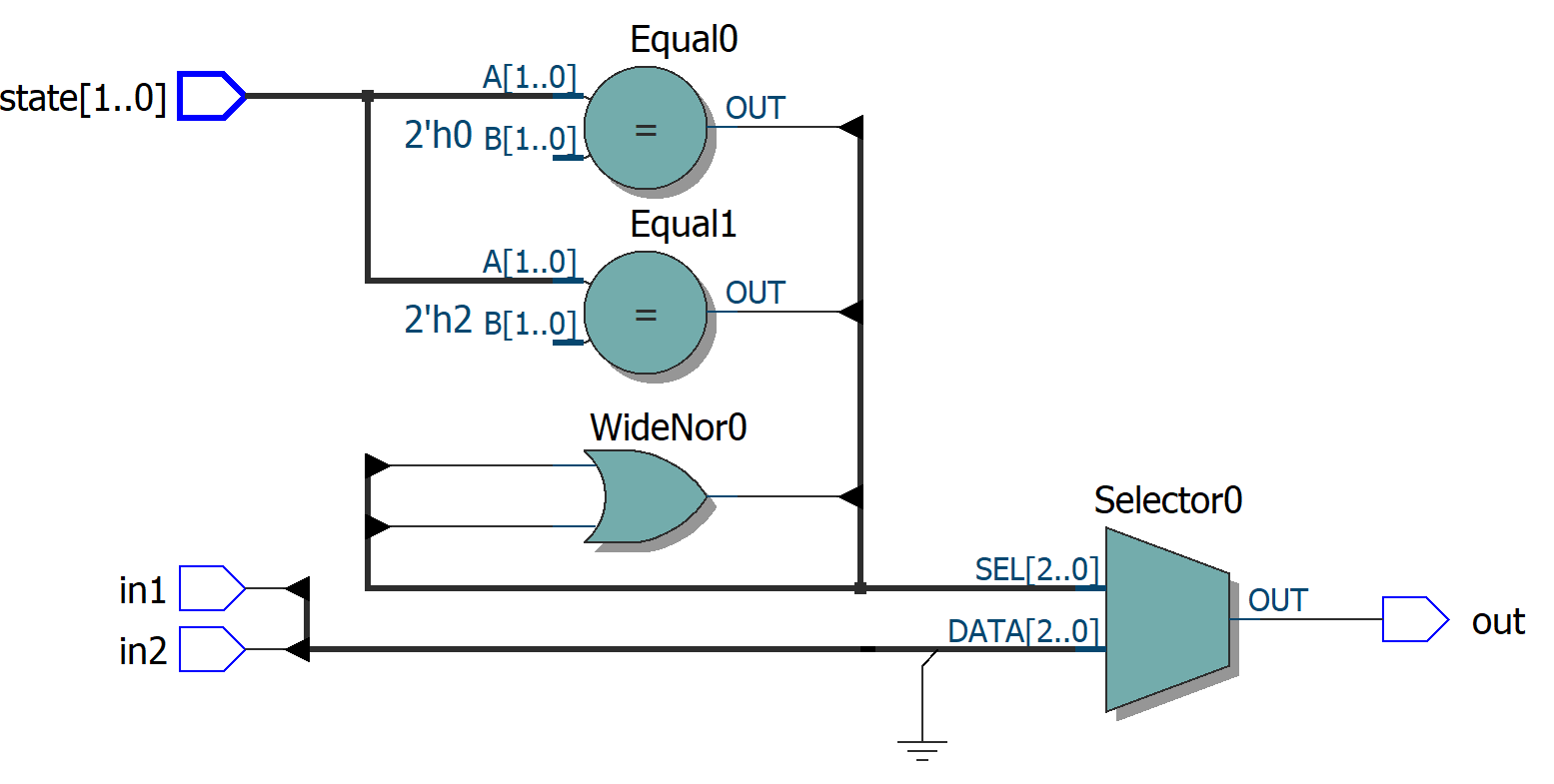
3. 组合逻辑中缺少默认赋值
生成Latch的代码:
verilog
module test (
    input wire enable,
    input wire data_in,
    output reg out
);
    always @(*) begin
        if (enable) begin
            out = data_in;
        end
        // 没有 else 分支
    end
endmodule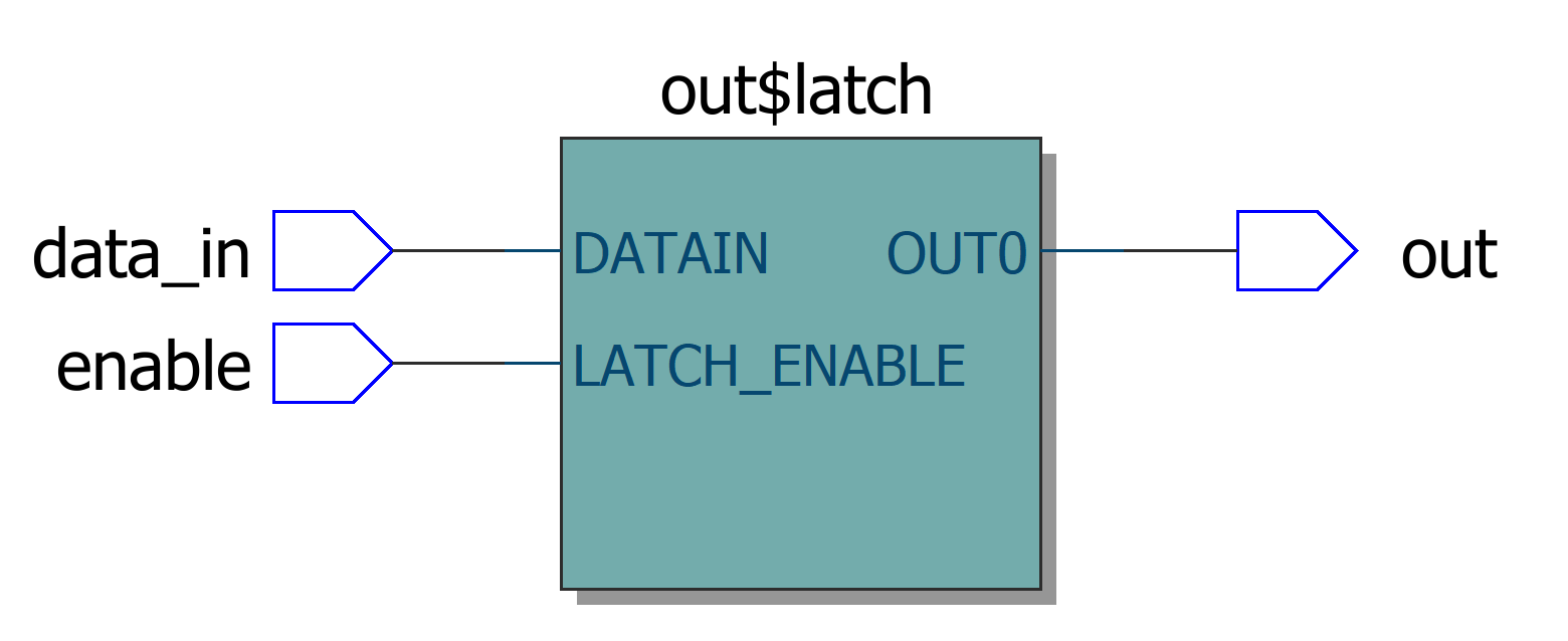
修复后的代码:
verilog
module test (
    input wire enable,
    input wire data_in,
    output reg out
);
    always @(*) begin
        out = 1'b0; // 默认值
        if (enable) begin
            out = data_in;
        end
    end
endmodule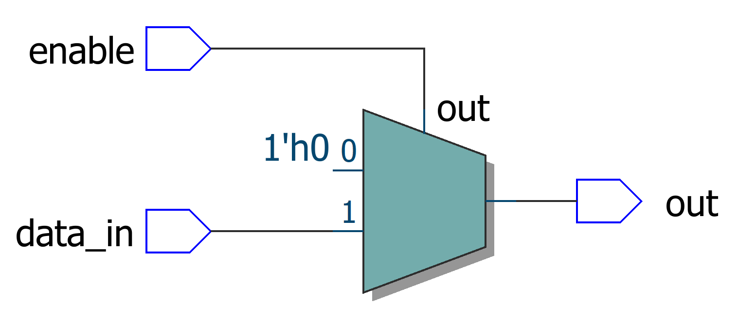
4. 多路选择器中未处理所有输入
生成Latch的代码:
verilog
module test (
    input wire [1:0] sel,
    input wire in1,
    input wire in2,
    input wire in3,
    output reg out
);
    always @(*) begin
        case (sel)
            2'b00: out = in1;
            2'b01: out = in2;
            2'b10: out = in3;
            // 没有处理 2'b11
        endcase
    end
endmodule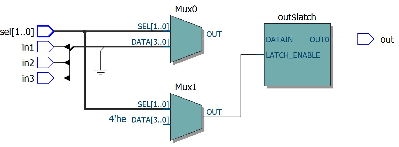
修复后的代码:
verilog
module test (
    input wire [1:0] sel,
    input wire in1,
    input wire in2,
    input wire in3,
    output reg out
);
    always @(*) begin
        case (sel)
            2'b00: out = in1;
            2'b01: out = in2;
            2'b10: out = in3;
            default: out = 1'b0; // 添加默认值
        endcase
    end
endmodule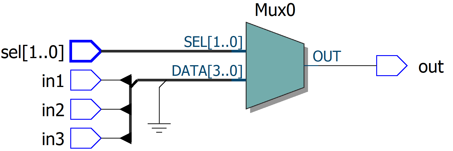
5. 部分条件未赋值
生成Latch的代码:
verilog
module test (
    input wire condition1,
    input wire condition2,
    input wire in1,
    input wire in2,
    output reg out
);
    always @(*) begin
        if (condition1) begin
            out = in1;
        end else if (condition2) begin
            out = in2;
        end
        // 没有 else 分支
    end
endmodule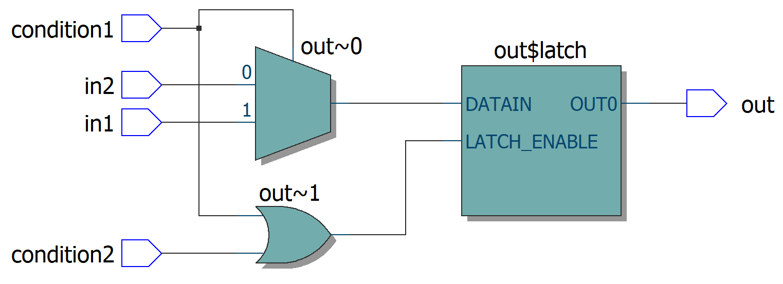
修复后的代码:
verilog
module test (
    input wire condition1,
    input wire condition2,
    input wire in1,
    input wire in2,
    output reg out
);
    always @(*) begin
        out = 1'b0; // 默认值
        if (condition1) begin
            out = in1;
        end else if (condition2) begin
            out = in2;
        end
    end
endmodule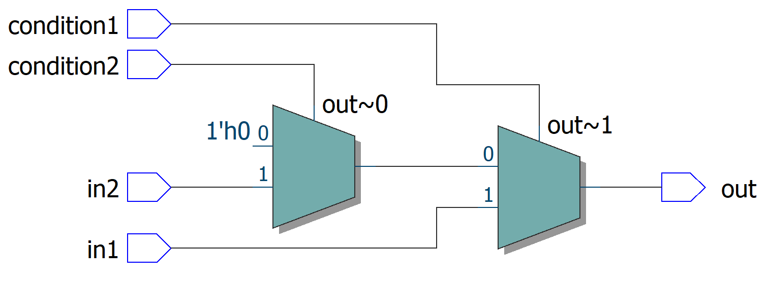
6. 反馈路径中的Latch
生成Latch的代码:
verilog
module test (
    input wire reset,
    input wire enable,
    input wire d,
    output reg q
);
    always @(*) begin
        if (reset) begin
            q = 1'b0;
        end else if (enable) begin
            q = d;
        end
        // 没有 else 分支
    end
endmodule
修复后的代码:
verilog
module test (
    input wire reset,
    input wire enable,
    input wire d,
    output reg q
);
    always @(*) begin
        q = 1'b0; // 默认值
        if (reset) begin
            q = 1'b0;
        end else if (enable) begin
            q = d;
        end
    end
endmodule