"gain and offset for ADC channel" 指的是 ADC 通道的增益 (Gain) 和偏移 (Offset),即用于校准单个 ADC 通道的两个关键参数。
🎯 基本概念
ADC 的实际转换结果并非理想的直线,通常会存在误差。其转换关系可简化为:
ADC码值 = 实际增益 × 输入电压 + 实际偏移
通过校准,可以求出这两个误差参数,并用其修正原始读数,从而得到更精确的电压值。 这个过程就是确定每个通道的 gain 和 offset。
⚙️ 参数详解
1. Offset (偏移/零点误差)
-
定义:当输入电压为 0V (或参考零点) 时,ADC 实际输出的码值与理想值 (通常是 0 或中间值) 的偏差。
-
影响:导致整个量程的零点发生平移。
-
校准:通过测量零点,计算并减去这个固定的偏差值。
2. Gain (增益/满量程误差)
-
定义:ADC 实际转换曲线的斜率与理想斜率的偏差,反映了满量程点的误差。
-
影响:导致整个量程的刻度不准,例如读数整体偏大或偏小。
-
校准:通过测量一个已知的高参考电压,计算并修正这个斜率误差。
==============
The ADC gain and offset errors can be compensated through hardware, thereby reducing the application overhead of compensating these ADC errors.
ADC增益和偏移误差可以通过硬件进行补偿,从而减少补偿这些ADC误差的应用开销。
Offset error
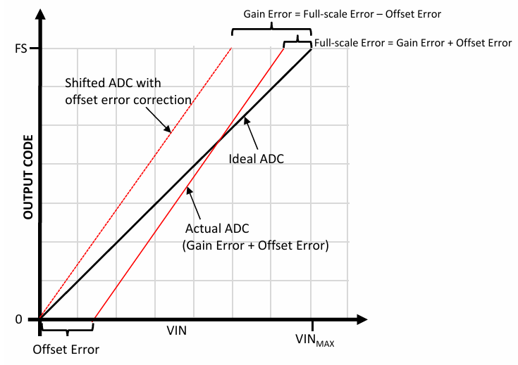
ADC Offset error is defined as the deviation between the first ideal code transition and the first actual code transition. The first ideal code transition takes place at 0.5 LSB.
ADC偏移误差被定义为第一理想码转换和第一实际码转换之间的偏差。第一个理想的代码转换发生在0.5 LSB。
If the output code is greater than zero when the input voltage is less than 0.5 LSB, the ADC has a positive offset error. ADC has a negative offset error if the first output code transition occurs when the input voltage is greater than 0.5 LSB.
如果输入电压小于0.5LSB时输出码大于零,则ADC具有正偏移误差。如果当输入电压大于0.5LSB时发生第一次输出码转换,则ADC具有负偏移误差。
Both positive and negative offset errors limit the available range of the ADC. A large positive offset error causes the ADC to saturate before the input voltage reaches maximum. A large negative offset error results in zero ADC output code for small input voltages.
正负偏移误差都限制了ADC的可用范围。较大的正偏移误差会导致ADC在输入电压达到最大值之前饱和。大的负偏移误差导致小输入电压的ADC输出代码为零。
Gain Error
Gain error is defined as the deviation of the midpoint of the last step of the ideal ADC transfer from the midpoint of the last step of the actual ADC, after the offset error is compensated.
增益误差定义为补偿偏移误差后,理想ADC传输最后一步的中点与实际ADC最后一步中点的偏差。
If the transfer function of the actual ADC results in ADC saturation before the input voltage reaches maximum, a positive gain error is produced. If the transfer function of the actual ADC is such that the ADC does not reach full-scale value when the input voltage is at maximum, a negative gain error is produced.
如果实际ADC的传递函数在输入电压达到最大值之前导致ADC饱和,则会产生正增益误差。如果实际ADC的传递函数使得ADC在输入电压最大时没有达到满标度值,则会产生负增益误差。
Gain error can also be represented as the full-scale error minus the offset error, as shown in the following graph
增益误差也可以表示为满标度误差减去偏移误差,如下图所示
Figure 2-1. Full-Scale Error, Gain Error, and Offset Error in ADC
Calibrating the Offset and Gain Errors Using a Two-Point Calibration Method
For a unipolar ADC, the input range is always positive and the output code ranges from zero to full-scale (or 0xFFF for a 12-bit ADC). However, a unipolar ADC can have both positive and negative offset errors. While it is possible to calculate (and calibrate) the positive offset error by applying zero volt input, it is not possible to calculate the negative offset error by applying zero volts to the ADC input. This is because in the case of a negative offset error, applying zero volt input will read 0x000, thereby giving a false impression that there is no offset error. Therefore, a two-point calibration method must be used and the two calibration points must be chosen such that one calibration point is slightly below 10% and the second calibration point is slightly above 90% of full-scale range.
对于单极ADC,输入范围始终为正,输出代码范围从零到满标度(对于12位ADC为0xFFF)。然而,单极ADC可能同时存在正负偏移误差。虽然可以通过施加零伏输入来计算(和校准)正偏移误差,但不可能通过向ADC输入施加零伏来计算负偏移误差。这是因为在负偏移误差的情况下,施加零伏输入将读取0x000,从而给人一种没有偏移误差的错误印象。因此,必须使用两点校准方法,并且必须选择两个校准点,使得一个校准点略低于满量程的10%,第二个校准点稍高于满量程的90%。
In this example, the two calibration points are chosen at V1 = 0.15V and V2 = 1.55V, which are at approximately 9% and 93% of the full-scale value of 1.65V.
The ideal ADC output values at V1 and V2 are represented as Ci1 and Ci2.
The actual ADC output values at V1 and V2 are represented as Ca1 and Ca2.
Using an accurate voltage source, apply V1 = 0.15V and save the actual ADC output value as Ca1. The ideal ADC output voltage Ci1 at V1 = 0.15V can be calculated as (V1 x 4096)/1.65 ≈ 372.
Similarly, apply V2 = 1.55V and save the ADC output value as Ca2. The ideal ADC value Ci2 can be calculated as (V2 x 4096)/1.65 ≈ 3847.
The gain and offset error will be calculated using the equation of a straight line y = mx + b, where m is the slope of the line and b is the offset.
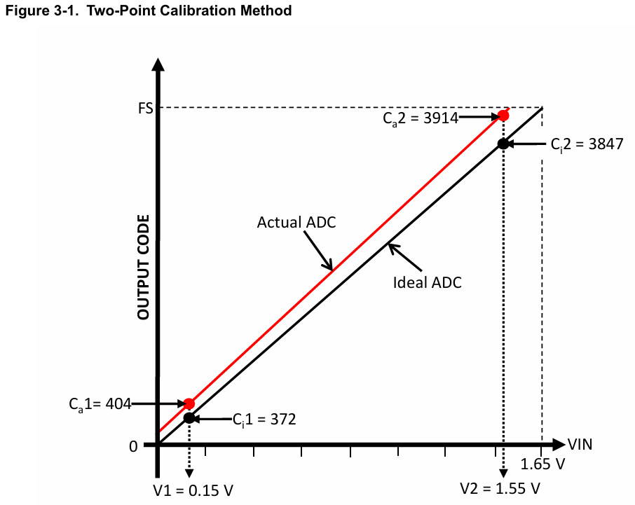
The gain error can be calculated as the slope of the actual ADC output divided by the slope of the ideal ADC output.
Gain calibration = (Ci2 - Ci1) / (Ca2-Ca1)
= (3847 -- 372) / (3914 -- 404)
= 3475 / 3510
= 0.99
Once the gain calibration is calculated, the offset calibration can be calculated as: b = y - mx, i.e. Ci = (Ca - offset calibration) * Gain calibration
Offset calibration= Ca1 - Ci1 / Gain calibration = 404 -- 372/0.99 = 28
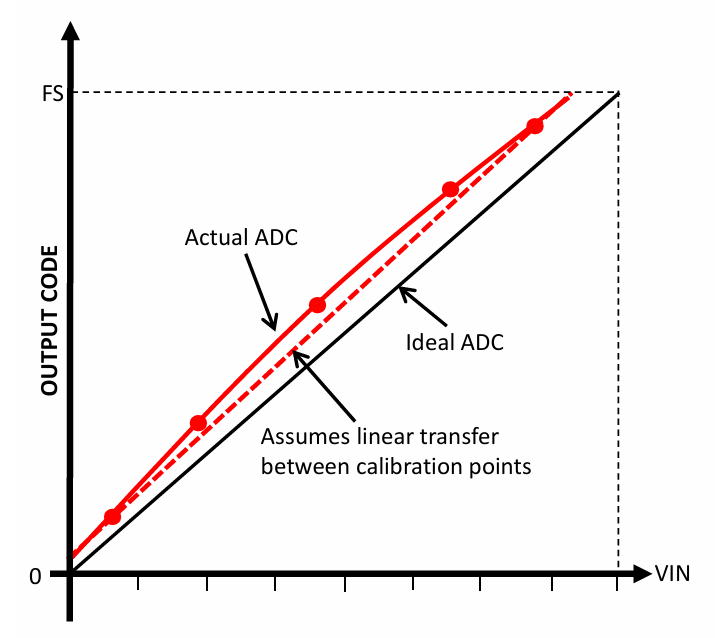
The above method of calibration assumes a straight line or a linear transfer function between the calibrated points. If the accuracy is needed over the entire range of ADC, multi-point calibration may be performed as shown in the following figure. The calibration values can be stored in a look-up table and the error can be compensated by the software at run-time. Of course, there is a trade-off between the number of calibration points, execution time and memory usage.
上述校准方法假设校准点之间为直线或线性传递函数。如果需要整个ADC范围内的精度,可以如下图所示进行多点校准。校准值可以存储在查找表中,软件可以在运行时补偿误差。当然,校准点的数量、执行时间和内存使用之间存在权衡。
Figure 3-2. Software-Based Multi-point Calibration to Compensate for Non-linearities in the ADC Transfer Function
Offset Calibration:
Apply 0V input to the ADC. Measure the ADC count. This represents the offset error of the system. Store this in the Flash and subtract this value from actual measurements.
向ADC施加0V输入。测量ADC计数。这表示系统的偏移误差。将此值存储在闪存中,并从实际测量值中减去此值。
有时是将ADC短接到GND,用此时读出来的AD值作为zero offset。
Gain Calibration:
To compensate for gain error, apply a known voltage to the ADC. Measure the ADC counts. Calculate the ratio of Input Voltage / ADC Counts. Store this value as the scale factor. During normal measurement, multiply the ADC Counts by the scale factor to get the gain compensated value.
为了补偿增益误差,向ADC施加已知电压。测量ADC计数。计算输入电压/ADC计数的比率。将此值存储为比例因子。在正常测量期间,将ADC计数乘以比例因子以获得增益补偿值。
Combining the offset and gain calibrations, the accuracy of the ADC can be improved.
结合偏移和增益校准,可以提高ADC的精度。
参考:
1,英飞凌 Infineon的knowledge base:
Offset and Gain ADC Errors and Techniques to Compensate these Errors
2, Microchip
ADC Gain and Offset Error Calibration on ARM Cortex-M0+ Based MCUs
扩展学习:
1, TI视频
Understanding and calibrating the offset and gain for ADC systems | Video | TI.com
adcs-understanding-and-calibrating-the-offset-and-gain-for-adc-systems-presentation-quiz.pdf
2,NXP