1.摘要
上一篇文章 基于FPGA的APS6404L-3SQR QSPI PSRAM驱动设计(1)主要记录了数据手册和设计中框架,这里记录一下具体的spi协议相关的设计。
在PSRAM的众多命令中有一些命令用spi协议控制更方便(我感觉)。比如两个复位命令66和99,在没配置QPI命令模式之前只能用SPI协议,所以类似复位命令这些指令如(良品检测、配置QPI和边界选择)都使用SPI来控制即可。
这些协议中除了良品检测命令其他都只是需要简单发送8bit命令,利用spi协议发送简单的一批。对于良品检测命令就需要用到状态机控制了,分别写命令+写地址+读数据了,稍微复杂一点。
2.FPGA设计
2.1、时序图设计
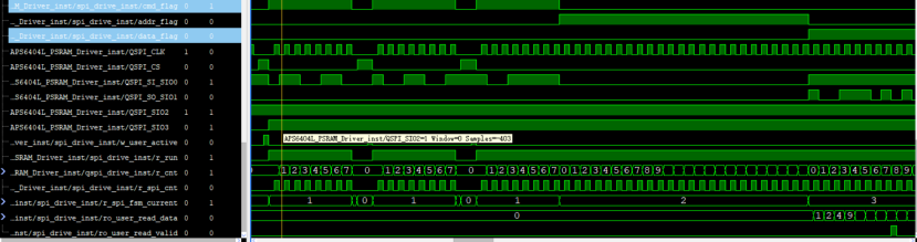
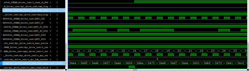
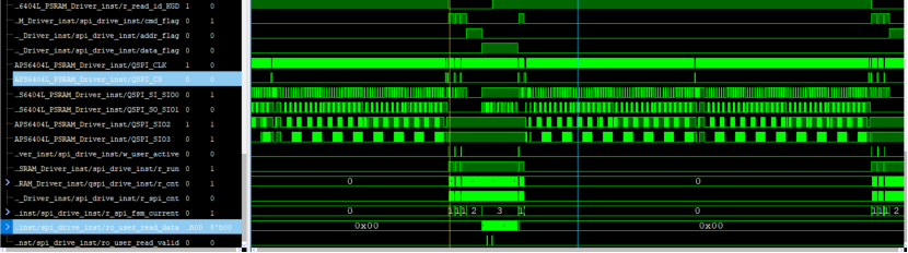
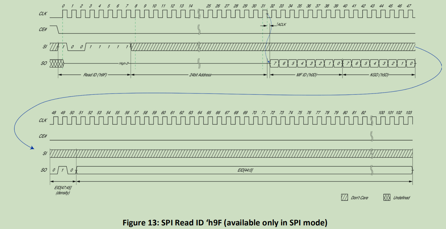
当spi模块的状态机跳转到写命令状态时,即可开始向PSRAM芯片写入命令,具体工作过程如时序图所示:
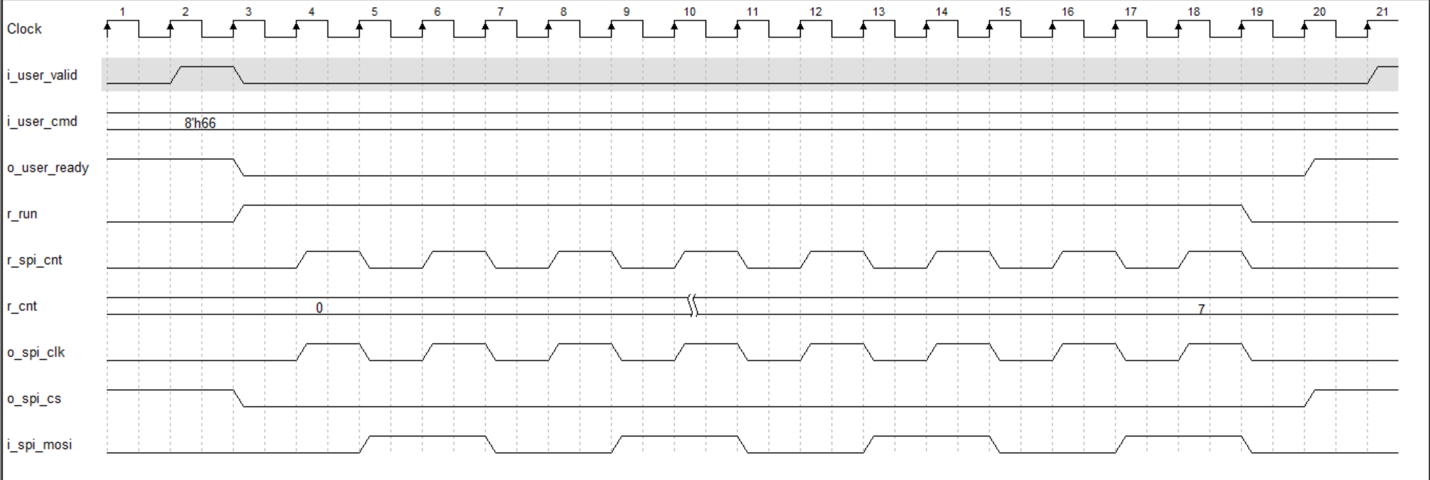
具体设计思路为:
状态机检测到命令输入立刻从IDLE跳转到SPI_CMD,同时spi工作有效信号r_run拉高。因为是8bit命令,所以计数器r_cnt计数0-7,r_spi_cnt作为计数器标志信号,通过在spi有效期内翻转实现,也就是二分频,同时也作为o_spi_clk。
当输入的命令为良品检测时,r_run信号将延迟拉低,具体时间为24bit的地址周期,加上56bit的读数据周期,最终当 r_cnt计数到88时在拉低,其余信号逻辑不变。
代码中的i_spi_8bit_cmd信号是上层模块输入的判断是否是良品检测命令,不是为1是为0。
always@(*)
begin
	if(i_rst)
		r_spi_fsm_next	<=	'd0	;
	else begin
		case (r_spi_fsm_current)
			IDLE		:
				if (w_user_active)	begin
					r_spi_fsm_next	<=	SPI_CMD	;
				end else
					r_spi_fsm_next	<=	IDLE	;
			SPI_CMD		:
				if (r_cnt == 'd7 && r_spi_cnt)
					if (i_spi_8bit_cmd)
						r_spi_fsm_next	<=	SPI_END	;
					else
						r_spi_fsm_next	<=	SPI_ADDR	;
				else
					r_spi_fsm_next	<=	SPI_CMD		;
			SPI_ADDR	:
				if (r_cnt == 'd23 && r_spi_cnt)
					r_spi_fsm_next	<=	SPI_DATA	;
				else
					r_spi_fsm_next	<=	SPI_ADDR	;
			SPI_DATA	:
				if (r_cnt == 'd55 && r_spi_cnt)
					r_spi_fsm_next	<=	SPI_END	;
				else
					r_spi_fsm_next	<=	SPI_DATA	;
			SPI_END		:
				r_spi_fsm_next	<=	IDLE	;
			default		:
				r_spi_fsm_next	<=	IDLE	;
		endcase
	end
end

always@(posedge i_clk,posedge i_rst)
begin
	if(i_rst)
		r_run <= 'd0;
	else if (r_spi_fsm_current == SPI_CMD && i_spi_8bit_cmd)	begin
		if (r_spi_cnt && r_cnt == 'd7)
			r_run 	<=	1'b0;
		else
			r_run	<=	1'b1;
	end else if (r_spi_fsm_current == SPI_DATA && r_run)	begin
		if (r_spi_cnt && r_cnt == 'd55)
			r_run	<=	1'b0	;
		else
			r_run	<=	1'b1	;
	end else if(w_user_active)
		r_run <= 'd1;
	else
		r_run <= r_run;
end

always@(posedge i_clk,posedge i_rst)
begin
	if(i_rst)
		r_cnt	<=	'd0	;
	else if (r_spi_fsm_current != r_spi_fsm_next)
		r_cnt <= 'd0;
	else if (r_run && r_spi_cnt)
		r_cnt	<=	r_cnt + 'd1	;
end

always@(posedge i_clk,posedge i_rst)
begin
	if(i_rst)
		r_spi_cnt <= 'd0;
	else if(r_run)
		r_spi_cnt <= r_spi_cnt + 1;
	else
		r_spi_cnt <= 'd0;
end
对于6线spi芯片来说,它的数据线是inout接口,所以需要添加控制信号来判断是输入还是输出。如下代码,输出一下信号用于上层模块判断。
(* PAP_MARK_DEBUG="1" *)wire    cmd_flag		=	(r_spi_fsm_current == SPI_CMD);
(* PAP_MARK_DEBUG="1" *)wire    addr_flag	=	(r_spi_fsm_current == SPI_ADDR);
(* PAP_MARK_DEBUG="1" *)wire    data_flag	=	(r_spi_fsm_current == SPI_DATA);
spi驱动模块的所有端口信号如下:
spi_drive#(
    parameter               P_DATA_WIDTH        	= 8 ,
							P_ADDR_WIDTH		= 24,
							P_READ_DATA_WIDTH   	= 8 ,
							P_CPOL              	= 0 ,
							P_CPHL              	= 0
)(
	input	wire					i_clk               ,
	input	wire					i_rst               ,

	output	wire					o_spi_clk           ,
	output	wire					o_spi_cs            ,

	input	wire					i_spi_mosi		,
	output 	wire					o_spi_miso		,
	output 	wire					o_spi_cmd_flag	,
	output 	wire					o_spi_addr_flag	,
	output 	wire					o_spi_data_flag	,

	input	wire					i_spi_8bit_cmd	,

	input	wire	[23:0]			i_user_addr			,
	input	wire	[7 :0]   		i_user_cmd        ,
	input	wire					i_user_valid        ,
	output	wire					o_user_ready        ,

    output	wire	[7:0]   		o_user_read_data    ,
    output	wire                    o_user_read_valid
);
对于读取PSRAM读取良品检测输出信号,按照时序图我们需要在读数据阶段读到的第二个字节数据作为良品与否的判断。所以当r_cnt计数到15切r_qpi_cnt为1的时候获取读到的值。具体代码如下:
always@(posedge ro_spi_clk,posedge i_rst)
begin
	if(i_rst)
		ro_user_read_data <= 'd0;
	else	if (data_flag)
		ro_user_read_data <= {ro_user_read_data[P_DATA_WIDTH - 2 : 0],i_spi_mosi};
	else
		ro_user_read_data <= 'd0;
end

always@(posedge i_clk,posedge i_rst)
begin
	if(i_rst)
		ro_user_read_valid <= 'd0;
	else if (r_spi_fsm_current == SPI_DATA && ((r_cnt == 'd7 || r_cnt == 'd15) && r_spi_cnt))
		ro_user_read_valid <= 'd1;
	else
		ro_user_read_valid <= 'd0;
end
3.上板验证
按照时序图,关于spi驱动部分正确输出良品检测通过指令8'H5D。