文章目录
1.晶圆切片
* This program shows how to find dies on a horizontally aligned wafer
*
* Display initialization
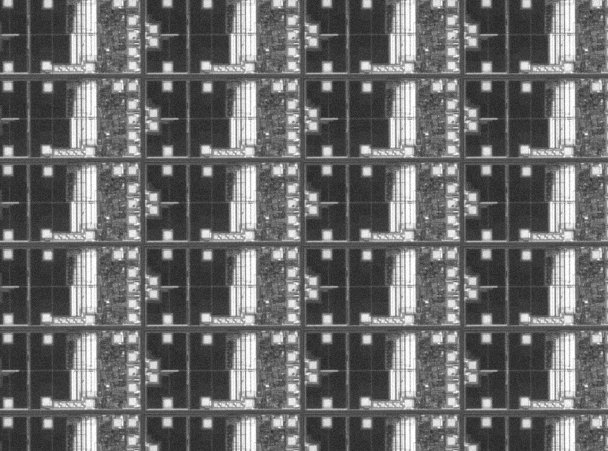
read_image (WaferDies, 'wafer_dies')
dev_close_window ()
dev_open_window_fit_image (WaferDies, 0, 0, 700, 500, WindowHandle)
set_display_font (WindowHandle, 16, 'mono', 'true', 'false')
get_window_extents (WindowHandle, WindowRow, WindowColumn, WindowWidth, WindowHeight)
dev_update_off ()
dev_set_draw ('margin')
get_image_size (WaferDies, Width, Height)
dev_display (WaferDies)
dev_disp_text ('Image of a wafer', 'window', 12, 12, 'black', [], [])
dev_disp_text ('Press Run (F5) to continue', 'window', 'bottom', 'right', 'black', [], [])
stop ()
*
* 1. Determine the size of the dies by using auto correlation
*
rft_generic (WaferDies, ImageFFT, 'to_freq', 'none', 'complex', Width)
correlation_fft (ImageFFT, ImageFFT, CorrelationFFT)
rft_generic (CorrelationFFT, Correlation, 'from_freq', 'n', 'real', Width)
* Exclude local maxima at the image border. It is sufficient
* to extract the maxima in the upper left quarter of the image because
* the autocorrelation is an even function.
gen_rectangle1 (Rectangle, 1, 1, Height / 2, Width / 2)
reduce_domain (Correlation, Rectangle, CorrelationReduced)
*
* Extract the local maxima of the auto correlation function
local_max_sub_pix (CorrelationReduced, 'gauss', 2, 5000000, Row, Col)
*
* Get the size of the dies
* Find maximum that is closest to the origin. This maximum
* corresponds to the opposite rectangle corner of the die.
distance_pp (gen_tuple_const(|Row|,0), gen_tuple_const(|Col|,0), Row, Col, Distance)
SortedIndex := sort_index(Distance)
Row1 := Row[SortedIndex[0]]
Col1 := Col[SortedIndex[0]]
DiagonalLength := sqrt(Row1 * Row1 + Col1 * Col1)
Phi := atan2(Row1,Col1)
DieWidth := DiagonalLength * cos(Phi)
DieHeight := DiagonalLength * sin(Phi)
*
* The center, the first maximum, and the second maximum
* together define the orientation and the size of the dies.
dev_set_color ('blue')
gen_cross_contour_xld (Crosses, Row, Col, 10, 0.785398)
gen_ellipse_contour_xld (Circle, Row1, Col1, 0, 12, 12, 0, 6.28318, 'positive', 1.5)
dev_display (Correlation)
dev_display (Crosses)
dev_display (Circle)
dev_set_color ('green')
dev_display (Rectangle)
dev_disp_text ('Autocorrelation, region of interest, and local maxima', 'window', 12, 12, 'black', [], [])
dev_disp_text ('Press Run (F5) to continue', 'window', 'bottom', 'right', 'black', [], [])
stop ()
*
* Visualize the extracted size of the dies
gen_rectangle2_contour_xld (Die, Height / 2, Width / 2, 0, DieWidth / 2, DieHeight / 2)
dev_display (WaferDies)
dev_set_color ('blue')
dev_display (Die)
dev_disp_text ('Extracted die size', 'window', 12, 12, 'black', [], [])
dev_disp_text ('Press Run (F5) to continue', 'window', 'bottom', 'right', 'black', [], [])
stop ()
*
* 2. Determine the position of the dies by using shape-based matching
*
LineWidth := 7
LineWidthFraction := 0.6
*
* Generate an artificial model image of the lines between the dies
gen_image_const (Template, 'byte', Width, Height)
scale_image (Template, Template, 1, 128)
RefRow := round(0.5 * Height)
RefCol := round(0.5 * Width)
for Row := -0.5 to 0.5 by 1
for Col := -0.5 to 0.5 by 1
gen_rectangle2_contour_xld (Rectangle, RefRow + Row * DieHeight, RefCol + Col * DieWidth, 0, 0.5 * DieWidth - 0.5 * LineWidth, 0.5 * DieHeight - 0.5 * LineWidth)
paint_xld (Rectangle, Template, Template, 0)
endfor
endfor
gen_rectangle2_contour_xld (Rectangle, RefRow, RefCol, 0, 0.5 * LineWidthFraction * LineWidth, DieHeight)
paint_xld (Rectangle, Template, Template, 0)
gen_rectangle2_contour_xld (Rectangle, RefRow, RefCol, 0, DieWidth, 0.5 * LineWidthFraction * LineWidth)
paint_xld (Rectangle, Template, Template, 0)
gen_rectangle2 (ROI, RefRow, RefCol, 0, DieWidth + 5, DieHeight + 5)
reduce_domain (Template, ROI, TemplateReduced)
create_shape_model (TemplateReduced, 'auto', 0, 0, 'auto', 'auto', 'ignore_local_polarity', 'auto', 5, ModelID)
dev_display (Template)
dev_set_color ('blue')
dev_display (ROI)
dev_disp_text ('Template of 4 adjacent dies', 'window', 12, 12, 'black', [], [])
dev_disp_text ('Press Run (F5) to continue', 'window', 'bottom', 'right', 'black', [], [])
stop ()
*
* Find the best instance of the artifical model in the original image
MinScore := 0.7
Greediness := 0.5
NumMatches := 1
find_shape_model (WaferDies, ModelID, 0, 0, MinScore, NumMatches, 0.5, 'least_squares', 0, Greediness, MatchRow, MatchColumn, MatchAngle, MatchScore)
*
get_shape_model_contours (ModelContours, ModelID, 1)
vector_angle_to_rigid (0, 0, 0, MatchRow, MatchColumn, MatchAngle, HomMat2D)
affine_trans_contour_xld (ModelContours, ContoursAffinTrans, HomMat2D)
dev_display (WaferDies)
dev_set_color ('blue')
dev_display (ContoursAffinTrans)
dev_disp_text ('Best match', 'window', 12, 12, 'black', [], [])
dev_disp_text ('Press Run (F5) to continue', 'window', 'bottom', 'right', 'black', [], [])
stop ()
*
* 3. Compute the cutting lines based on the size
* and the position of the dies
*
dev_clear_window ()
dev_display (WaferDies)
dev_set_color ('blue')
NumRowMax := ceil(Height / DieHeight)
NumColMax := ceil(Width / DieWidth)
for RowIndex := -NumRowMax to NumRowMax by 1
RowCurrent := MatchRow + RowIndex * DieHeight
gen_contour_polygon_xld (CuttingLine, [RowCurrent,RowCurrent], [0,Width - 1])
dev_display (CuttingLine)
endfor
for ColIndex := -NumColMax to NumColMax by 1
ColCurrent := MatchColumn + ColIndex * DieWidth
gen_contour_polygon_xld (CuttingLine, [0,Height - 1], [ColCurrent,ColCurrent])
dev_display (CuttingLine)
endfor
dev_disp_text ('Resulting cutting lines', 'window', 12, 12, 'black', [], [])
dev_disp_text (' End of program ', 'window', 'bottom', 'right', 'black', [], [])
2.算子加注释
* ============================================================
* 晶圆芯片(Wafer Dies)检测与切割线计算程序
* 功能:自动识别水平排列的晶圆芯片,确定尺寸和位置,生成切割线
* ============================================================

* ==================== 显示初始化 ====================

read_image (WaferDies, 'wafer_dies')
* 读取示例晶圆图像到变量 WaferDies

dev_close_window ()
* 关闭所有已打开的图形窗口,避免窗口堆积

dev_open_window_fit_image (WaferDies, 0, 0, 700, 500, WindowHandle)
* 根据图像尺寸打开自适应窗口(最大 700×500),返回窗口句柄 WindowHandle

set_display_font (WindowHandle, 16, 'mono', 'true', 'false')
* 设置窗口字体:16号、等宽(mono)、粗体、非斜体

get_window_extents (WindowHandle, WindowRow, WindowColumn, WindowWidth, WindowHeight)
* 获取窗口的位置(左上角行列坐标)和尺寸(宽、高)

dev_update_off ()
* 关闭自动刷新,避免每次操作都重绘画面,提升性能

dev_set_draw ('margin')
* 设置绘图模式为 margin(只画轮廓边缘),而非 fill(填充)

get_image_size (WaferDies, Width, Height)
* 获取图像的宽度 Width 和高度 Height(像素)

dev_display (WaferDies)
* 在窗口中显示晶圆图像

dev_disp_text ('Image of a wafer', 'window', 12, 12, 'black', [], [])
* 在窗口左上角 (12,12) 显示黑色说明文字

dev_disp_text ('Press Run (F5) to continue', 'window', 'bottom', 'right', 'black', [], [])
* 在窗口右下角显示"按 F5 继续"提示

stop ()
* 暂停程序执行,等待用户按 F5 继续

* ============================================================
* 第一步:通过自相关(Auto Correlation)确定芯片尺寸
* 原理:晶圆具有周期性结构,自相关图中除原点外的第一个
*        峰值位置对应芯片的周期性间距
* ============================================================

rft_generic (WaferDies, ImageFFT, 'to_freq', 'none', 'complex', Width)
* 对图像做实数傅里叶变换(RFT),从空间域转到频率域
* 输出 ImageFFT 为复数类型

correlation_fft (ImageFFT, ImageFFT, CorrelationFFT)
* 在频率域计算图像与自身的互相关(即自相关)
* 频域乘法等价于空间域卷积

rft_generic (CorrelationFFT, Correlation, 'from_freq', 'n', 'real', Width)
* 将频域的自相关结果反变换回空间域
* 输出 Correlation 为实数类型

* 排除图像边界的伪极大值。
* 由于自相关是偶函数(关于原点对称),
* 只需在左上四分之一区域提取极大值即可。

gen_rectangle1 (Rectangle, 1, 1, Height / 2, Width / 2)
* 生成矩形区域,覆盖图像左上四分之一
* 行范围:1 → Height/2,列范围:1 → Width/2

reduce_domain (Correlation, Rectangle, CorrelationReduced)
* 将自相关图的计算域裁剪到该矩形区域
* 排除边界处的干扰极大值

* 提取自相关函数的局部极大值(亚像素精度)

local_max_sub_pix (CorrelationReduced, 'gauss', 2, 5000000, Row, Col)
* 用高斯拟合以亚像素精度提取局部极大值
* 'gauss':高斯插值方法
* 2:平滑参数
* 5000000:最大返回点数
* 返回所有峰值的行列坐标 Row, Col

* 获取芯片尺寸
* 找到离原点最近的极大值,该极大值对应芯片对角线的另一端点

distance_pp (gen_tuple_const(|Row|,0), gen_tuple_const(|Col|,0), Row, Col, Distance)
* 计算每个峰值点到原点 (0,0) 的欧几里得距离
* |Row| 是峰值点总数,gen_tuple_const 生成等长的零向量

SortedIndex := sort_index(Distance)
* 按距离从小到大排序,返回排序后的索引数组

Row1 := Row[SortedIndex[0]]
* 取距离原点最近的峰值的行坐标

Col1 := Col[SortedIndex[0]]
* 取距离原点最近的峰值的列坐标

DiagonalLength := sqrt(Row1 * Row1 + Col1 * Col1)
* 计算该峰值到原点的距离,即芯片的对角线长度

Phi := atan2(Row1, Col1)
* 计算峰值相对于原点的角度(弧度),确定芯片的旋转方向

DieWidth := DiagonalLength * cos(Phi)
* 芯片宽度 = 对角线 × cos(角度),即水平方向投影

DieHeight := DiagonalLength * sin(Phi)
* 芯片高度 = 对角线 × sin(角度),即垂直方向投影

* 中心点、第一极大值和第二极大值共同定义芯片的方向和尺寸

dev_set_color ('blue')
* 设置绘图颜色为蓝色

gen_cross_contour_xld (Crosses, Row, Col, 10, 0.785398)
* 在每个局部极大值位置生成十字标记轮廓
* 10:十字大小;0.785398(≈π/4):十字旋转角度

gen_ellipse_contour_xld (Circle, Row1, Col1, 0, 12, 12, 0, 6.28318, 'positive', 1.5)
* 在最近峰值处生成圆形轮廓(长短轴均为12的椭圆,角度0→2π)
* 用于标记该关键点

dev_display (Correlation)
* 显示自相关图

dev_display (Crosses)
* 叠加显示所有十字标记

dev_display (Circle)
* 叠加显示最近峰值处的圆形标记

dev_set_color ('green')
* 切换绘图颜色为绿色

dev_display (Rectangle)
* 显示之前定义的感兴趣区域(左上四分之一矩形)

dev_disp_text ('Autocorrelation, region of interest, and local maxima', 'window', 12, 12, 'black', [], [])
* 在窗口左上角显示说明文字

dev_disp_text ('Press Run (F5) to continue', 'window', 'bottom', 'right', 'black', [], [])
* 右下角提示按 F5 继续

stop ()
* 暂停,等待用户确认

* 可视化提取的芯片尺寸

gen_rectangle2_contour_xld (Die, Height / 2, Width / 2, 0, DieWidth / 2, DieHeight / 2)
* 以图像中心为基准,生成表示单个芯片的旋转矩形轮廓
* 0:旋转角度;半宽半高分别为 DieWidth/2 和 DieHeight/2

dev_display (WaferDies)
* 重新显示原始晶圆图像

dev_set_color ('blue')
* 设为蓝色

dev_display (Die)
* 显示提取出的芯片尺寸矩形

dev_disp_text ('Extracted die size', 'window', 12, 12, 'black', [], [])
* 显示说明文字

dev_disp_text ('Press Run (F5) to continue', 'window', 'bottom', 'right', 'black', [], [])
* 提示继续

stop ()
* 暂停

* ============================================================
* 第二步:通过形状匹配(Shape-Based Matching)确定芯片位置
* 原理:人工构造一个"井"字形模板(模拟芯片间分割线),
*        然后在原图中搜索该模板的最佳匹配位置
* ============================================================

LineWidth := 7
* 定义芯片间分割线的宽度为 7 像素

LineWidthFraction := 0.6
* 分割线中实际线条占线宽的比例为 60%

* 生成人工模板图像(模拟4个相邻芯片之间的分割线)

gen_image_const (Template, 'byte', Width, Height)
* 创建一个全零的字节类型空白图像作为模板

scale_image (Template, Template, 1, 128)
* 灰度线性变换:g' = 1×g + 128
* 将整幅图变为灰度值 128(中灰色背景)

RefRow := round(0.5 * Height)
* 取图像中心行坐标作为参考原点

RefCol := round(0.5 * Width)
* 取图像中心列坐标作为参考原点

for Row := -0.5 to 0.5 by 1
* 外层循环:行方向偏移,取 -0.5 和 +0.5(上方和下方)
    for Col := -0.5 to 0.5 by 1
    * 内层循环:列方向偏移,取 -0.5 和 +0.5(左方和右方)
        gen_rectangle2_contour_xld (Rectangle, RefRow + Row * DieHeight, RefCol + Col * DieWidth, 0, 0.5 * DieWidth - 0.5 * LineWidth, 0.5 * DieHeight - 0.5 * LineWidth)
        * 在4个相邻芯片的中心位置各生成一个矩形轮廓
        * 表示芯片内部区域(减去线宽后的内框)
        paint_xld (Rectangle, Template, Template, 0)
        * 将矩形轮廓绘制到模板图像上,灰度值为0(黑色)
        * 模拟芯片间的暗色分割线
    endfor
endfor
* 循环结束后,模板上有4个相邻芯片的轮廓

gen_rectangle2_contour_xld (Rectangle, RefRow, RefCol, 0, 0.5 * LineWidthFraction * LineWidth, DieHeight)
* 在中心生成一条垂直线条轮廓,模拟垂直方向的分割线

paint_xld (Rectangle, Template, Template, 0)
* 将垂直线画到模板上(黑色)

gen_rectangle2_contour_xld (Rectangle, RefRow, RefCol, 0, DieWidth, 0.5 * LineWidthFraction * LineWidth)
* 在中心生成一条水平线条轮廓,模拟水平方向的分割线

paint_xld (Rectangle, Template, Template, 0)
* 将水平线画到模板上(黑色)

* 此时模板呈"井"字形 ------ 4个芯片被十字线分隔

gen_rectangle2 (ROI, RefRow, RefCol, 0, DieWidth + 5, DieHeight + 5)
* 生成比单个芯片稍大(各方向多5像素)的矩形 ROI 区域

reduce_domain (Template, ROI, TemplateReduced)
* 将模板裁剪到 ROI 区域,排除多余背景

create_shape_model (TemplateReduced, 'auto', 0, 0, 'auto', 'auto', 'ignore_local_polarity', 'auto', 5, ModelID)
* 基于裁剪后的模板创建形状匹配模型
* 'auto':自动确定金字塔层级
* 0, 0:起始角度和角度范围(无旋转变化)
* 'ignore_local_polarity':忽略局部极性,适应亮度反转
* 5:轮廓点数(自动)
* 返回模型 ID → ModelID

dev_display (Template)
* 显示生成的模板图像

dev_set_color ('blue')
* 设为蓝色

dev_display (ROI)
* 显示 ROI 区域

dev_disp_text ('Template of 4 adjacent dies', 'window', 12, 12, 'black', [], [])
* 显示说明文字

dev_disp_text ('Press Run (F5) to continue', 'window', 'bottom', 'right', 'black', [], [])
* 提示继续

stop ()
* 暂停

* 在原始图像中搜索人工模型的最佳匹配实例

MinScore := 0.7
* 最低匹配分数阈值为 0.7(满分 1.0),低于此值的结果被忽略

Greediness := 0.5
* 贪心系数为 0.5,平衡搜索速度和准确性
* 值越大越快但可能漏检

NumMatches := 1
* 只返回最佳的 1 个匹配结果

find_shape_model (WaferDies, ModelID, 0, 0, MinScore, NumMatches, 0.5, 'least_squares', 0, Greediness, MatchRow, MatchColumn, MatchAngle, MatchScore)
* 在晶圆图像中搜索形状模型的最佳实例
* 0, 0:搜索角度范围(无旋转搜索)
* 0.5:亚像素精度
* 'least_squares':用最小二乘法精化位置
* 返回:匹配位置 (MatchRow, MatchColumn)、角度 MatchAngle、分数 MatchScore

get_shape_model_contours (ModelContours, ModelID, 1)
* 从模型中提取轮廓,用于后续可视化
* 1:金字塔第1层

vector_angle_to_rigid (0, 0, 0, MatchRow, MatchColumn, MatchAngle, HomMat2D)
* 计算刚体变换矩阵(平移 + 旋转)
* 将模型坐标系的原点 (0,0,0) 变换到匹配位置 (MatchRow, MatchColumn, MatchAngle)

affine_trans_contour_xld (ModelContours, ContoursAffinTrans, HomMat2D)
* 用该变换矩阵将模型轮廓变换到匹配位置,得到实际位置上的轮廓

dev_display (WaferDies)
* 显示原始晶圆图像

dev_set_color ('blue')
* 设为蓝色

dev_display (ContoursAffinTrans)
* 叠加显示匹配位置的轮廓

dev_disp_text ('Best match', 'window', 12, 12, 'black', [], [])
* 显示说明文字

dev_disp_text ('Press Run (F5) to continue', 'window', 'bottom', 'right', 'black', [], [])
* 提示继续

stop ()
* 暂停

* ============================================================
* 第三步:根据芯片尺寸和位置计算切割线
* 原理:以匹配位置为锚点,按芯片宽高等间距向四周
*        延伸,生成覆盖整幅图像的网格切割线
* ============================================================

dev_clear_window ()
* 清空窗口

dev_display (WaferDies)
* 重新显示原始晶圆图像

dev_set_color ('blue')
* 设为蓝色绘图

NumRowMax := ceil(Height / DieHeight)
* 计算行方向需要的最大切割线数量(向上取整,确保覆盖全图)

NumColMax := ceil(Width / DieWidth)
* 计算列方向需要的最大切割线数量(向上取整)

for RowIndex := -NumRowMax to NumRowMax by 1
* 遍历行方向的切割线索引(从负到正,覆盖整个图像)
    RowCurrent := MatchRow + RowIndex * DieHeight
    * 计算当前水平切割线的行位置
    * 以匹配点为基准,按芯片高度等间距偏移
    gen_contour_polygon_xld (CuttingLine, [RowCurrent,RowCurrent], [0,Width - 1])
    * 生成一条水平切割线轮廓,从左边缘(0)到右边缘(Width-1)
    dev_display (CuttingLine)
    * 显示该水平切割线
endfor

for ColIndex := -NumColMax to NumColMax by 1
* 遍历列方向的切割线索引
    ColCurrent := MatchColumn + ColIndex * DieWidth
    * 计算当前垂直切割线的列位置
    gen_contour_polygon_xld (CuttingLine, [0,Height - 1], [ColCurrent,ColCurrent])
    * 生成一条垂直切割线轮廓,从上边缘(0)到下边缘(Height-1)
    dev_display (CuttingLine)
    * 显示该垂直切割线
endfor

dev_disp_text ('Resulting cutting lines', 'window', 12, 12, 'black', [], [])
* 显示说明文字"切割线结果"

dev_disp_text ('      End of program      ', 'window', 'bottom', 'right', 'black', [], [])
* 右下角显示"程序结束"