ver0.1
前言
前面的文章我们对ARM体系下电源管理的系统架构和软件架构的核心内容做了介绍,对PE-Core的Idle管理机制PSCI也做了充分的分析,而OSPM对于PE-Core的电源管理还有一个重要的分支就是DVFS,也就是通过OSPM干预的手段最大程度的提升PE-Core的效能。本文将围绕DVFS这个课题展开讨论,带大家搞清楚DVFS相关的系统架构,为我们后续讨论OSPM的调度(性能)管理等打下硬件方面基础。同样在阅读本文之前,希望大家读一读我们的前序文章,掌握一些基础,也顺便找找感觉:
(4)A-25ARMv8/v9-GIC的系统架构(中断的硬件基础)
(5)A-38ARMv8/v9-Generic Timer系统架构
(6)A-41ARMv9/v8-电源管理系统架构(Power Management System Architecture)
(7)A-42ARMv9/v8-电源管理工作原理(SCP Service Overview)
(8)A-43ARMv9/v8-电源控制框架简介PCF(Power Control Framework Overview)
(9)A-0x2cARMv9/v8-电源管理域(Voltage Domain/Power Domain)
(10)A-45ARMv9/v8-电源模式(Power Modes)
(11)A-46ARMv9/v8-电源状态(Power States)
(12)V-05 虚拟化基础-异常模型(Exception)(AArch64)
(13)A-47ARMv9/v8-电源状态管理软件架构(PSCI架构)
(14)A-48ARMv9/v8-电源状态管理机制(PSCI协调机制)
(15)A-49ARMv9/v8-PSCI接口规范与工作流程简介
正文
1.1 背景
还记得我们介绍OSPM是如何在PSCA的体系下干预电源管的吗:
OSPM for AP cores can be broadly classified into idle management, and dynamic voltage and frequency scaling (DVFS) frameworks. As shown in Figure 1-0, these frameworks are associated with the scheduling in the OS. However, it should be noted that the association between the scheduler and the OSPM frameworks might only be a loose coupling.
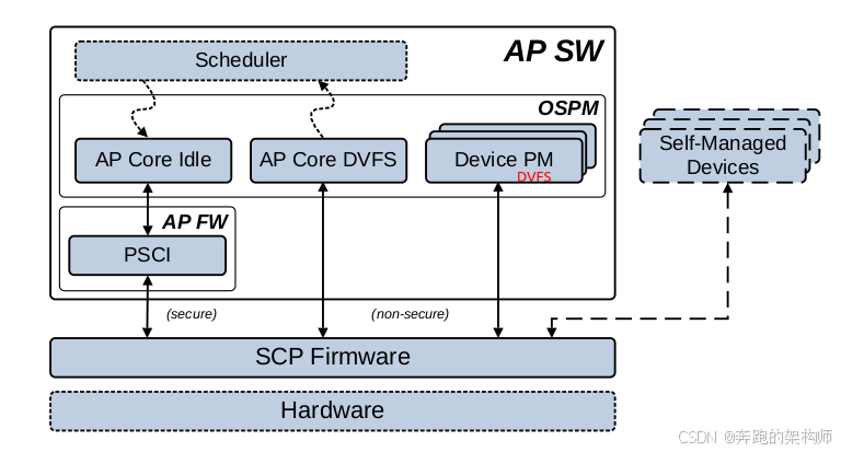
图1-0 Simplified power management software stack
本文我们将站在系统架构的视角完成对PSCA体系下,DVFS相关内容的讨论。主要集中在系统架构层面,软件层面的讨论会穿插一些,核心的DVFS软件模块会结合具体的OS(Linux)留在后续的文章中和大家分享。
1.2 DVFS的相关组件
1.2.1 SCP-DVFS的核心枢纽
先看一下PSCA架构下的核心节点SCP,如图1-1所示。
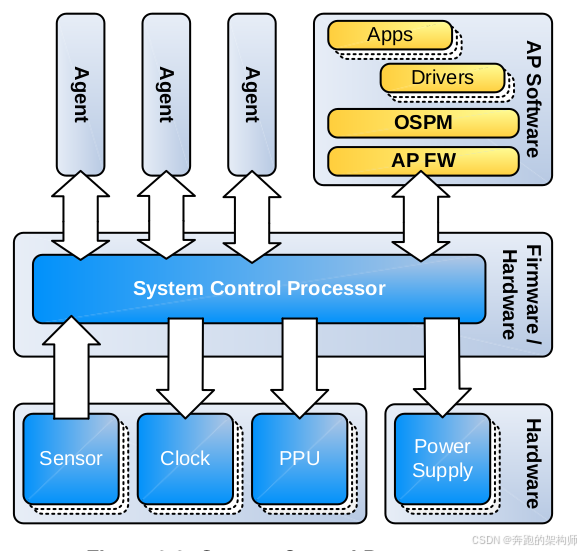
图1-1 System Control Processor concept
SCP对基于ARM体系的SOC的电源管理主要的四个抓手就是Sensor、Clock、Processor、Power Supply,而被管理的对象就是SOC上面的各个Agent,包裹CPU也是Agent。SCP的业务有很多其中就有如下两个方面:
Voltage Regulator Control
The SCP manages voltage supplies for functions including post-boot switch-on, switch off and DVFS voltage level changes.
The voltage supplies are typically provided by a separate power management IC. The voltage regulator control component provides the interface for this function. The protocol of the interface is implementation specific dependent on the choice of power management IC.
Clock Control
The SCP does not control run time dynamic gating of clocks at component activity level. This is managed by clock controllers with hardware autonomous Q-Channel management.
The SCP manages clock source enabling, selection, and division. Clock sources might include off chip sources, such as crystal oscillators, and on-chip sources such as PLLs. Each clock source will typically be able to be divided to produce a multitude of frequencies for different components.together
These settings might be static, set up once when a component is required or powered up, or changed at the request of the component or related software, such as for AP or GPU DVFS.
通过上面的描述我们简单的归纳两点:
(1) SCP 对于系统内部各个Agent的电压的控制内容包括:启动、关闭、电压等级的调节(DVFS voltage level changes)。而ARM在PSCA的集成手册中也给出了调节电压的组件的介绍如图1-2所示:
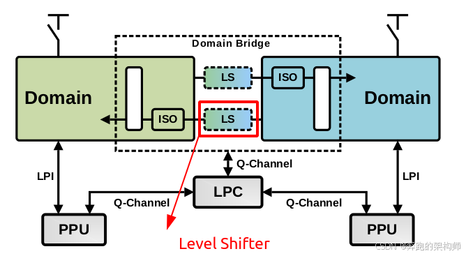
图1-2 Voltage Level Shifter
看一下手册中对LS的介绍:
When crossing between voltage domains, level shifters must be placed between the two domains to manage the difference in voltage levels between the two voltage supplies. Closing timing across such a boundary is difficult because of the considerable number of voltage-supply cross corners that need to be analyzed. Therefore, it is treated as an asynchronous interface for all signals.
(2) SCP 对Clock的管理主要包括时钟源的使能、选择、分频。PSCA体系下对于时钟管理的框架如图1-3所示:
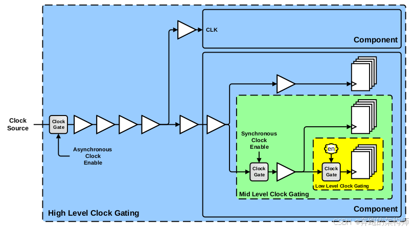
图1-3 Clock gating hierarchy
看一下手册的描述,核心的观点就是通过分级的时钟管理架构,可以更加灵活和高效的通过时钟控制SOC内部各个电源域的电源表现,这一部分就不展开讨论了:
There can be multiple levels of clock gating within a system. This specification uses the following classification:
• Low-Level: Clock gates inserted automatically by synthesis tools.
• Mid-Level: Instantiated clock gating, typically synchronously controlled, within components.
• High-Level: Instantiated gating of entire clock domains.
These clock gating levels are all complementary and should be implemented regardless of the presence of other levels within the structure. Each level has benefits with different levels of power saving and temporal granularity.
通过上面的描述,可以看出PSCA的框架中是支持电压等级和时钟频率的动态调节,这也就为我们继续讨论DVFS打下了硬件基础。
1.2.2 PE-Cores-DVFS的操作对象
对于ARM的CPU来说,OSPM就是通过DVFS的调节来是PE-Cores达到最佳能效:
Many systems operate under conditions where their workload is variable. Therefore it is useful to be able to reduce or increase the core performance to match the expected core workload.
Clocking the core more slowly reduces dynamic power consumption.
Dynamic Voltage and Frequency Scaling (DVFS) is an energy saving technique that exploits:
• The linear relationship between power consumption and operational frequency.
• The quadratic relationship between power consumption and operational voltage. This relationship is given as:
P = C × V × V × f
Where:
P Is the dynamic power.
C Is the switching capacitance of the logic circuit in question.
V Is the operational voltage.
f Is the operational frequency.
Power savings are achieved by adjusting the frequency of a core clock.
At lower frequencies, the core can also operate at lower voltages. The advantage of reducing supply voltage is that it reduces both dynamic and static power.
There is an IMPLEMENTATION SPECIFIC relationship between the operational voltage for a given circuit and the range of frequencies that circuit can safely operate at. A given frequency of operation together with its corresponding operational voltage is expressed as a tuple and is known as an Operating Performance Point (OPP). For a given system, the range of attainable OPPs is collectively termed as the system DVFS curve.
Operating systems use DVFS to save energy and, where necessary, keep within thermal limits. The OS provides DVFS policies to manage the power consumed and the required performance. A policy that is aimed at high performance selects higher frequencies and uses more energy. A policy that is aimed at saving energy selects lower frequencies and therefore results in lower performance.
通过上马的公式可以看出,一个工作电压一个工作频率直接决定了ARM CPU的功耗,这里我们围绕电压和时钟的调节归纳如下:
(1) 首先ARM的CPU要实现PSCA框架的基础组件,使每一个PE-Core都支持在运行时被SCP进行DVFS的调节,这里我们以DSU为例进行讲解。
• 电压调节
电压的调节是以电压域为单位展开,如图1-4所示:
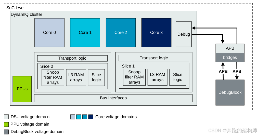
图1-4 DSU-120 voltage domains
节选DSU手册中的部分描述:
The power management techniques employed by the DSU-120 and cores in the cluster include:
• Power Policy Units (PPUs) providing autonomous power management of the L3 cache and the cores
• Support for cores running independently at different frequencies and voltages known as Dynamic Voltage Frequency Scaling (DVFS). For cores in a complex, DVFS is only possible for the whole complex, not for individual cores.
• Per-core Dynamic Voltage and Frequency Scaling (DVFS)
• Having each core in a separate voltage domain allows Dynamic Voltage Frequency Scaling (DVFS) to be applied to each core.
这部分其实就很好理解了,DSU这个Cluster和这个Cluster下的PE-Cores根据不同的组合或者按照个体或者按照组都支持DVFS的调节,而进行电压调节的基础就是要将这些PE-Core置于不同的电压域内。
• 时钟调节
电压调节的基础已经有了,该轮到时钟了,如图1-5所示:
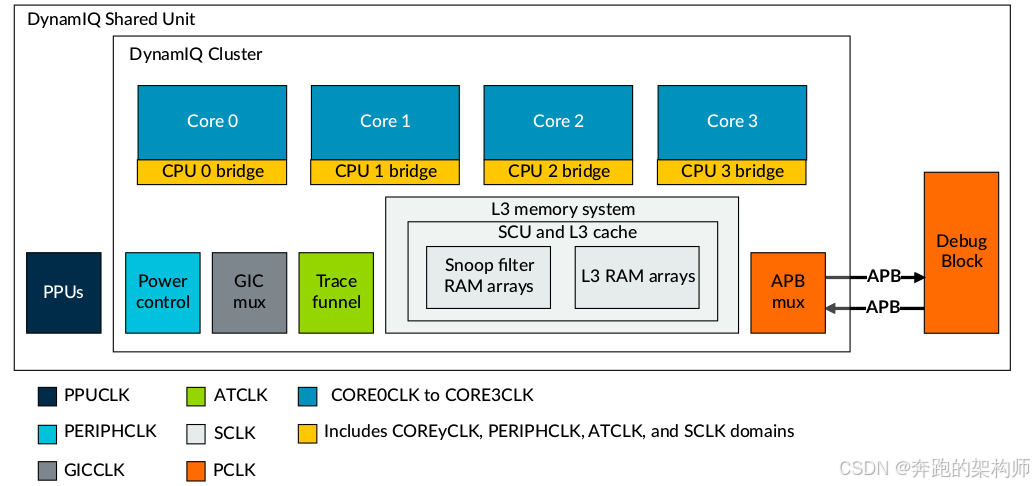
图1-5 DSU-120 clock domains
看一下手册的描述:
The DynamIQ ™ Shared Unit-120 (DSU-120) has multiple clock domains. Each core or complex can be implemented in a separate clock domain.
The cluster contains several clock domains for functionality that is likely to be connected to different clocks in the system. Within each core, the CPU bridge contains asynchronous bridges for all crossings between the core and cluster clock domains.
ARM将DSU内部的每个组件都归到一个时钟域内,不同的时钟信号作用自然也不相同,如图1-6所示:
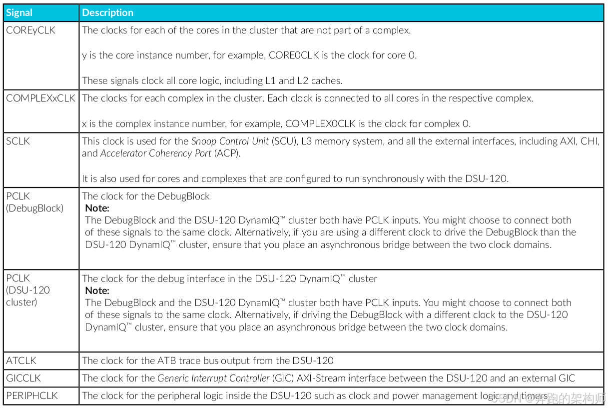
图1-6 DSU-120 clock signals
结合图1-5、1-6,我们重点关注一下与PE-Core相关的时钟:
While there is no functional requirement for any of the clocks to have any relationship to any of the others, the DSU-120 is designed with the following expectations to achieve an acceptable performance:
• The COREyCLK or COMPLEXxCLK can be dynamically scaled to match the performance requirements of that core.
• SCLK is recommended to run between the maximum COREyCLK or COMPLEXxCLK frequency and approximately half of the maximum COREyCLK or COMPLEXxCLK frequency.
• SCLK can run at synchronous 1:1 or 2:1 frequencies with the external interconnect, avoiding the need for an asynchronous bridge between them.
• The frequency of ATCLK must be determined based on the trace bandwidth of the system.
• GICCLK can be run at the same frequency as the interrupt controller that it connects to. This would typically be approximately 25% of the maximum COREyCLK or COMPLEXxCLK frequency.
• PCLK can run at the same frequency as the debug subsystem that it connects to. This would typically be approximately 25% of the maximum COREyCLK or COMPLEXxCLK frequency.
• The PERIPHCLK domain contains the architectural timers, and software performance can be impacted if reads to these registers take too long. Therefore, Arm ® recommends that the PERIPHCLK frequency is at least 25% of the maximum COREyCLK or COMPLEXxCLK frequency.
• Arm ® recommends that the PPUCLK clock frequency is at least 25% of the maximum COREyCLK or COMPLEXxCLK frequency. When implementing the retention power state controls for retention power and operating modes, retention ntry and exit latency is limited by the PPUCLK clock frequency.
这部分不展开解读了,核心的观点就是与PE-Core结合的时钟需要支持时钟频率的调节,目的自然是为了满足不同场景下的性能要求。
(2) 现在调节PE-Core的电压和时钟频率的基础设施都有了,怎么调节呢:
Workload performance is typically equated to CPU clock frequency, and a corresponding voltage to drive the clock at the selected frequency. A CPU core or cluster of CPU cores can operate at one or more {frequency, voltage} pairs. Each such pair is called an Operating Performance Point (OPP), and the related performance management scheme is referred to as Dynamic Voltage and Frequency Scaling (DVFS) or Dynamic Clock and Voltage Scaling (DCVS). This framework allows workload performance to be set and measured in terms of distinct and discrete OPPs. This requires the OS kernel to possess full knowledge of the OPP values that the platform supports, and recognize how they are read and set. Each SoC offers different methods for reading and setting OPPs. Furthermore, some SoCs offer additional means of controlling performance, which have similar power and performance tradeoffs, such as CPU throttling.
An alternative to the OPP-based DVFS approach is to view performance as a continuum of performance levels in an abstract, linear scale. The SCP can map individual OPPs to equivalent performance levels in this scale, and then exposes the performance scale and levels to the OS. The DVFS framework in the OS can then be built on top of this abstract scale making the OS code platform-agnostic. This facilitates kernel code development, generalization, distribution, maintenance, and porting.
通过OPP机制,将电压和时钟频率配对保存在OSPM的系统内部,然后根据应用场景的不同选择不同OPP通知给SCP设置到PE-Core内部,这里我们节选Linux的DTS中的代码片段(如果芯片厂商是集成ARM芯片的标准化做得好,甚至可以做到EL1层面的系统中OPP和SCP中的OPP解耦),帮助大家感受一下,如图1-7所示:
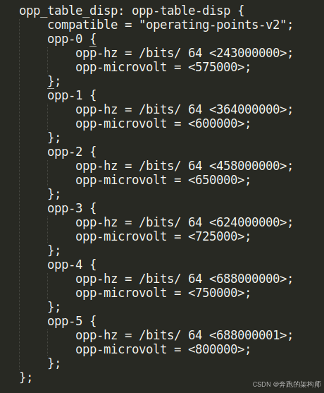
图1-7 Linux OPP Table
事实上,PSCA在SOC的集成手册中已经做好了响应的考虑,如图1-8所示:
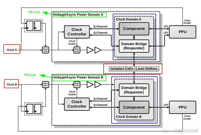
图1-8 Voltage or asynchronous-power domain boundary example
SCP对OSPM传过来的OPP的操作实际上就是对 Clock Domain和Voltage Domain的操作,如果此时PE-Core落在这个两个Domain上,那么就可以完成一次OPP的设置操作。我们对图1-8简化一下,如图1-9所示,也许大家能够更容易理解。
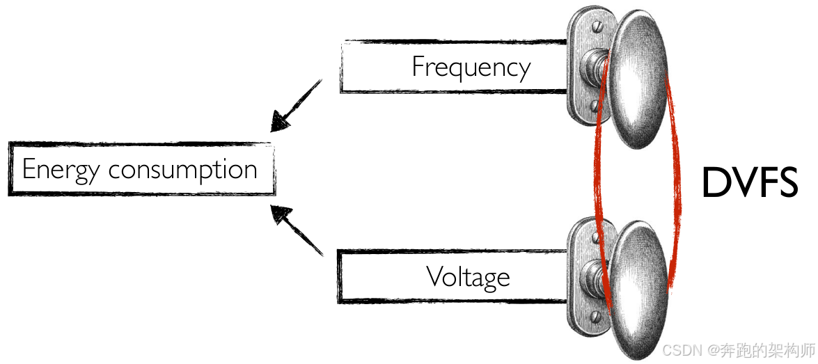
图1-9 DVFS Demo
对主频的调节一定伴随着电压的调节,更高的主频意味着CPU要干更多的事情,也就是需要更多的能量,因此也就需要更高的电压。而更高的电压就意味着更高的功耗,那么就会带来产生更多的热量,对于电子原件来说,热量会改变它们的电气特性,超过限制还可能会造成不可逆的损毁,因此OPP的配置和选择是一个需要反反复复标定的工作。
(3) 那是不是OSPM可以无限制的利用DVFS的机制呢?答案是否定的。不论OSPM下发任何的OPP,SCP都会根据它掌握的系统的状态再做一次决策然后才能决定下一步的动作,这里面要考虑的最重要的因素就是Thermal,目的就是为了保护硬件资源不会因为OSPM强烈的Performance需求而损坏。这个监控的工作通常有SMCF完成,如图1-10所示:
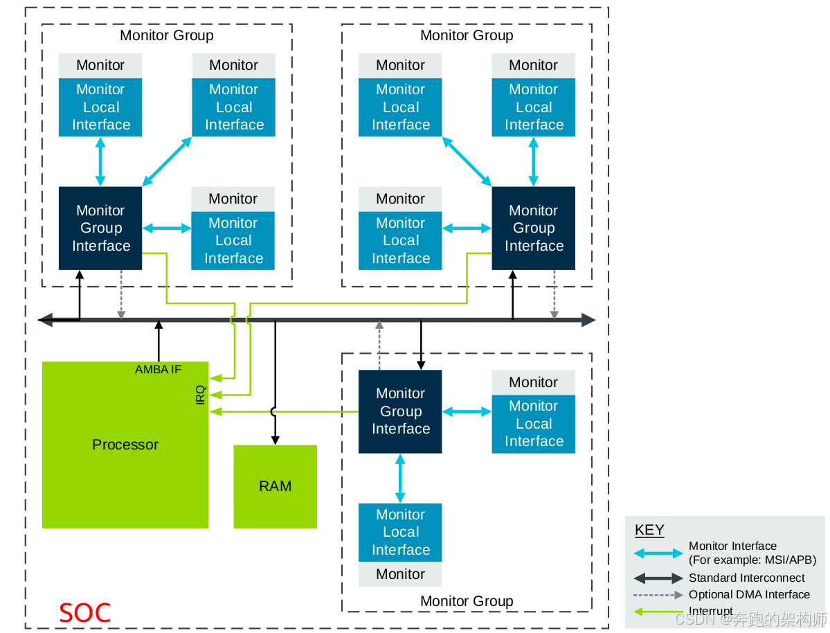
图1-10 System Monitor Control Framework overview
关于SMCF这里我们不展开讨论了,感兴趣的小伙伴可以参考相关手册,这里我们节选部分手册的内容如下:
The System Monitoring Control Framework is designed to manage a large and diverse set of on-chip sensors and monitors. It does this by presenting software with a standard interface to control the monitors, regardless of type, and reducing software load of controlling the monitor sampling and data collection.
The SMCF reduces the burden on monitor control by enabling sampling on multiple monitors to be controlled together and by various triggers either internal or external to the SMCF. The number of monitors that the SMCF supports can be configured.
The SMCF eases data collection requirements by allowing the data from multiple monitors to be collated in a single location or writing out data to a memory-mapped location that is easier for the monitoring agent to access.
The SMCF can also reduce the requirement on the monitoring agent to constantly monitor data by providing programmable alerts that can inform the monitoring agent when certain changes happen, or thresholds are crossed.
The monitoring agent is only required to perform an initial setup and then process data when required on a constant basis or when an alert informs it that analysis or action is required.
The structure of the SMCF is one of distributed monitor groups located around the system where monitoring is required, reusing existing interconnect infrastructure where applicable to communicate.
1.3 DVFS与GPU
上面我们介绍DVFS的操作对象主要是以PE-Core为主,其实总线上的其他IP也可以支持DVFS:
A primary motivation for additional voltage domains is to support DVFS for functional areas of the SoC. DVFS is a fundamental technique for both energy and performance optimization. While initially used for AP cores, it is increasingly being applied to other components of the SoC.
Graphics processing performance in mobile applications has grown significantly and is anticipated to continue. GPU workloads represent throughput processing, with very high inherent parallelism, and are well suited to using DVFS to adapt the performance and energy profile of a given hardware configuration to a frame level deadline.
These properties also enable adaptation to different requirements. Cost-centric designs can implement fewer cores at higher frequency and voltage, while energy-performance-centric designs can implement more cores at lower frequency and voltage.
Therefore, a dedicated voltage domain to enable GPU DVFS is often implemented to enable these benefits.
In applications where DVFS is not required, or the cost is considered to outweigh the benefit, then the GPU cluster is in the V SYS domain.
这里我们举一个具体的例子帮助大家理解手册中关于Graphic芯片支持DVFS,比如MALI-GPU:
GPU utilization counters provide an alternative view of the data path activity cycles, normalizing the queue usage against the total GPU active cycle count. These metrics provide a clearer view of breakdown by workload type, and the effectiveness of queue scheduling.
Mobile systems improve energy efficiency by using Dynamic Voltage and Frequency Scaling (DVFS) to reduce voltage and clock frequency for light workloads. When seeing a workload with high percentage utilization, check the GPU active cycles counter to confirm the frequency. A highly utilized GPU might look like a problem, but it can be caused by a light workload running at a low clock frequency.
A shader core consists of multiple parallel processing units. Performance counters can track utilization and workload characteristics for all the major processing units, allowing developers to find both bottlenecks and content inefficiencies to optimize.
For shader-bound content, the functional unit with the highest loading is likely to be the bottleneck. To improve performance, you can reduce the number of operations of that type in the shader. Alternatively, reduce the precision of the operations to use 8 and 16-bit types so that multiple operations are performed in parallel.
For thermally bound content, reducing the critical path load gives the biggest gain as it allows use of a lower operating frequency. However, reducing load on any functional unit helps improve energy efficiency.
这部分不展开讨论了,核心的观点就是GPU的工作场景随着SOC的迭代对算力的消耗越来越大了,考虑到用户的体验,对于能效的控制也变得非常的重要,因此引入DVFS技术也是推高能效的必要手段。只是GPU和CPU的内核微架构还是有显著区别的,这里我们贴一张MALI的GPU-Core,方便大家做对比研究,如图1-11所示:
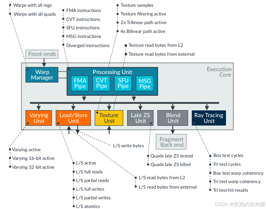
图1-11 Valhall GPU shader core
1.4 DVFS的系统架构
有了前面的铺垫,我们来汇总一下DVFS的系统架构,如图1-12所示:
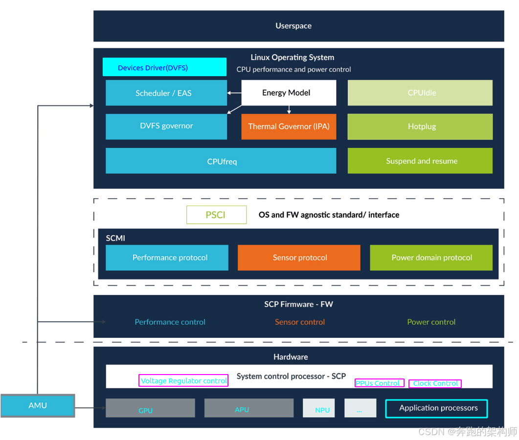
图1-12 DVFS System ARCH
结合上图,我们对DVFS的系统架构总结如下:
(1) 从软件层面,DVFS的管理策略可以工作在PSCA体系下的任何一个Agent上,但是多数情况下只有对功耗需要精细化管控的Agent才会应用DVFS策略。这些应用DVFS策略的大头都在CPU这个节点上,总线上的其他IP如GPU根据配置也可以使用DVFS策略进行能耗管控,但是通常这些策略不会在DVFS内部做出决策而是托管在运行于CPU上的设备驱动中,显然CPU知道的信息更多更容易根据用户的意图做出正确的抉择。比如,用户在CPU上拉起了一个3D应用,那么此时就需要GPU迅速的拉高主频。
(2) 在软件层面DVFS不能割裂的单独工作,通常OSPM会有一整套Energy Model去预测和管理整个OS内部的能效(energy-efficient)。这个EM是OSPM管控整个SOC电源子系统的大脑,一方面它要收集来自系统Sensor的数据,一方面又要考虑到系统内部各个TASK的负载,最后通过CPU的Power代理模块或者是设备的驱动程序将决策后的电源策略通过SCP发送到硬件,比如OPP。
(3) PSCA的框架中已经提供了足够的基础设施帮助OSPM完成DVFS的操作,比如Regulator、Clock、 PPUs等接口,核心的控制节点还是SCP。作为连接OSPM和硬件的纽带,我们需要考虑一个问题那就是如何准确无误的将OSPM的意图传达到总线上的各个IP,还要考虑一个问题就是如何能够降低维护的成本,方便SOC的持续迭代。ARM给出了一个好办法那就是标准化ARM SOC的开发流程,针对DVFS这一块则通过SCMI机制来解决上面这些问题,针对这个机制后面我们会继续讨论。
结语
本文我们从SCP的职能中关于电压和时钟控制开始,逐步展开到PE-Core支持DVFS操作的基础设施(电源域与时钟域),又通过介绍OPP机制延展了一下DVFS工作的核心原理。随后介绍了除了CPU之外,其他总线IP对于DVFS机制支持的情况,比如Graphic芯片目前都需要支持DVFS才能够达到提供能效的目的。最后依托Linux系统从PSCA框架中抽离除了DVFS工作时候的系统架构。电源管理和系统的性能一直都密不可分的,而DVFS又是性能优化的基石,希望通过本文的介绍能够帮助大家打开研究性能优化的大门。今天就到这里,谢谢大家,请关注、转发、评论。
Reference
01 <DEN0050D_Power_Control_System_Architecture.pdf>
02 <armv8_a_power_management_100960_0100_en.pdf>
03 <Power_Policy_Unit_Architecture_Specification_0051E.pdf>
04 <DEN0024A_v8_architecture_PG.pdf>
05 <79-LX-LD-s003-Linux设备驱动开发详解4_0内核-3rd.pdf>
06 <80-PGxxx-35_QNX_Thermal_Manager_Overview.pdf>
07 <80-pgxxx-7_n_qnx_power_management_software_architecture_reference_manual.pdf>
08 <80-ARM-POWER-HK0001_一文搞懂ARM_SoC功耗控制架构.pdf>
09 <Arm_Power_and_Performance_Management_SCMI_White_Paper.pdf>
10 <80-ARM-POWER-cs0001_Arm-SoC-power功耗控制架构.pdf>
11 <80-LX-LK-cl0009_深入理解Linux电源管理.pdf>
12 <DEN0056D_System_Control_and_Management_Interface_v3_1.pdf>
13 <arm_total_compute_2021_reference_design_software_developer_guide_en.pdf>
14 <arm_total_compute_2022_reference_design_software_developer_guide_en.pdf>
15 <arm_cortex_m85_processor_trm_en.pdf>
16 <DEN0108_00eac0_smcf-archl-Specification.pdf>
17 <DEN0022F.b_Power_State_Coordination_Interface.pdf>
18 <MTxxxx_SCP_User_Manual_V1.0.pdf>
19 <learn_the_architecture_arm_system_architectures_en.pdf>
20 <arm_dsu_110_trm_101381_0400_11_en.pdf>
21 <DEN0077A_Firmware_Framework_Arm_A_profile_1.1_EAC0.pdf>
22 <80-LX-POWER-PSCI-cs0001_Linux-PSCI框架.pdf>
23 <learn_the_architecture_realm_management_extension_guide.pdf>
24 <ISA_A64_xml_A_profile-2024-03.pdf>
25 <learn_the_architecture_aarch64_memory_management_guide.pdf>
26 <IHI0069H_gic_architecture_specification.pdf>
27 <DEN0044H_ArmBBR_2.1Final.pdf>
28 <LVC20-118-0-SCMI-server-in-TEE.pdf>
29 <trustedfirmware-a-readthedocs-io-en-latest.pdf>
30 <arm_mali_g615_performance_counters_reference_guide.pdf>
Glossary
AP - application processor
OSPM - Operating System Power Management
WFI - Wait For Interrupt
WFE - Wait For Event
DVFS - Dynamic Voltage and Frequency Scaling
SCU - Snoop Control Unit
OPP - Operating Performance Point
PSCI - Power State Coordination Interface
PPU - Power Policy Unit
PCSA - Power Control System Architecture
SoC - System-on-Chip
PCF - Power Control Framework
SCP - System Control Processor
BSP - board support package
SCMI - System Control and Management Interface
EAS - Energy Aware Scheduling
IPA - Intelligent Power Allocation
ACPI - Advanced Configuration and Power Interface
LPI - Low-Power Idle
CPPC - Collaborative Processor Performance Control
PCSM - power control state machine
AOSS - Always-on subsystem
PMIC - Power Management Integrated Circuit
JM - job manager
AON - always on domain
SBSA - Server Base System Architecture
CLK_CTRL - Clock Controller
LPD - Low Power Distributor
LPC - Low Power Combiner
P2Q - P-Channel to Q-Channel Convertor
GPIO - General Purpose IO
RAS - Reliability, Availability, and Serviceability
STR - Suspend to RAM
SMCCC - SMC Calling Convention
RMM - Realm Management Monitor
BMC - board management controller
PPF - Privileged platform firmwarever
SPM - Secure Partition Manager
SP - Secure Partition
DCVS - Dynamic Clock and Voltage Scaling
V-BSA - Virtual Base System Architecture
BBR - Base Boot Requirements