首先是参考了上述博文的有关iic时序的讲解。
下面是根据正点原子的iic驱动模块的程序结合自己的理解画的时序图,程序中有些计数器对应的时序省略掉了,下面的时序图予以补全。
 其次是状态转移图:
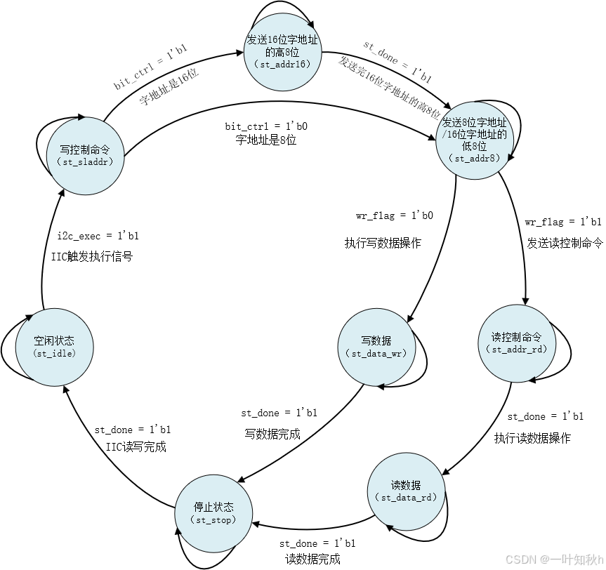
其中需要注意的是,当状态机当前状态处于st_data_rd,也就是从机逐位从sda线上读取数据(输入模式)时,是不需要等待从机的ack应答信号的。
以下是组合逻辑对应的状态转换的程序:
/组合逻辑判断状态转移:
//always@(posedge dri_clk or negedge rst_n)为时序逻辑的判断条件
always@(*)
  begin
    next_state = st_idle;
    case(cur_state)
      st_idle :
        begin
          if(iic_exec)
            next_state <= st_sladdr;
          else
            next_state <= st_idle;
        end
      st_sladdr :
        begin
          if(st_done)
            begin
              if(bit_ctrl)
                next_state <= st_addr16;
            else
                next_state <= st_addr8;
            end
          else
            next_state <= st_sladdr;
        end
      st_addr16 :
        begin
          if(st_done)
            next_state <= st_addr8;
          else
            next_state <= st_addr16;
        end
      st_addr8 :
        begin
          if(st_done)
            begin
              if(wr_flag)
                next_state <= st_addr_rd;
              else
                next_state <= st_addr8;
            end
          else
            next_state <=st_data_wr;
        end
        st_data_wr :
          begin
            if(st_done)
              next_state <= st_stop;
            else
              next_state <= st_data_wr;
          end
        st_addr_rd :
          begin
            if(st_done)
              next_state <= st_data_rd;
            else
              next_state <= st_addr_rd;
          end
        st_data_rd :
          begin
            if(st_done)
              next_state <= st_stop;
            else
              next_state <= st_data_rd;
          end
        st_stop :
          begin
            if(st_done)
              next_state <= st_idle;
            else
              next_state <= st_stop;
          end
        default : next_state= st_idle;
    endcase
  end
再次是时钟分频的过程:
因为iic时钟有三种模式,对应的频率分别魏为:mode1:100k;mode2:400k;mode3:3.4M
一般取mode2快速模式对应的频率,但zynq板载一般为50M时钟,所以需要分频供iic驱动,再者为保证sda输出的数据可以刚好在scl对应的高电平的中间时刻,需要对应的驱动iic的时钟为scl时钟频率的四倍左右。
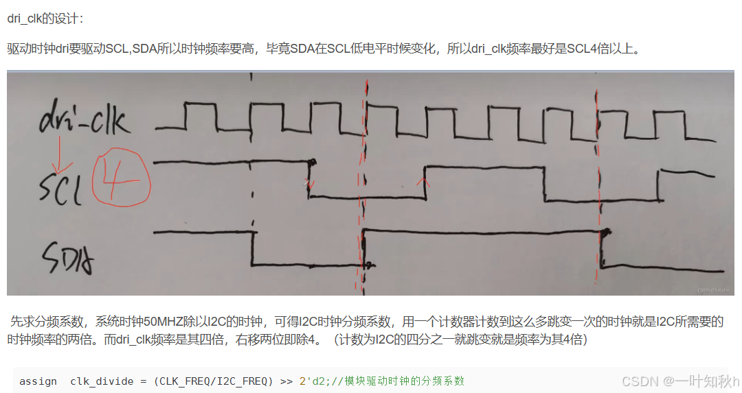
以下是分频部分对应的程序:
//右移两位表示除以4,模块驱动时钟的分频系数(200->50)
assign  clk_divide = (clk_freq/iic_freq) >> 2'd2;

//(clk_divide[8:1])此时是25,因为需要的是50倍,所以需要在25时候翻转
always@(posedge clk or negedge rst_n)
  begin
    if(!rst_n)
    begin
      dri_clk <= 1'b0 ;
      clk_cnt <= 10'b0; //分频时钟计数器
    end
    else if(clk_cnt == ((clk_divide[8:1])-9'd1)
      begin
        clk_cnt <= 10'b0;
        dri_clk = ~ dri_clk;
      end
    else
      clk_cnt = clk_cnt + 10'b1;
  end
最后放上全部的程序:
module iic_dri
#(
parameter slave_addr = 7'b10100000,
parameter clk_freq = 26'd50_000_000,
//mode1:100k;mode2:400k;mode3:3.4M
parameter iic_freq = 18'd250_000
)
(
input clk ,
input rst_n ,
input iic_exec, //触发执行信号
input bit_ctrl, //8/16字节控制位
input iic_rh_wl, //读写控制位read(1) write(0)
input [15:0] iic_addr, //器件内地址
input [7:0] iic_data_w, //写入的数据
output [7:0] iic_data_r, //读出的数据 (从机发给主机的数据)
output reg iic_done,
output reg iic_ack, //应答位,0表示正确应答
output reg scl,
inout sda,
output reg dri_clk //驱动I2C操作的驱动时钟
//驱动iic_scl的时钟频率一般是scl时钟的4倍
);
//状态机切换,各种状态定义
localparam st_idle = 8'b0000_0001; //空闲状态
localparam st_sladdr = 8'b0000_0010; //发送器件地址(slave address)
localparam st_addr16 = 8'b0000_0100; //发送16位字地址
localparam st_addr8 = 8'b0000_1000; //发送8位字地址
localparam st_data_wr = 8'b0001_0000; //写数据(8 bit)
localparam st_addr_rd = 8'b0010_0000; //发送器件地址读
localparam st_data_rd = 8'b0100_0000; //读数据(8 bit)
localparam st_stop = 8'b1000_0000; //结束I2C操作
//在I2C通信中,SDA线的方向需要根据通信状态动态切换。
//写操作时,SDA线配置为输出模式;读操作时,SDA线配置为输入模式。
reg sda_dir ; //I2C数据(SDA)方向控制
reg sda_out ; //SDA输出信号
reg st_done ; //状态结束
reg wr_flag ; //写标志
reg [ 6:0] cnt ; //计数
reg [ 7:0] cur_state ; //状态机当前状态
reg [ 7:0] next_state; //状态机下一状态
reg [15:0] addr_t ; //器件内寄存器地址
reg [ 7:0] data_r ; //读取的数据
reg [ 7:0] data_wr_t ; //I2C需写的数据的临时寄存
reg [ 9:0] clk_cnt ; //分频时钟计数
//wire define
wire sda_in ; //SDA输入信号(数据)
wire [8:0] clk_divide ; //模块驱动时钟的分频系数
//(sda_dir,是判断条件,确定sda是输出还是输入模式)
assign sda = sda_dir ? sda_out : 1'bz;
assign sda_in = sda ; //SDA数据输入(主设备释放总线后)
assign clk_divide = (clk_freq/iic_freq) >> 2'd2;//模块驱动时钟的分频系数(200->50)
//(clk_divide[8:1])此时是25,因为需要的是50倍,所以需要在25时候翻转
always@(posedge clk or negedge rst_n)
begin
if(!rst_n)
begin
dri_clk <= 1'b0 ;
clk_cnt <= 10'b0; //分频时钟计数器
end
else if(clk_cnt == ((clk_divide[8:1])-9'd1)
begin
clk_cnt <= 10'b0;
dri_clk = ~ dri_clk;
end
else
clk_cnt = clk_cnt + 10'b1;
end
//状态转换 同步时钟
always@(posedge dri_clk or negedge rst_n)
begin
if(!rst_n)
cur_state <= st_idle;
else
cur_state <= next_state;
end
//组合逻辑判断状态转移:
//always@(posedge dri_clk or negedge rst_n)为时序逻辑的判断条件
always@(*)
begin
next_state = st_idle;
case(cur_state)
st_idle :
begin
if(iic_exec)
next_state <= st_sladdr;
else
next_state <= st_idle;
end
st_sladdr :
begin
if(st_done)
begin
if(bit_ctrl)
next_state <= st_addr16;
else
next_state <= st_addr8;
end
else
next_state <= st_sladdr;
end
st_addr16 :
begin
if(st_done)
next_state <= st_addr8;
else
next_state <= st_addr16;
end
st_addr8 :
begin
if(st_done)
begin
if(wr_flag)
next_state <= st_addr_rd;
else
next_state <= st_addr8;
end
else
next_state <=st_data_wr;
end
st_data_wr :
begin
if(st_done)
next_state <= st_stop;
else
next_state <= st_data_wr;
end
st_addr_rd :
begin
if(st_done)
next_state <= st_data_rd;
else
next_state <= st_addr_rd;
end
st_data_rd :
begin
if(st_done)
next_state <= st_stop;
else
next_state <= st_data_rd;
end
st_stop :
begin
if(st_done)
next_state <= st_idle;
else
next_state <= st_stop;
end
default : next_state= st_idle;
endcase
end
//时序逻辑表示状态输出:
always@(posedge dri_clk or negedge rst_n)
begin
if(!rst_n)
begin
sda_dir <= 1'b1;
sda_out <= 1'b1;
scl <= 1'b1;
iic_done <= 1'b0;
iic_data_r <= 1'b0;
iic_ack <= 1'b0;
st_done <= 1'b0;
cnt <= 1'b0;
addr_t <= 1'b0;//初始化为 0,表示尚未设置目标地址。在 I2C 写操作中,目标地址会存储到 addr_t。
data_r <= 1'b0;
data_wr_t <= 1'b0;
wr_flag <= 1'b0;//read(1) write(0),读写判断
end
else
begin
//状态切换和计数器除了在特定状态被打断其他时刻都在切换和计数
st_done <= 1'b0 ;
cnt <= cnt + 7'b1 ;
case(cur_state)
st_idle :
begin
sda_dir <= 1'b1;
sda_out <= 1'b1;
scl <= 1'b1;
i2c_done<= 1'b0;
cnt <= 7'b0;
if(iic_exec)
begin
wr_flag <= iic_rh_wl;
addr_t <= iic_addr;//器件内地址的寄存器
data_wr_t <=iic_data_w;
end
end
st_sladdr :
begin
case(cnt)
7'd1 : sda_out <=1'b0;
//7'd2 : sda_out <=1'b0;
7'd3 : scl <=1'b0;//scl,高时,sda,由高变低(start)
7'd4 : sda_out <=SLAVE_ADDR[6];
//7'd5 : scl <=1'b0;
7'd6 : scl <=1'b1;
7'd7 : scl <=1'b0;
7'd8 : sda_out <=SLAVE_ADDR[5];
7'd9 : scl <=1'b1;
//7'd10 : scl <=1'b1;
7'd11 : scl <=1'b0;
7'd12 : sda_out<=SLAVE_ADDR[4];
7'd13 : scl <=1'b1;
//7'd14 : scl <=1'b1;
7'd15 : scl <=1'b0;
7'd16 : sda_out<=SLAVE_ADDR[3];
7'd17 : scl <=1'b1;
//7'd18 : scl <=1'b1;
7'd19 : scl <=1'b0;
7'd20 : sda_out<=SLAVE_ADDR[2];
7'd21 : scl <=1'b1;
//7'd22 : scl <=1'b1;
7'd23 : scl <=1'b0;
7'd24 : sda_out<=SLAVE_ADDR[1];
7'd25 : scl <=1'b1;s
//7'd26 : scl <=1'b1;
7'd27 : scl <=1'b0;
7'd28 : sda_out<=SLAVE_ADDR[0];
7'd29 : scl <=1'b1;
//7'd30 : scl <=1'b1;
7'd31 : scl <=1'b0;
7'd32 : sda_out<=1'b0; //0:写
7'd33 : scl <=1'b1; //此时写操作标志失效 r/w 读写控制位
//7'd34 : scl <=1'b1;
7'd35 : scl <=1'b0;
7'd36 :
sda_dir <= 1'b0; //将 SDA 设置为输入模式
sda_out <= 1'b1; //释放总线
7'd37 : scl <=1'b1; //此时从机可以在scl高电平发送信号
7'd38 :
begin
st_done <= 1'b1;
if(sda_in == 1'b1) //高电平表示从机未应答
iic_ack <=1'b1;
end
7'd39 :
begin
scl <=1'b0;
cnt <=7'd0;
end
default: ; //无默认值,表示空操作
endcase
end
//sda_dir 为高电平时为输出模式,主设备控制,为低电平时为输入模式
st_addr16:
begin
case(cnt)
7'd0 :
begin
sda_dir <= 1'b1 ;
sda_out <= addr_t[15]; //传送字地址
end
//在 I2C 通信中,scl 是时钟线,用于同步数据的传输。
//每个数据位的传输都需要一个完整的时钟周期,
//即 scl 从低电平到高电平再回到低电平的过程。
7'b1 : scl <=1'b1;
//7'd2 : scl <=1'b1;
7'd3 : scl <=1'b0;
7'd4 : sda_out <=addr_t[14];
7'd5 : scl <=1'b1;
//7'd6 : scl <=1'b1;
7'd7 : scl <=1'b0;
7'd8 : sda_out <=addr_t[13];
7'd9 : scl <=1'b1;
//7'd10 : scl <=1'b1;
7'd11 : scl <=1'b0;
7'd12 : sda_out <=addr_t[12];
7'd13 : scl <=1'b1;
//7'd14 : scl <=1'b1;
7'd15 : scl <=1'b0;
7'd16 : sda_out <=addr_t[11];
7'd17 : scl <=1'b1;
7'd18 : scl <=1'b1;
7'd19 : scl <=1'b0;
7'd20 : sda_out <=addr_t[10];
7'd21 : scl <=1'b1;
//7'd22 : scl <=1'b1;
7'd23 : scl <=1'b0;
7'd24 : sda_out <=addr_t[9];
7'd25 : scl <=1'b1;
//7'd26 : scl <=1'b1;
7'd27 : scl <=1'b0;
7'd28 : sda_out <=addr_t[8];
7'd29 : scl <=1'b1;
//7'd30 : scl <=1'b1;
7'd31 : scl <=1'b0; //在scl结束一个周期之后
7'd32 :
begin
sda_dir <= 1'b0; //释放总线,等待从设备应答信号
sda_out <= 1'b1; //上拉,避免主从设备通信冲突
end
7'd33 : scl <=1'b1;
7'd34 :
begin
st_done <=1'b1;
if(sda_in == 1'b1) //高电平表示从机未应答
iic_ack <=1'b1;
end
7'd35 :
begin
scl <=1'b0;
cnt <=1'b0;
end
default : ;
endcase
end
st_addr8 :
begin
case(cnt)
7'd0 :
begin
sda_dir <=1'b1;//将总线设为输出模式
sda_out <=addr_t[7];//保证在sdl被拉高时可以稳定传输
end
7'd1 :scl <= 1'b1;
//7'd2 :scl <= 1'b1;
7'd3 :scl <= 1'b0;
7'd4 :sda_out <= addr_t[6];
7'd5 :scl <= 1'b1;
//7'd6 :scl <= 1'b1;
7'd7 :scl <= 1'b0;
7'd8 :sda_out <= addr_t[5];
7'd9 :scl <= 1'b1;
//7'd10 :scl <= 1'b1;
7'd11 :scl <= 1'b0;
7'd12 :sda_out <= addr_t[4];
7'd13 :scl <= 1'b1;
//7'd14 :scl <= 1'b1;
7'd15 :scl <= 1'b0;
7'd16 :sda_out <= addr_t[3];
7'd17 :scl <= 1'b1;
//7'd18 :scl <= 1'b1;
7'd19 :scl <= 1'b0;
7'd20 :sda_out <= addr_t[2];
7'd21 :scl <= 1'b1;
//7'd22 :scl <= 1'b1;
7'd23 :scl <= 1'b0;
7'd24 :sda_out <= addr_t[1];
7'd25 :scl <= 1'b1;
//7'd26 :scl <= 1'b1;
7'd27 :scl <= 1'b0;
7'd28 :sda_out <= addr_t[0];
7'd29 :scl <= 1'b1;
//7'd30 :scl <= 1'b1;
7'd31 :scl <= 1'b0;//在scl结束一个周期之后
7'd32 :
begin
sda_dir <=1'b0;
sda_out <=1'b1;
end
7'd33 :scl <= 1'b1;
7'd34 :
begin
st_done <=1'b1;
if(sda_in == 1'b1)//从机正常应答会将sda总线拉低
iic_ack <= 1'b1;//高电平表示从机未应答
end
7'd35 :
begin
scl <= 1'b0;
cnt <= 1'b0;
end
default : ;
endcase
end
//写数据需要主设备控制sda线,也就需要设为输出模式
st_data_wr :
begin
case(cnt)
7'd0 :
begin
sda_dir <=1'b1;
sda_out <=data_wr_t[7];
end
7'd1 : scl <=1'b1;
//7'd2 : scl <=1'b1;
7'd3 : scl <=1'b0;
7'd4 : sda_out <=data_wr_t[6];
7'd5 : scl <=1'b1;
//7'd6 : scl <=1'b1;
7'd7 : scl <=1'b0;
7'd8 : sda_out <=data_wr_t[5];
7'd9 : scl <=1'b1;
//7'd10 : scl <=1'b1;
7'd11 : scl <=1'b0;
7'd12 : sda_out <=data_wr_t[4];
7'd13 : scl <=1'b1;
//7'd14 : scl <=1'b1;
7'd15 : scl <=1'b0;
7'd16 : sda_out <=data_wr_t[3];
7'd17 : scl <=1'b1;
//7'd18 : scl <=1'b1;
7'd19 : scl <=1'b0;
7'd20 : sda_out <=data_wr_t[2];
7'd21 : scl <=1'b1;
//7'd22 : scl <=1'b1;
7'd23 : scl <=1'b0;
7'd24 : sda_out <=data_wr_t[1];
7'd25 : scl <=1'b1;
//7'd26 : scl <=1'b1;
7'd27 : scl <=1'b0;
7'd28 : sda_out <=data_wr_t[0];
7'd29 : scl <=1'b1;
//7'd30 : scl <=1'b1;
7'd31 : scl <=1'b0;
7'd32 :
begin
sda_dir <= 1'b0;
sda_out <= 1'b1;//释放总线,拉高sda等待从机应答
end
7'd33 : scl <=1'b1; //需要确定在scl高电平时采样,等待从机应答信号
7'd34 :
begin
st_done <= 1'b1;
if(sda_in == 1'b1)
iic_ack <=1'b1;
end
7'd35 :
begin
scl <=1'b0;
cnt <=1'b0;
end
default : ;
endcase
end
st_addr_rd :
begin
case(cnt)
7'd1 : scl <=1'b1;
//7'd2 : scl <=1'b1;
7'd3 : scl <=1'b0;
7'd4 : sda_out <=SLAVE_ADDR[6];
7'd5 : scl <=1'b1;
//7'd6 : scl <=1'b1;
7'd7 : scl <=1'b0;
7'd8 : sda_out <=SLAVE_ADDR[5];
7'd9 : scl <=1'b1;
//7'd10 : scl <=1'b1;
7'd11 : scl <=1'b0;
7'd12 : sda_out <=SLAVE_ADDR[4];
7'd13 : scl <=1'b1;
//7'd14 : scl <=1'b1;
7'd15 : scl <=1'b0;
7'd16 : sda_out <=SLAVE_ADDR[3];
7'd17 : scl <=1'b1;
//7'd18 : scl <=1'b1;
7'd19 : scl <=1'b0;
7'd20 : sda_out <=SLAVE_ADDR[2];
7'd21 : scl <=1'b1;
//7'd22 : scl <=1'b1;
7'd23 : scl <=1'b0;
7'd24 : sda_out <=SLAVE_ADDR[1];
7'd25 : scl <=1'b1;
//7'd26 : scl <=1'b1;
7'd27 : scl <=1'b0;
7'd28 : sda_out <=SLAVE_ADDR[0];
7'd29 : scl <=1'b1;
//7'd30 : scl <=1'b1;
7'd31 : scl <=1'b0;
7'd32 : sda_out <=1'b1;//主机控制,输出模式,读从机发的地址
7'd33 : scl <=1'b1;
//7'd34 : scl <=1'b1;
7'd35 : scl <=1'b0;
7'd36 :
begin
sda_dir <= 1'b0;
sda_out <= 1'b1;
end
7'd37 : scl <=1'b1;
7'd38 :
begin
st_done <= 1'b1;
if(sda_in == 1'b1) //sda,释放总线后等待从机应答信号
iic_ack <= 1'b1;
end
7'd39 :
begin
scl <= 1'b0;
cnt <= 1'b0;
end
default : ;
endcase
end
st_data_rd :
begin
case(cnt)
//data_r,用于逐位从sda线上读取数据
7'd0 : sda_dir <= 1'b0; //从机控制在scl,上升沿写入数据到sda
7'd1 :
begin
data_r[7] <=sda_in;
scl <=1'b1;
end
7'd2 : scl <=1'b1;
7'd3 : scl <=1'b0;
7'd4 : sda_out <=SLAVE_ADDR[6];
7'd5 :
begin
data_r[6] <=sda_in;
scl <=1'b1;
end
7'd6 : scl <=1'b1;
7'd7 : scl <=1'b0;
7'd8 : sda_out <=SLAVE_ADDR[5];
7'd9 :
begin
data_r[5] <=sda_in;
scl <=1'b1;
end
7'd10 : scl <=1'b1;
7'd11 : scl <=1'b0;
7'd12 : sda_out <=SLAVE_ADDR[4];
7'd13 :
begin
data_r[4] <=sda_in;
scl <=1'b1;
end
7'd14 : scl <=1'b1;
7'd15 : scl <=1'b0;
7'd16 : sda_out <=SLAVE_ADDR[3];
7'd17 :
begin
data_r[3] <=sda_in;
scl <=1'b1;
end
7'd18 : scl <=1'b1;
7'd19 : scl <=1'b0;
7'd20 : sda_out <=SLAVE_ADDR[2];
7'd21 :
begin
data_r[2] <=sda_in;
scl <=1'b1;
end
7'd22 : scl <=1'b1;
7'd23 : scl <=1'b0;
7'd24 : sda_out <=SLAVE_ADDR[1];
7'd25 :
begin
data_r[1] <=sda_in;
scl <=1'b1;
end
7'd26 : scl <=1'b1;
7'd27 : scl <=1'b0;
7'd28 : sda_out <=SLAVE_ADDR[0];
7'd29 :
begin
data_r[0] <=sda_in;
scl <=1'b1;
end
7'd30 : scl <=1'b1;
7'd31 : scl <=1'b0;
7'd32 :
begin
sda_dir <= 1'b1; //主机输出模式
sda_out <= 1'b1;
end
7'd33 : scl <=1'b1;//延后一个时刻确保从机在上升沿采样完成,避免主从机产生冲突
7'd34 : st_done <=1'b1;
7'd35 :
begin
scl <=1'b0;
cnt <= 7'b0;
i2c_data_r <= data_r; //将读到的数据发送给主机
end
default : ;
endcase
end
st_stop :
begin
case(cnt)
7'd0 :
begin
scl <=1'b1;
sda_out <= 1'b0;
end
7'd1 : scl <=1'b1;
7'd2 : scl <=1'b1;
7'd3 : sda_out <=1'b1; //stop标志
7'd15 : st_done <= 1'b1;
7'd16 :
begin
cnt <= 7'b0;
i2c_done <= 1'b1;
end
default : ;
endcase
end
endcase
end
end
endmodule 程序中对应的每个状态都有注释讲解, 但还有几个地方需要注意,sda在输入时是在scl的上升沿采样,为了保证sda在scl的每个高电平期间可以稳定的传输数据,而在给sda_out赋值的时候则是需要在scl稳定的低电平期间,也就是时序图中sda_out的上升沿和下降沿切换的时候。