本文参考AXI官方IP源码 和博主FPGA奇哥用verilog成功编写了AXI FULL主机协议,并通过zynq开发板成功将数据写入DDR3中,同时编写了testbench代码,用ILA验证
编写AXI协议作用
1.掌握了AXI协议的编写,由自己编写的AXI协议相比于官方IP更精简,同时对AXI协议理解更深
2.完成了zynq利用pl端读写DDR3(基于zynq7020领航者开发板)
3.模块化编程有了更深一步的理解,同时解决了一个bug,即在自动连线时rlast经过axi_interconnection被拉高的解决方法
首先总体代码如下:
cpp
//作者:CSDN建筑玩家
//AXI FULL MASTER的VERILOG实现,实现与xilinx原版axi协议兼容对接
//时间:2025/11/3

module axi_full_master#(
    //32位基地址
    parameter  C_M_TARGET_SLAVE_BASE_ADDR	= 32'h40000000,
    //突发长度,包含1, 2, 4, 8, 16, 32, 64, 128, 256
    parameter integer C_M_AXI_BURST_LEN	= 16,
    //ID标识宽度定义
    parameter integer C_M_AXI_ID_WIDTH	= 1,
    //地址位宽
    parameter integer C_M_AXI_ADDR_WIDTH	= 32,
    //数据位宽
    parameter integer C_M_AXI_DATA_WIDTH	= 32,
    //写地址时用户自定义信号位宽
    parameter integer C_M_AXI_AWUSER_WIDTH	= 0,
    //写地址时用户自定义信号位宽
    parameter integer C_M_AXI_ARUSER_WIDTH	= 0,
    // Width of User Write Data Bus
	parameter integer C_M_AXI_WUSER_WIDTH	= 0,
	// Width of User Read Data Bus
	parameter integer C_M_AXI_RUSER_WIDTH	= 0,
	// Width of User Response Bus
	parameter integer C_M_AXI_BUSER_WIDTH	= 0
)
(
    //-------全局信号----------//
	input wire  INIT_AXI_TXN    ,//初始触发信号
	output wire  TXN_DONE       ,//发送完成
	output reg  ERROR           ,//发送错误
	input wire  M_AXI_ACLK      ,//时钟
	input wire  M_AXI_ARESETN   ,//复位
    //-------写地址信号--------//
    output wire [C_M_AXI_ID_WIDTH-1 : 0] M_AXI_AWID,//0
    output wire [C_M_AXI_ADDR_WIDTH-1 : 0] M_AXI_AWADDR,//地址
    output wire [7 : 0] M_AXI_AWLEN,//1, 2, 4, 8, 16, 32, 64, 128, 256这几个值减1,使用参数化设计上面的值,然后再减1
    output wire [2 : 0] M_AXI_AWSIZE,//用case语句网表和8/16/32/64/128/256/512/1024一一对应即可,计算方式  (数据宽度/8-1)的位宽
    output wire [1 : 0] M_AXI_AWBURST,//00地址不变,01地址递增,10地址增加到当前突发极限
    output wire  M_AXI_AWLOCK,//0
    output wire [3 : 0] M_AXI_AWCACHE,//4'b1111
    output wire [2 : 0] M_AXI_AWPROT,//0
    output wire [3 : 0] M_AXI_AWQOS,//0
    output wire [C_M_AXI_AWUSER_WIDTH-1 : 0] M_AXI_AWUSER,//0
    output wire  M_AXI_AWVALID,//实现启动信号启动时置1,接收到应答置0
    input wire  M_AXI_AWREADY,//应答
    //-------写数据信号--------//
	output wire [C_M_AXI_DATA_WIDTH-1 : 0] M_AXI_WDATA,
	output wire [C_M_AXI_DATA_WIDTH/8-1 : 0] M_AXI_WSTRB,//这一组表示突发信号的哪些字节有效,例如32位数据都有效,4'b1111
	output wire  M_AXI_WLAST,//一组突发的最后一个信号拉高
	output wire [C_M_AXI_WUSER_WIDTH-1 : 0] M_AXI_WUSER,//无需关心
	output wire  M_AXI_WVALID,
	input wire  M_AXI_WREADY,
    //-------写响应信号--------//
	input wire [C_M_AXI_ID_WIDTH-1 : 0] M_AXI_BID,
	input wire [1 : 0] M_AXI_BRESP,//00应答成功、01独占访问成功、10从机错误(如地址无效)、解码错误(如无从机)
	//input wire [C_M_AXI_BUSER_WIDTH-1 : 0] M_AXI_BUSER,//用户自定义信号,无需关心
	input wire  M_AXI_BVALID,
	output wire  M_AXI_BREADY,
    //-------读地址信号--------//
	output wire [C_M_AXI_ID_WIDTH-1 : 0] M_AXI_ARID,//读数据地址ID,0
	output wire [C_M_AXI_ADDR_WIDTH-1 : 0] M_AXI_ARADDR,//读数据地址
	output wire [7 : 0] M_AXI_ARLEN,//读数据突发长度,1, 2, 4, 8, 16, 32, 64, 128, 256这几个值减1,使用参数化设计上面的值,然后再减1
	output wire [2 : 0] M_AXI_ARSIZE,//读数据宽度,用case语句网表和8/16/32/64/128/256/512/1024一一对应即可
	output wire [1 : 0] M_AXI_ARBURST,//突发类型,01
	output wire  M_AXI_ARLOCK,//0
	output wire [3 : 0] M_AXI_ARCACHE,//4'b1111
	output wire [2 : 0] M_AXI_ARPROT,//0
	output wire [3 : 0] M_AXI_ARQOS,//0
	output wire [C_M_AXI_ARUSER_WIDTH-1 : 0] M_AXI_ARUSER,//0
	output wire  M_AXI_ARVALID,
	input wire  M_AXI_ARREADY,
    //-------读数据信号--------//
	input wire [C_M_AXI_ID_WIDTH-1 : 0] M_AXI_RID,//0
	input wire [C_M_AXI_DATA_WIDTH-1 : 0] M_AXI_RDATA,//数据
	input wire [1 : 0] M_AXI_RRESP,//反映是否出错
	input wire  M_AXI_RLAST,
	input wire [C_M_AXI_RUSER_WIDTH-1 : 0] M_AXI_RUSER,//0,自定义信号,无特别需求
	input wire  M_AXI_RVALID,
	output wire  M_AXI_RREADY
);
    wire rst_n;
    wire clk;
    assign rst_n=M_AXI_ARESETN;
    assign clk=M_AXI_ACLK;
//写地址信号
    reg [C_M_AXI_ADDR_WIDTH-1 : 0] awaddr;
    reg awvalid;
    wire burst_size_bytes;//每次突发地址增加
    assign burst_size_bytes	= C_M_AXI_BURST_LEN * C_M_AXI_DATA_WIDTH/8;
    reg bready,rready;
    reg start_reg1,start_reg2;
    always @(posedge clk) begin
        if(!rst_n)begin
            start_reg1<=0;
            start_reg2<=0;
        end
        else begin
            start_reg1<=INIT_AXI_TXN;
            start_reg2<=start_reg1;
        end
    end
    wire start_flag;
    assign start_flag=start_reg1 & !start_reg2;
    wire wlast;
    assign wlast=(cnt_wdata_nums==C_M_AXI_BURST_LEN-1&&M_AXI_WVALID&&M_AXI_WREADY)?1:0;
    assign write_resp_error = bready & M_AXI_BVALID & M_AXI_BRESP[1];
    assign read_resp_error = rready & M_AXI_RVALID & M_AXI_RRESP[1];
    always @(posedge clk) begin
        if(!rst_n||start_flag)
            ERROR<=0;
        else
            if(write_resp_error||read_resp_error)
                ERROR<=1;
            else
                ERROR<=ERROR;
    end
/*------------------------写地址信号赋值------------------------*/
    assign M_AXI_AWID=1'b0;
    assign M_AXI_AWADDR=C_M_TARGET_SLAVE_BASE_ADDR+awaddr;//基地址加上内部逻辑设计的地址
    assign M_AXI_AWLEN=C_M_AXI_BURST_LEN-1;
    reg [2 : 0] awsize;
    assign M_AXI_AWSIZE=awsize;
    always @(*) begin
        if(!rst_n)
            awsize=0;
        else
        case (C_M_AXI_DATA_WIDTH)
             8:  awsize=3'b000;
             16: awsize=3'b001;
             32: awsize=3'b010;
             64: awsize=3'b011;
             128:awsize=3'b100;
             256:awsize=3'b101;
             512:awsize=3'b110;
             1024:awsize=3'b111;
             default: awsize=3'b010;
         endcase
    end
    assign M_AXI_AWBURST=2'b01;//突发自增,通用性比较强
    assign M_AXI_AWLOCK=1'b0;
    assign M_AXI_AWCACHE=4'b0010;//如果连接ZYNQ ACP,选择0011
    assign M_AXI_AWPROT=0;
    assign M_AXI_AWQOS=0;
    assign M_AXI_AWUSER=0;
    assign M_AXI_AWVALID=awvalid;
    reg write_start;
    reg start_w1,start_w2;
    always @(posedge clk) begin
        if(!rst_n)begin
            start_w1<=0;
            start_w2<=0;
        end
        else begin
            start_w1<=write_start;
            start_w2<=start_w1;
        end
    end
    wire startw_flag;
    assign startw_flag=start_w1 & !start_w2;
    always @(posedge clk) begin
        if(!rst_n)begin
            awvalid<=0;
        end
        else begin
            if(!awvalid&&startw_flag)//上升沿触发
                awvalid<=1;
            else if(awvalid&&M_AXI_AWREADY)
                awvalid<=0;
        end
    end
    always @(posedge clk) begin
        if(!rst_n||start_flag)begin
            awaddr<=0;
        end
        else begin
            if(awvalid&&M_AXI_AWREADY)
                awaddr<=awaddr+C_M_AXI_BURST_LEN*C_M_AXI_DATA_WIDTH/8;
            else
                awaddr<=awaddr;
        end
    end
/*------------------------写数据信号赋值------------------------*/
    reg [C_M_AXI_DATA_WIDTH-1:0] wdata;
    assign M_AXI_WDATA=wdata;
    always @(posedge clk) begin
        if(!rst_n||awvalid&&M_AXI_AWREADY)
            wdata<=1;
        else begin
            if(M_AXI_WVALID&&M_AXI_WREADY)
                wdata<=wdata+1;
            else
                wdata<=wdata;
        end
    end
    assign M_AXI_WSTRB={(C_M_AXI_DATA_WIDTH/8){1'b1}};
    assign M_AXI_WLAST=wlast;
    reg[8:0] cnt_wdata_nums;//每次突发时计数,直到完整的突发发送完毕
    always @(posedge clk) begin
        if(!rst_n||(awvalid&&M_AXI_AWREADY))
            cnt_wdata_nums<=0;
        else begin
            if(cnt_wdata_nums<C_M_AXI_BURST_LEN-1&&M_AXI_WVALID&&M_AXI_WREADY)begin
                cnt_wdata_nums<=cnt_wdata_nums+1;
            end
        end
    end
    assign TXN_DONE=((cnt_wdata_nums==C_M_AXI_BURST_LEN-1)&&M_AXI_WVALID&&M_AXI_WREADY)?1:0;
    assign M_AXI_WUSER=0;
    reg wvalid;
    assign M_AXI_WVALID=wvalid;
    always @(posedge clk) begin
        if(!rst_n)
            wvalid<=0;
        else begin
            if(awvalid&&M_AXI_AWREADY)
                wvalid<=1;
            else if(wlast)
                wvalid<=0;
        end
    end
/*------------------------写响应信号赋值------------------------*/
    assign M_AXI_BREADY=bready;
    always @(posedge clk) begin
        if(!rst_n)
            bready<=0;
        else begin
            if(awvalid&&M_AXI_AWREADY)
                bready<=1;
            else if(bready&&M_AXI_BVALID)
                bready<=0;
        end
    end
    reg [1 : 0] bresp;
    always @(posedge clk) begin
        if(!rst_n||awvalid&&M_AXI_AWREADY)
            bresp<=0;
        else
            if(bready&&M_AXI_BVALID)
                bresp<=M_AXI_BRESP;
    end
/*------------------------读地址信号赋值------------------------*/
    assign M_AXI_ARID=1'b0;
    reg [C_M_AXI_ADDR_WIDTH-1 : 0] araddr;
    wire rlast;
    assign rlast=M_AXI_RLAST;
    assign M_AXI_ARADDR=C_M_TARGET_SLAVE_BASE_ADDR+araddr;
    always @(posedge clk) begin
        if(!rst_n||start_flag)
            araddr<=0;
        else begin
            if(rlast&&M_AXI_RREADY&&M_AXI_RVALID)
                araddr<=araddr+C_M_AXI_BURST_LEN*C_M_AXI_DATA_WIDTH/8;
        end
    end
    assign M_AXI_ARLEN=C_M_AXI_BURST_LEN-1;
    reg [2 : 0] arsize;
    assign M_AXI_ARSIZE=arsize;
    always @(*) begin
        if(!rst_n)
            arsize=0;
        else
        case (C_M_AXI_DATA_WIDTH)
             8:  arsize=3'b000;
             16: arsize=3'b001;
             32: arsize=3'b010;
             64: arsize=3'b011;
             128:arsize=3'b100;
             256:arsize=3'b101;
             512:arsize=3'b110;
             1024:arsize=3'b111;
             default: arsize=3'b010;
         endcase
    end
    assign M_AXI_ARBURST=2'b01;
    assign M_AXI_ARLOCK=0;
    assign M_AXI_ARCACHE=4'b1111;
    assign M_AXI_ARPROT=0;
    assign M_AXI_ARQOS=0;
    assign M_AXI_ARUSER=0;
    reg read_start;//一次完整读突发启动
    reg start_r1,start_r2;
    always @(posedge clk) begin
        if(!rst_n)begin
            start_r1<=0;
            start_r2<=0;
        end
        else begin
            start_r1<=read_start;
            start_r2<=start_r1;
        end
    end
    wire startr_flag;
    assign startr_flag=start_r1 & !start_r2;
    reg arvalid;
    always @(posedge clk) begin
        if(!rst_n)
            arvalid<=0;
        else begin
            if(!arvalid&&startr_flag)
                arvalid<=1;
            else if(arvalid&&M_AXI_ARREADY)
                arvalid<=0;
        end
    end
    assign M_AXI_ARVALID=arvalid;
/*------------------------读数据信号赋值------------------------*/
    reg [C_M_AXI_DATA_WIDTH-1 : 0] rdata_reg;
    reg rvalid;
    assign M_AXI_RREADY=rready;
    always @(posedge clk) begin
        if(!rst_n)
            rready<=0;
        else begin
            if(arvalid&&M_AXI_ARREADY)
                rready<=1;
            else if(M_AXI_RLAST&&M_AXI_RVALID&&M_AXI_RREADY)
                rready<=0;
        end
    end
/*------------------------状态机设计------------------------*/
//目的,先写一组突发,再读一组突发

reg [2:0] cur_state,next_state;
parameter IDLE = 3'b000,
          WDATA= 3'b001,
          RDATA= 3'b010;

    always @(posedge clk) begin
        if(!rst_n)
            cur_state<=IDLE;
        else
            cur_state<=next_state;
    end
    always @(*) begin
        if(!rst_n)
            next_state<=IDLE;
        else begin
            case (cur_state)
            IDLE :begin
                if(start_flag)
                    next_state<=WDATA;
                else
                    next_state<=IDLE;
            end
            WDATA:begin
                if(wlast)
                    next_state<=RDATA;
                else
                    next_state<=WDATA;
            end
            RDATA:begin
                if(rlast&&M_AXI_RVALID&&M_AXI_RREADY)
                    next_state<=IDLE;
                else
                    next_state<=RDATA;
            end
                default: next_state<=IDLE;
            endcase
        end
    end
    always @(posedge clk) begin
        if(!rst_n)begin
            write_start<=0;
            read_start<=0;
        end
        else begin
            case (cur_state)
            IDLE :begin
                write_start<=0;
                read_start<=0;
            end
            WDATA:begin
                if(wlast)
                    write_start<=0;
                else
                    write_start<=1;
                read_start<=0;
            end
            RDATA:begin
                write_start<=0;
                read_start<=1;
            end
                default: ;
            endcase
        end
    end
endmodule
下面来对代码进行说明:
1.AXI协议的BUSER被我删去,在调试时,axi_interconnection的IP核没有BUSER端口以供连接,所以我删去了BUSER端口,但貌似不删去也没什么影响,自动连线时BUSER这种不重要的端口即使没有也影响不大
2.代码中TXN_DONE(发送完成信号)我设置的比较随意,本来代码中完整的流程是写完后再读完,但是我写完后就给它拉高了,不过它对AXI传输没啥影响,它的作用得自己结合功能需求来
3.由于我编写代码时并未严格参考官方IP核,仅通过波形图和其各端口原理来实现,本文代码并未由多个项目严谨验证(ZYNQ的DDR3读写已验证),或许有一些逻辑漏洞并未被发现,不过作为学习和个人使用还是很给力
代码功能介绍:本代码实现了AXI FULL MASTER协议,与官方IP核适配,上面代码的功能是向目标地址(DDR3所在地址)连续发送16个32位数据,数据传输完后再马上读刚才发的32位数据,实际使用中需要根据自己的需求修改写地址、写数据、读地址、读数据以及状态机的跳转逻辑
代码实现步骤
1.首先生成vivado中AXI FULL的的官方IP核
我们就得到了官方的AXI的verilog文件
双击打开最底层的verilog文件,它就是axi full主机协议的实现代码,如下
cpp
`timescale 1 ns / 1 ps

	module myip_v1_0_M00_AXI #
	(
		// Users to add parameters here

		// User parameters ends
		// Do not modify the parameters beyond this line

		// Base address of targeted slave
		parameter  C_M_TARGET_SLAVE_BASE_ADDR	= 32'h40000000,
		// Burst Length. Supports 1, 2, 4, 8, 16, 32, 64, 128, 256 burst lengths
		parameter integer C_M_AXI_BURST_LEN	= 16,
		// Thread ID Width
		parameter integer C_M_AXI_ID_WIDTH	= 1,
		// Width of Address Bus
		parameter integer C_M_AXI_ADDR_WIDTH	= 32,
		// Width of Data Bus
		parameter integer C_M_AXI_DATA_WIDTH	= 32,
		// Width of User Write Address Bus
		parameter integer C_M_AXI_AWUSER_WIDTH	= 0,
		// Width of User Read Address Bus
		parameter integer C_M_AXI_ARUSER_WIDTH	= 0,
		// Width of User Write Data Bus
		parameter integer C_M_AXI_WUSER_WIDTH	= 0,
		// Width of User Read Data Bus
		parameter integer C_M_AXI_RUSER_WIDTH	= 0,
		// Width of User Response Bus
		parameter integer C_M_AXI_BUSER_WIDTH	= 0
	)
	(
		// Users to add ports here

		// User ports ends
		// Do not modify the ports beyond this line

		// Initiate AXI transactions
		input wire  INIT_AXI_TXN,
		// Asserts when transaction is complete
		output wire  TXN_DONE,
		// Asserts when ERROR is detected
		output reg  ERROR,
		// Global Clock Signal.
		input wire  M_AXI_ACLK,
		// Global Reset Singal. This Signal is Active Low
		input wire  M_AXI_ARESETN,
		// Master Interface Write Address ID
		output wire [C_M_AXI_ID_WIDTH-1 : 0] M_AXI_AWID,
		// Master Interface Write Address
		output wire [C_M_AXI_ADDR_WIDTH-1 : 0] M_AXI_AWADDR,
		// Burst length. The burst length gives the exact number of transfers in a burst
		output wire [7 : 0] M_AXI_AWLEN,
		// Burst size. This signal indicates the size of each transfer in the burst
		output wire [2 : 0] M_AXI_AWSIZE,
		// Burst type. The burst type and the size information,
    // determine how the address for each transfer within the burst is calculated.
		output wire [1 : 0] M_AXI_AWBURST,
		// Lock type. Provides additional information about the
    // atomic characteristics of the transfer.
		output wire  M_AXI_AWLOCK,
		// Memory type. This signal indicates how transactions
    // are required to progress through a system.
		output wire [3 : 0] M_AXI_AWCACHE,
		// Protection type. This signal indicates the privilege
    // and security level of the transaction, and whether
    // the transaction is a data access or an instruction access.
		output wire [2 : 0] M_AXI_AWPROT,
		// Quality of Service, QoS identifier sent for each write transaction.
		output wire [3 : 0] M_AXI_AWQOS,
		// Optional User-defined signal in the write address channel.
		output wire [C_M_AXI_AWUSER_WIDTH-1 : 0] M_AXI_AWUSER,
		// Write address valid. This signal indicates that
    // the channel is signaling valid write address and control information.
		output wire  M_AXI_AWVALID,
		// Write address ready. This signal indicates that
    // the slave is ready to accept an address and associated control signals
		input wire  M_AXI_AWREADY,
		// Master Interface Write Data.
		output wire [C_M_AXI_DATA_WIDTH-1 : 0] M_AXI_WDATA,
		// Write strobes. This signal indicates which byte
    // lanes hold valid data. There is one write strobe
    // bit for each eight bits of the write data bus.
		output wire [C_M_AXI_DATA_WIDTH/8-1 : 0] M_AXI_WSTRB,
		// Write last. This signal indicates the last transfer in a write burst.
		output wire  M_AXI_WLAST,
		// Optional User-defined signal in the write data channel.
		output wire [C_M_AXI_WUSER_WIDTH-1 : 0] M_AXI_WUSER,
		// Write valid. This signal indicates that valid write
    // data and strobes are available
		output wire  M_AXI_WVALID,
		// Write ready. This signal indicates that the slave
    // can accept the write data.
		input wire  M_AXI_WREADY,
		// Master Interface Write Response.
		input wire [C_M_AXI_ID_WIDTH-1 : 0] M_AXI_BID,
		// Write response. This signal indicates the status of the write transaction.
		input wire [1 : 0] M_AXI_BRESP,
		// Optional User-defined signal in the write response channel
		input wire [C_M_AXI_BUSER_WIDTH-1 : 0] M_AXI_BUSER,
		// Write response valid. This signal indicates that the
    // channel is signaling a valid write response.
		input wire  M_AXI_BVALID,
		// Response ready. This signal indicates that the master
    // can accept a write response.
		output wire  M_AXI_BREADY,
		// Master Interface Read Address.
		output wire [C_M_AXI_ID_WIDTH-1 : 0] M_AXI_ARID,
		// Read address. This signal indicates the initial
    // address of a read burst transaction.
		output wire [C_M_AXI_ADDR_WIDTH-1 : 0] M_AXI_ARADDR,
		// Burst length. The burst length gives the exact number of transfers in a burst
		output wire [7 : 0] M_AXI_ARLEN,
		// Burst size. This signal indicates the size of each transfer in the burst
		output wire [2 : 0] M_AXI_ARSIZE,
		// Burst type. The burst type and the size information,
    // determine how the address for each transfer within the burst is calculated.
		output wire [1 : 0] M_AXI_ARBURST,
		// Lock type. Provides additional information about the
    // atomic characteristics of the transfer.
		output wire  M_AXI_ARLOCK,
		// Memory type. This signal indicates how transactions
    // are required to progress through a system.
		output wire [3 : 0] M_AXI_ARCACHE,
		// Protection type. This signal indicates the privilege
    // and security level of the transaction, and whether
    // the transaction is a data access or an instruction access.
		output wire [2 : 0] M_AXI_ARPROT,
		// Quality of Service, QoS identifier sent for each read transaction
		output wire [3 : 0] M_AXI_ARQOS,
		// Optional User-defined signal in the read address channel.
		output wire [C_M_AXI_ARUSER_WIDTH-1 : 0] M_AXI_ARUSER,
		// Write address valid. This signal indicates that
    // the channel is signaling valid read address and control information
		output wire  M_AXI_ARVALID,
		// Read address ready. This signal indicates that
    // the slave is ready to accept an address and associated control signals
		input wire  M_AXI_ARREADY,
		// Read ID tag. This signal is the identification tag
    // for the read data group of signals generated by the slave.
		input wire [C_M_AXI_ID_WIDTH-1 : 0] M_AXI_RID,
		// Master Read Data
		input wire [C_M_AXI_DATA_WIDTH-1 : 0] M_AXI_RDATA,
		// Read response. This signal indicates the status of the read transfer
		input wire [1 : 0] M_AXI_RRESP,
		// Read last. This signal indicates the last transfer in a read burst
		input wire  M_AXI_RLAST,
		// Optional User-defined signal in the read address channel.
		input wire [C_M_AXI_RUSER_WIDTH-1 : 0] M_AXI_RUSER,
		// Read valid. This signal indicates that the channel
    // is signaling the required read data.
		input wire  M_AXI_RVALID,
		// Read ready. This signal indicates that the master can
    // accept the read data and response information.
		output wire  M_AXI_RREADY
	);


	// function called clogb2 that returns an integer which has the
	//value of the ceiling of the log base 2

	  // function called clogb2 that returns an integer which has the
	  // value of the ceiling of the log base 2.
	  function integer clogb2 (input integer bit_depth);
	  begin
	    for(clogb2=0; bit_depth>0; clogb2=clogb2+1)
	      bit_depth = bit_depth >> 1;
	    end
	  endfunction

	// C_TRANSACTIONS_NUM is the width of the index counter for
	// number of write or read transaction.
	 localparam integer C_TRANSACTIONS_NUM = clogb2(C_M_AXI_BURST_LEN-1);

	// Burst length for transactions, in C_M_AXI_DATA_WIDTHs.
	// Non-2^n lengths will eventually cause bursts across 4K address boundaries.
	 localparam integer C_MASTER_LENGTH	= 12;
	// total number of burst transfers is master length divided by burst length and burst size
	 localparam integer C_NO_BURSTS_REQ = C_MASTER_LENGTH-clogb2((C_M_AXI_BURST_LEN*C_M_AXI_DATA_WIDTH/8)-1);
	// Example State machine to initialize counter, initialize write transactions,
	// initialize read transactions and comparison of read data with the
	// written data words.
	parameter [1:0] IDLE = 2'b00, // This state initiates AXI4Lite transaction
			// after the state machine changes state to INIT_WRITE
			// when there is 0 to 1 transition on INIT_AXI_TXN
		INIT_WRITE   = 2'b01, // This state initializes write transaction,
			// once writes are done, the state machine
			// changes state to INIT_READ
		INIT_READ = 2'b10, // This state initializes read transaction
			// once reads are done, the state machine
			// changes state to INIT_COMPARE
		INIT_COMPARE = 2'b11; // This state issues the status of comparison
			// of the written data with the read data

	 reg [1:0] mst_exec_state;

	// AXI4LITE signals
	//AXI4 internal temp signals
	reg [C_M_AXI_ADDR_WIDTH-1 : 0] 	axi_awaddr;
	reg  	axi_awvalid;
	reg [C_M_AXI_DATA_WIDTH-1 : 0] 	axi_wdata;
	reg  	axi_wlast;
	reg  	axi_wvalid;
	reg  	axi_bready;
	reg [C_M_AXI_ADDR_WIDTH-1 : 0] 	axi_araddr;
	reg  	axi_arvalid;
	reg  	axi_rready;
	//write beat count in a burst
	reg [C_TRANSACTIONS_NUM : 0] 	write_index;
	//read beat count in a burst
	reg [C_TRANSACTIONS_NUM : 0] 	read_index;
	//size of C_M_AXI_BURST_LEN length burst in bytes
	wire [C_TRANSACTIONS_NUM+2 : 0] 	burst_size_bytes;
	//The burst counters are used to track the number of burst transfers of C_M_AXI_BURST_LEN burst length needed to transfer 2^C_MASTER_LENGTH bytes of data.
	reg [C_NO_BURSTS_REQ : 0] 	write_burst_counter;
	reg [C_NO_BURSTS_REQ : 0] 	read_burst_counter;
	reg  	start_single_burst_write;
	reg  	start_single_burst_read;
	reg  	writes_done;
	reg  	reads_done;
	reg  	error_reg;
	reg  	compare_done;
	reg  	read_mismatch;
	reg  	burst_write_active;
	reg  	burst_read_active;
	reg [C_M_AXI_DATA_WIDTH-1 : 0] 	expected_rdata;
	//Interface response error flags
	wire  	write_resp_error;
	wire  	read_resp_error;
	wire  	wnext;
	wire  	rnext;
	reg  	init_txn_ff;
	reg  	init_txn_ff2;
	reg  	init_txn_edge;
	wire  	init_txn_pulse;


	// I/O Connections assignments

	//I/O Connections. Write Address (AW)
	assign M_AXI_AWID	= 'b0;
	//The AXI address is a concatenation of the target base address + active offset range
	assign M_AXI_AWADDR	= C_M_TARGET_SLAVE_BASE_ADDR + axi_awaddr;
	//Burst LENgth is number of transaction beats, minus 1
	assign M_AXI_AWLEN	= C_M_AXI_BURST_LEN - 1;
	//Size should be C_M_AXI_DATA_WIDTH, in 2^SIZE bytes, otherwise narrow bursts are used
	assign M_AXI_AWSIZE	= clogb2((C_M_AXI_DATA_WIDTH/8)-1);
	//INCR burst type is usually used, except for keyhole bursts
	assign M_AXI_AWBURST	= 2'b01;
	assign M_AXI_AWLOCK	= 1'b0;
	//Update value to 4'b0011 if coherent accesses to be used via the Zynq ACP port. Not Allocated, Modifiable, not Bufferable. Not Bufferable since this example is meant to test memory, not intermediate cache.
	assign M_AXI_AWCACHE	= 4'b0010;
	assign M_AXI_AWPROT	= 3'h0;
	assign M_AXI_AWQOS	= 4'h0;
	assign M_AXI_AWUSER	= 'b1;
	assign M_AXI_AWVALID	= axi_awvalid;
	//Write Data(W)
	assign M_AXI_WDATA	= axi_wdata;
	//All bursts are complete and aligned in this example
	assign M_AXI_WSTRB	= {(C_M_AXI_DATA_WIDTH/8){1'b1}};
	assign M_AXI_WLAST	= axi_wlast;
	assign M_AXI_WUSER	= 'b0;
	assign M_AXI_WVALID	= axi_wvalid;
	//Write Response (B)
	assign M_AXI_BREADY	= axi_bready;
	//Read Address (AR)
	assign M_AXI_ARID	= 'b0;
	assign M_AXI_ARADDR	= C_M_TARGET_SLAVE_BASE_ADDR + axi_araddr;
	//Burst LENgth is number of transaction beats, minus 1
	assign M_AXI_ARLEN	= C_M_AXI_BURST_LEN - 1;
	//Size should be C_M_AXI_DATA_WIDTH, in 2^n bytes, otherwise narrow bursts are used
	assign M_AXI_ARSIZE	= clogb2((C_M_AXI_DATA_WIDTH/8)-1);
	//INCR burst type is usually used, except for keyhole bursts
	assign M_AXI_ARBURST	= 2'b01;
	assign M_AXI_ARLOCK	= 1'b0;
	//Update value to 4'b0011 if coherent accesses to be used via the Zynq ACP port. Not Allocated, Modifiable, not Bufferable. Not Bufferable since this example is meant to test memory, not intermediate cache.
	assign M_AXI_ARCACHE	= 4'b0010;
	assign M_AXI_ARPROT	= 3'h0;
	assign M_AXI_ARQOS	= 4'h0;
	assign M_AXI_ARUSER	= 'b1;
	assign M_AXI_ARVALID	= axi_arvalid;
	//Read and Read Response (R)
	assign M_AXI_RREADY	= axi_rready;
	//Example design I/O
	assign TXN_DONE	= compare_done;
	//Burst size in bytes
	assign burst_size_bytes	= C_M_AXI_BURST_LEN * C_M_AXI_DATA_WIDTH/8;
	assign init_txn_pulse	= (!init_txn_ff2) && init_txn_ff;


	//Generate a pulse to initiate AXI transaction.
	always @(posedge M_AXI_ACLK)
	  begin
	    // Initiates AXI transaction delay
	    if (M_AXI_ARESETN == 0 )
	      begin
	        init_txn_ff <= 1'b0;
	        init_txn_ff2 <= 1'b0;
	      end
	    else
	      begin
	        init_txn_ff <= INIT_AXI_TXN;
	        init_txn_ff2 <= init_txn_ff;
	      end
	  end


	//--------------------
	//Write Address Channel
	//--------------------

	// The purpose of the write address channel is to request the address and
	// command information for the entire transaction.  It is a single beat
	// of information.

	// The AXI4 Write address channel in this example will continue to initiate
	// write commands as fast as it is allowed by the slave/interconnect.
	// The address will be incremented on each accepted address transaction,
	// by burst_size_byte to point to the next address.

	  always @(posedge M_AXI_ACLK)
	  begin

	    if (M_AXI_ARESETN == 0 || init_txn_pulse == 1'b1 )
	      begin
	        axi_awvalid <= 1'b0;
	      end
	    // If previously not valid , start next transaction
	    else if (~axi_awvalid && start_single_burst_write)
	      begin
	        axi_awvalid <= 1'b1;
	      end
	    /* Once asserted, VALIDs cannot be deasserted, so axi_awvalid
	    must wait until transaction is accepted */
	    else if (M_AXI_AWREADY && axi_awvalid)
	      begin
	        axi_awvalid <= 1'b0;
	      end
	    else
	      axi_awvalid <= axi_awvalid;
	    end


	// Next address after AWREADY indicates previous address acceptance
	  always @(posedge M_AXI_ACLK)
	  begin
	    if (M_AXI_ARESETN == 0 || init_txn_pulse == 1'b1)
	      begin
	        axi_awaddr <= 'b0;
	      end
	    else if (M_AXI_AWREADY && axi_awvalid)
	      begin
	        axi_awaddr <= axi_awaddr + burst_size_bytes;
	      end
	    else
	      axi_awaddr <= axi_awaddr;
	    end


	//--------------------
	//Write Data Channel
	//--------------------

	//The write data will continually try to push write data across the interface.

	//The amount of data accepted will depend on the AXI slave and the AXI
	//Interconnect settings, such as if there are FIFOs enabled in interconnect.

	//Note that there is no explicit timing relationship to the write address channel.
	//The write channel has its own throttling flag, separate from the AW channel.

	//Synchronization between the channels must be determined by the user.

	//The simpliest but lowest performance would be to only issue one address write
	//and write data burst at a time.

	//In this example they are kept in sync by using the same address increment
	//and burst sizes. Then the AW and W channels have their transactions measured
	//with threshold counters as part of the user logic, to make sure neither
	//channel gets too far ahead of each other.

	//Forward movement occurs when the write channel is valid and ready

	  assign wnext = M_AXI_WREADY & axi_wvalid;

	// WVALID logic, similar to the axi_awvalid always block above
	  always @(posedge M_AXI_ACLK)
	  begin
	    if (M_AXI_ARESETN == 0 || init_txn_pulse == 1'b1 )
	      begin
	        axi_wvalid <= 1'b0;
	      end
	    // If previously not valid, start next transaction
	    else if (~axi_wvalid && start_single_burst_write)
	      begin
	        axi_wvalid <= 1'b1;
	      end
	    /* If WREADY and too many writes, throttle WVALID
	    Once asserted, VALIDs cannot be deasserted, so WVALID
	    must wait until burst is complete with WLAST */
	    else if (wnext && axi_wlast)
	      axi_wvalid <= 1'b0;
	    else
	      axi_wvalid <= axi_wvalid;
	  end


	//WLAST generation on the MSB of a counter underflow
	// WVALID logic, similar to the axi_awvalid always block above
	  always @(posedge M_AXI_ACLK)
	  begin
	    if (M_AXI_ARESETN == 0 || init_txn_pulse == 1'b1 )
	      begin
	        axi_wlast <= 1'b0;
	      end
	    // axi_wlast is asserted when the write index
	    // count reaches the penultimate count to synchronize
	    // with the last write data when write_index is b1111
	    // else if (&(write_index[C_TRANSACTIONS_NUM-1:1])&& ~write_index[0] && wnext)
	    else if (((write_index == C_M_AXI_BURST_LEN-2 && C_M_AXI_BURST_LEN >= 2) && wnext) || (C_M_AXI_BURST_LEN == 1 ))
	      begin
	        axi_wlast <= 1'b1;
	      end
	    // Deassrt axi_wlast when the last write data has been
	    // accepted by the slave with a valid response
	    else if (wnext)
	      axi_wlast <= 1'b0;
	    else if (axi_wlast && C_M_AXI_BURST_LEN == 1)
	      axi_wlast <= 1'b0;
	    else
	      axi_wlast <= axi_wlast;
	  end


	/* Burst length counter. Uses extra counter register bit to indicate terminal
	 count to reduce decode logic */
	  always @(posedge M_AXI_ACLK)
	  begin
	    if (M_AXI_ARESETN == 0 || init_txn_pulse == 1'b1 || start_single_burst_write == 1'b1)
	      begin
	        write_index <= 0;
	      end
	    else if (wnext && (write_index != C_M_AXI_BURST_LEN-1))
	      begin
	        write_index <= write_index + 1;
	      end
	    else
	      write_index <= write_index;
	  end


	/* Write Data Generator
	 Data pattern is only a simple incrementing count from 0 for each burst  */
	  always @(posedge M_AXI_ACLK)
	  begin
	    if (M_AXI_ARESETN == 0 || init_txn_pulse == 1'b1)
	      axi_wdata <= 'b1;
	    //else if (wnext && axi_wlast)
	    //  axi_wdata <= 'b0;
	    else if (wnext)
	      axi_wdata <= axi_wdata + 1;
	    else
	      axi_wdata <= axi_wdata;
	    end


	//----------------------------
	//Write Response (B) Channel
	//----------------------------

	//The write response channel provides feedback that the write has committed
	//to memory. BREADY will occur when all of the data and the write address
	//has arrived and been accepted by the slave.

	//The write issuance (number of outstanding write addresses) is started by
	//the Address Write transfer, and is completed by a BREADY/BRESP.

	//While negating BREADY will eventually throttle the AWREADY signal,
	//it is best not to throttle the whole data channel this way.

	//The BRESP bit [1] is used indicate any errors from the interconnect or
	//slave for the entire write burst. This example will capture the error
	//into the ERROR output.

	  always @(posedge M_AXI_ACLK)
	  begin
	    if (M_AXI_ARESETN == 0 || init_txn_pulse == 1'b1 )
	      begin
	        axi_bready <= 1'b0;
	      end
	    // accept/acknowledge bresp with axi_bready by the master
	    // when M_AXI_BVALID is asserted by slave
	    else if (M_AXI_BVALID && ~axi_bready)
	      begin
	        axi_bready <= 1'b1;
	      end
	    // deassert after one clock cycle
	    else if (axi_bready)
	      begin
	        axi_bready <= 1'b0;
	      end
	    // retain the previous value
	    else
	      axi_bready <= axi_bready;
	  end


	//Flag any write response errors
	  assign write_resp_error = axi_bready & M_AXI_BVALID & M_AXI_BRESP[1];


	//----------------------------
	//Read Address Channel
	//----------------------------

	//The Read Address Channel (AW) provides a similar function to the
	//Write Address channel- to provide the tranfer qualifiers for the burst.

	//In this example, the read address increments in the same
	//manner as the write address channel.

	  always @(posedge M_AXI_ACLK)
	  begin

	    if (M_AXI_ARESETN == 0 || init_txn_pulse == 1'b1 )
	      begin
	        axi_arvalid <= 1'b0;
	      end
	    // If previously not valid , start next transaction
	    else if (~axi_arvalid && start_single_burst_read)
	      begin
	        axi_arvalid <= 1'b1;
	      end
	    else if (M_AXI_ARREADY && axi_arvalid)
	      begin
	        axi_arvalid <= 1'b0;
	      end
	    else
	      axi_arvalid <= axi_arvalid;
	  end


	// Next address after ARREADY indicates previous address acceptance
	  always @(posedge M_AXI_ACLK)
	  begin
	    if (M_AXI_ARESETN == 0 || init_txn_pulse == 1'b1)
	      begin
	        axi_araddr <= 'b0;
	      end
	    else if (M_AXI_ARREADY && axi_arvalid)
	      begin
	        axi_araddr <= axi_araddr + burst_size_bytes;
	      end
	    else
	      axi_araddr <= axi_araddr;
	  end


	//--------------------------------
	//Read Data (and Response) Channel
	//--------------------------------

	 // Forward movement occurs when the channel is valid and ready
	  assign rnext = M_AXI_RVALID && axi_rready;


	// Burst length counter. Uses extra counter register bit to indicate
	// terminal count to reduce decode logic
	  always @(posedge M_AXI_ACLK)
	  begin
	    if (M_AXI_ARESETN == 0 || init_txn_pulse == 1'b1 || start_single_burst_read)
	      begin
	        read_index <= 0;
	      end
	    else if (rnext && (read_index != C_M_AXI_BURST_LEN-1))
	      begin
	        read_index <= read_index + 1;
	      end
	    else
	      read_index <= read_index;
	  end


	/*
	 The Read Data channel returns the results of the read request

	 In this example the data checker is always able to accept
	 more data, so no need to throttle the RREADY signal
	 */
	  always @(posedge M_AXI_ACLK)
	  begin
	    if (M_AXI_ARESETN == 0 || init_txn_pulse == 1'b1 )
	      begin
	        axi_rready <= 1'b0;
	      end
	    // accept/acknowledge rdata/rresp with axi_rready by the master
	    // when M_AXI_RVALID is asserted by slave
	    else if (M_AXI_RVALID)
	      begin
	         if (M_AXI_RLAST && axi_rready)
	          begin
	            axi_rready <= 1'b0;
	          end
	         else
	           begin
	             axi_rready <= 1'b1;
	           end
	      end
	    // retain the previous value
	  end

	//Check received read data against data generator
	  always @(posedge M_AXI_ACLK)
	  begin
	    if (M_AXI_ARESETN == 0 || init_txn_pulse == 1'b1)
	      begin
	        read_mismatch <= 1'b0;
	      end
	    //Only check data when RVALID is active
	    else if (rnext && (M_AXI_RDATA != expected_rdata))
	      begin
	        read_mismatch <= 1'b1;
	      end
	    else
	      read_mismatch <= 1'b0;
	  end

	//Flag any read response errors
	  assign read_resp_error = axi_rready & M_AXI_RVALID & M_AXI_RRESP[1];


	//----------------------------------------
	//Example design read check data generator
	//-----------------------------------------

	//Generate expected read data to check against actual read data

	  always @(posedge M_AXI_ACLK)
	  begin
		if (M_AXI_ARESETN == 0 || init_txn_pulse == 1'b1)// || M_AXI_RLAST)
			expected_rdata <= 'b1;
		else if (M_AXI_RVALID && axi_rready)
			expected_rdata <= expected_rdata + 1;
		else
			expected_rdata <= expected_rdata;
	  end


	//----------------------------------
	//Example design error register
	//----------------------------------

	//Register and hold any data mismatches, or read/write interface errors

	  always @(posedge M_AXI_ACLK)
	  begin
	    if (M_AXI_ARESETN == 0 || init_txn_pulse == 1'b1)
	      begin
	        error_reg <= 1'b0;
	      end
	    else if (read_mismatch || write_resp_error || read_resp_error)
	      begin
	        error_reg <= 1'b1;
	      end
	    else
	      error_reg <= error_reg;
	  end


	//--------------------------------
	//Example design throttling
	//--------------------------------

	// For maximum port throughput, this user example code will try to allow
	// each channel to run as independently and as quickly as possible.

	// However, there are times when the flow of data needs to be throtted by
	// the user application. This example application requires that data is
	// not read before it is written and that the write channels do not
	// advance beyond an arbitrary threshold (say to prevent an
	// overrun of the current read address by the write address).

	// From AXI4 Specification, 13.13.1: "If a master requires ordering between
	// read and write transactions, it must ensure that a response is received
	// for the previous transaction before issuing the next transaction."

	// This example accomplishes this user application throttling through:
	// -Reads wait for writes to fully complete
	// -Address writes wait when not read + issued transaction counts pass
	// a parameterized threshold
	// -Writes wait when a not read + active data burst count pass
	// a parameterized threshold

	 // write_burst_counter counter keeps track with the number of burst transaction initiated
	 // against the number of burst transactions the master needs to initiate
	  always @(posedge M_AXI_ACLK)
	  begin
	    if (M_AXI_ARESETN == 0 || init_txn_pulse == 1'b1 )
	      begin
	        write_burst_counter <= 'b0;
	      end
	    else if (M_AXI_AWREADY && axi_awvalid)
	      begin
	        if (write_burst_counter[C_NO_BURSTS_REQ] == 1'b0)
	          begin
	            write_burst_counter <= write_burst_counter + 1'b1;
	            //write_burst_counter[C_NO_BURSTS_REQ] <= 1'b1;
	          end
	      end
	    else
	      write_burst_counter <= write_burst_counter;
	  end

	 // read_burst_counter counter keeps track with the number of burst transaction initiated
	 // against the number of burst transactions the master needs to initiate
	  always @(posedge M_AXI_ACLK)
	  begin
	    if (M_AXI_ARESETN == 0 || init_txn_pulse == 1'b1)
	      begin
	        read_burst_counter <= 'b0;
	      end
	    else if (M_AXI_ARREADY && axi_arvalid)
	      begin
	        if (read_burst_counter[C_NO_BURSTS_REQ] == 1'b0)
	          begin
	            read_burst_counter <= read_burst_counter + 1'b1;
	            //read_burst_counter[C_NO_BURSTS_REQ] <= 1'b1;
	          end
	      end
	    else
	      read_burst_counter <= read_burst_counter;
	  end


	  //implement master command interface state machine

	  always @ ( posedge M_AXI_ACLK)
	  begin
	    if (M_AXI_ARESETN == 1'b0 )
	      begin
	        // reset condition
	        // All the signals are assigned default values under reset condition
	        mst_exec_state      <= IDLE;
	        start_single_burst_write <= 1'b0;
	        start_single_burst_read  <= 1'b0;
	        compare_done      <= 1'b0;
	        ERROR <= 1'b0;
	      end
	    else
	      begin

	        // state transition
	        case (mst_exec_state)

	          IDLE:
	            // This state is responsible to wait for user defined C_M_START_COUNT
	            // number of clock cycles.
	            if ( init_txn_pulse == 1'b1)
	              begin
	                mst_exec_state  <= INIT_WRITE;
	                ERROR <= 1'b0;
	                compare_done <= 1'b0;
	              end
	            else
	              begin
	                mst_exec_state  <= IDLE;
	              end

	          INIT_WRITE:
	            // This state is responsible to issue start_single_write pulse to
	            // initiate a write transaction. Write transactions will be
	            // issued until burst_write_active signal is asserted.
	            // write controller
	            if (writes_done)
	              begin
	                mst_exec_state <= INIT_READ;//
	              end
	            else
	              begin
	                mst_exec_state  <= INIT_WRITE;

	                if (~axi_awvalid && ~start_single_burst_write && ~burst_write_active)
	                  begin
	                    start_single_burst_write <= 1'b1;
	                  end
	                else
	                  begin
	                    start_single_burst_write <= 1'b0; //Negate to generate a pulse
	                  end
	              end

	          INIT_READ:
	            // This state is responsible to issue start_single_read pulse to
	            // initiate a read transaction. Read transactions will be
	            // issued until burst_read_active signal is asserted.
	            // read controller
	            if (reads_done)
	              begin
	                mst_exec_state <= INIT_COMPARE;
	              end
	            else
	              begin
	                mst_exec_state  <= INIT_READ;

	                if (~axi_arvalid && ~burst_read_active && ~start_single_burst_read)
	                  begin
	                    start_single_burst_read <= 1'b1;
	                  end
	               else
	                 begin
	                   start_single_burst_read <= 1'b0; //Negate to generate a pulse
	                 end
	              end

	          INIT_COMPARE:
	            // This state is responsible to issue the state of comparison
	            // of written data with the read data. If no error flags are set,
	            // compare_done signal will be asseted to indicate success.
	            //if (~error_reg)
	            begin
	              ERROR <= error_reg;
	              mst_exec_state <= IDLE;
	              compare_done <= 1'b1;
	            end
	          default :
	            begin
	              mst_exec_state  <= IDLE;
	            end
	        endcase
	      end
	  end //MASTER_EXECUTION_PROC


	  // burst_write_active signal is asserted when there is a burst write transaction
	  // is initiated by the assertion of start_single_burst_write. burst_write_active
	  // signal remains asserted until the burst write is accepted by the slave
	  always @(posedge M_AXI_ACLK)
	  begin
	    if (M_AXI_ARESETN == 0 || init_txn_pulse == 1'b1)
	      burst_write_active <= 1'b0;

	    //The burst_write_active is asserted when a write burst transaction is initiated
	    else if (start_single_burst_write)
	      burst_write_active <= 1'b1;
	    else if (M_AXI_BVALID && axi_bready)
	      burst_write_active <= 0;
	  end

	 // Check for last write completion.

	 // This logic is to qualify the last write count with the final write
	 // response. This demonstrates how to confirm that a write has been
	 // committed.

	  always @(posedge M_AXI_ACLK)
	  begin
	    if (M_AXI_ARESETN == 0 || init_txn_pulse == 1'b1)
	      writes_done <= 1'b0;

	    //The writes_done should be associated with a bready response
	    //else if (M_AXI_BVALID && axi_bready && (write_burst_counter == {(C_NO_BURSTS_REQ-1){1}}) && axi_wlast)
	    else if (M_AXI_BVALID && (write_burst_counter[C_NO_BURSTS_REQ]) && axi_bready)
	      writes_done <= 1'b1;
	    else
	      writes_done <= writes_done;
	    end

	  // burst_read_active signal is asserted when there is a burst write transaction
	  // is initiated by the assertion of start_single_burst_write. start_single_burst_read
	  // signal remains asserted until the burst read is accepted by the master
	  always @(posedge M_AXI_ACLK)
	  begin
	    if (M_AXI_ARESETN == 0 || init_txn_pulse == 1'b1)
	      burst_read_active <= 1'b0;

	    //The burst_write_active is asserted when a write burst transaction is initiated
	    else if (start_single_burst_read)
	      burst_read_active <= 1'b1;
	    else if (M_AXI_RVALID && axi_rready && M_AXI_RLAST)
	      burst_read_active <= 0;
	    end


	 // Check for last read completion.

	 // This logic is to qualify the last read count with the final read
	 // response. This demonstrates how to confirm that a read has been
	 // committed.

	  always @(posedge M_AXI_ACLK)
	  begin
	    if (M_AXI_ARESETN == 0 || init_txn_pulse == 1'b1)
	      reads_done <= 1'b0;

	    //The reads_done should be associated with a rready response
	    //else if (M_AXI_BVALID && axi_bready && (write_burst_counter == {(C_NO_BURSTS_REQ-1){1}}) && axi_wlast)
	    else if (M_AXI_RVALID && axi_rready && (read_index == C_M_AXI_BURST_LEN-1) && (read_burst_counter[C_NO_BURSTS_REQ]))
	      reads_done <= 1'b1;
	    else
	      reads_done <= reads_done;
	    end

	// Add user logic here

	// User logic ends

	endmodule
打开后可以看到输入输出端口、各种参数非常多,让人眼花缭乱,但是只是其代码太过于冗余,我们可以将其简化一步一步实现
AXI代码实现
首先在编写axi协议前我们先创建一个新的.v文件作为我们自己的代码,然后我们要了解axi一共有5个通道,分别是写地址、写数据、写响应、读地址、读数据
写地址:在传输数据前你肯定要知道数据得传输到哪,所以写数据前必须得先写入地址,例如领航者的ddr3的开头地址位于32'h10000000,一般情况不同的模块设定有不同的地址
写数据:写地址完后紧接着写入数据
写响应:写完数据后返回响应信号,提示数据写入是否成功
读地址:在读取数据前,你得传达想读哪个模块,然后将读地址写入
写数据:读地址写入后,开始读取数据
5个通道的基本概念介绍完后开始实现每个通道
1.写地址通道
复制粘贴官方代码中包含的写地址通道(变量名最后一段由AW开头,例如M_AXI_AWID)、时钟、复位、启动信号和所有参数,如下:
cpp
module axi_full#
(
// Users to add parameters here
// User parameters ends
// Do not modify the parameters beyond this line
// Base address of targeted slave
parameter C_M_TARGET_SLAVE_BASE_ADDR = 32'h40000000,
// Burst Length. Supports 1, 2, 4, 8, 16, 32, 64, 128, 256 burst lengths
parameter integer C_M_AXI_BURST_LEN = 16,
// Thread ID Width
parameter integer C_M_AXI_ID_WIDTH = 1,
// Width of Address Bus
parameter integer C_M_AXI_ADDR_WIDTH = 32,
// Width of Data Bus
parameter integer C_M_AXI_DATA_WIDTH = 32,
// Width of User Write Address Bus
parameter integer C_M_AXI_AWUSER_WIDTH = 0,
// Width of User Read Address Bus
parameter integer C_M_AXI_ARUSER_WIDTH = 0,
// Width of User Write Data Bus
parameter integer C_M_AXI_WUSER_WIDTH = 0,
// Width of User Read Data Bus
parameter integer C_M_AXI_RUSER_WIDTH = 0,
// Width of User Response Bus
parameter integer C_M_AXI_BUSER_WIDTH = 0
)
(
// Users to add ports here
// User ports ends
// Do not modify the ports beyond this line
// Initiate AXI transactions
input wire INIT_AXI_TXN,
// Asserts when transaction is complete
output wire TXN_DONE,
// Asserts when ERROR is detected
output reg ERROR,
// Global Clock Signal.
input wire M_AXI_ACLK,
// Global Reset Singal. This Signal is Active Low
input wire M_AXI_ARESETN,
// Master Interface Write Address ID
output wire [C_M_AXI_ID_WIDTH-1 : 0] M_AXI_AWID,
// Master Interface Write Address
output wire [C_M_AXI_ADDR_WIDTH-1 : 0] M_AXI_AWADDR,
// Burst length. The burst length gives the exact number of transfers in a burst
output wire [7 : 0] M_AXI_AWLEN,
// Burst size. This signal indicates the size of each transfer in the burst
output wire [2 : 0] M_AXI_AWSIZE,
// Burst type. The burst type and the size information,
// determine how the address for each transfer within the burst is calculated.
output wire [1 : 0] M_AXI_AWBURST,
// Lock type. Provides additional information about the
// atomic characteristics of the transfer.
output wire M_AXI_AWLOCK,
// Memory type. This signal indicates how transactions
// are required to progress through a system.
output wire [3 : 0] M_AXI_AWCACHE,
// Protection type. This signal indicates the privilege
// and security level of the transaction, and whether
// the transaction is a data access or an instruction access.
output wire [2 : 0] M_AXI_AWPROT,
// Quality of Service, QoS identifier sent for each write transaction.
output wire [3 : 0] M_AXI_AWQOS,
// Optional User-defined signal in the write address channel.
output wire [C_M_AXI_AWUSER_WIDTH-1 : 0] M_AXI_AWUSER,
// Write address valid. This signal indicates that
// the channel is signaling valid write address and control information.
output wire M_AXI_AWVALID,
// Write address ready. This signal indicates that
// the slave is ready to accept an address and associated control signals
input wire M_AXI_AWREADY,
);
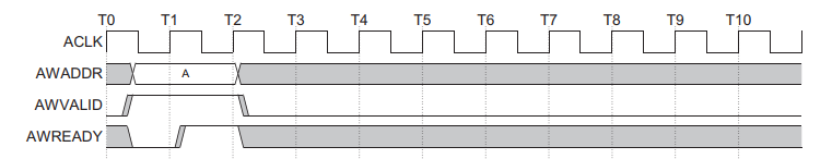
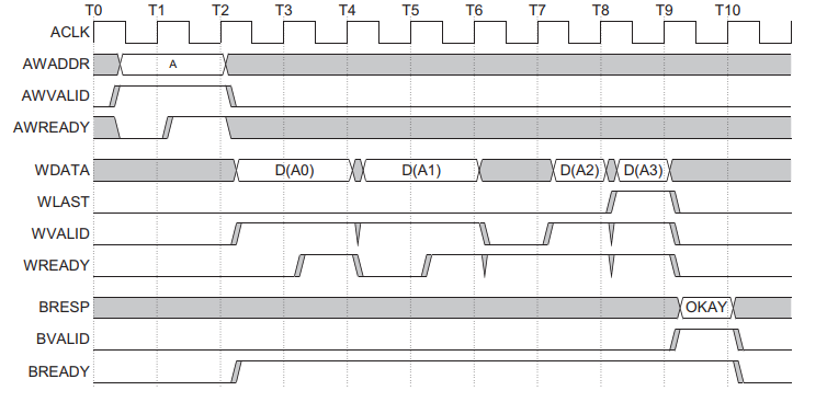
endmodule看到上面的代码还是很繁琐,不急,我给你一张图,下图为写地址通道实现,首先你需要确定你所要传输的地址,然后拉高AWVALID信号,从机那边会接收到AWVALID信号于是将AWREADY拉高,主机在编写代码时判断到AWVALID和AWREADY同时拉高时即可开始写入数据
可以看到,写地址通道的信号和逻辑并不多,但为什么输入输出端口这么多呢,因为有很多端口信号是为了拓展功能而添加的,为了减少理解难度,我尝试用AI告诉我哪些信号是固定值,哪些信号无需特别关注
可以看到ai还是解释的挺清楚的

根据波形图、官方代码注释后,就实现了写地址通道
cpp
module axi_full_master#(
    //32位基地址
    parameter  C_M_TARGET_SLAVE_BASE_ADDR	= 32'h40000000,
    //突发长度,包含1, 2, 4, 8, 16, 32, 64, 128, 256
    parameter integer C_M_AXI_BURST_LEN	= 16,
    //ID标识宽度定义
    parameter integer C_M_AXI_ID_WIDTH	= 1,
    //地址位宽
    parameter integer C_M_AXI_ADDR_WIDTH	= 32,
    //数据位宽
    parameter integer C_M_AXI_DATA_WIDTH	= 32,
    //写地址时用户自定义信号位宽
    parameter integer C_M_AXI_AWUSER_WIDTH	= 0,
    //写地址时用户自定义信号位宽
    parameter integer C_M_AXI_ARUSER_WIDTH	= 0,
    // Width of User Write Data Bus
	parameter integer C_M_AXI_WUSER_WIDTH	= 0,
	// Width of User Read Data Bus
	parameter integer C_M_AXI_RUSER_WIDTH	= 0,
	// Width of User Response Bus
	parameter integer C_M_AXI_BUSER_WIDTH	= 0
)
(
    //-------全局信号----------//
	input wire  INIT_AXI_TXN    ,//初始触发信号
	output wire  TXN_DONE       ,//发送完成
	output reg  ERROR           ,//发送错误
	input wire  M_AXI_ACLK      ,//时钟
	input wire  M_AXI_ARESETN   ,//复位
    //-------写地址信号--------//
    output wire [C_M_AXI_ID_WIDTH-1 : 0] M_AXI_AWID,//0
    output wire [C_M_AXI_ADDR_WIDTH-1 : 0] M_AXI_AWADDR,//地址
    output wire [7 : 0] M_AXI_AWLEN,//1, 2, 4, 8, 16, 32, 64, 128, 256这几个值减1,使用参数化设计上面的值,然后再减1
    output wire [2 : 0] M_AXI_AWSIZE,//用case语句网表和8/16/32/64/128/256/512/1024一一对应即可,计算方式  (数据宽度/8-1)的位宽
    output wire [1 : 0] M_AXI_AWBURST,//00地址不变,01地址递增,10地址增加到当前突发极限
    output wire  M_AXI_AWLOCK,//0
    output wire [3 : 0] M_AXI_AWCACHE,//4'b1111
    output wire [2 : 0] M_AXI_AWPROT,//0
    output wire [3 : 0] M_AXI_AWQOS,//0
    output wire [C_M_AXI_AWUSER_WIDTH-1 : 0] M_AXI_AWUSER,//0
    output wire  M_AXI_AWVALID,//实现启动信号启动时置1,接收到应答置0
    input wire  M_AXI_AWREADY,//应答
);
    wire rst_n;
    wire clk;
    assign rst_n=M_AXI_ARESETN;
    assign clk=M_AXI_ACLK;
//写地址信号
    reg [C_M_AXI_ADDR_WIDTH-1 : 0] awaddr;
    reg awvalid;
    wire burst_size_bytes;//每次突发地址增加
    assign burst_size_bytes	= C_M_AXI_BURST_LEN * C_M_AXI_DATA_WIDTH/8;
    reg bready,rready;
    reg start_reg1,start_reg2;
    always @(posedge clk) begin
        if(!rst_n)begin
            start_reg1<=0;
            start_reg2<=0;
        end
        else begin
            start_reg1<=INIT_AXI_TXN;
            start_reg2<=start_reg1;
        end
    end
    wire start_flag;
    assign start_flag=start_reg1 & !start_reg2;
/*------------------------写地址信号赋值------------------------*/
    assign M_AXI_AWID=1'b0;
    assign M_AXI_AWADDR=C_M_TARGET_SLAVE_BASE_ADDR+awaddr;//基地址加上内部逻辑设计的地址
    assign M_AXI_AWLEN=C_M_AXI_BURST_LEN-1;
    reg [2 : 0] awsize;
    assign M_AXI_AWSIZE=awsize;
    always @(*) begin
        if(!rst_n)
            awsize=0;
        else
        case (C_M_AXI_DATA_WIDTH)
             8:  awsize=3'b000;
             16: awsize=3'b001;
             32: awsize=3'b010;
             64: awsize=3'b011;
             128:awsize=3'b100;
             256:awsize=3'b101;
             512:awsize=3'b110;
             1024:awsize=3'b111;
             default: awsize=3'b010;
         endcase
    end
    assign M_AXI_AWBURST=2'b01;//突发自增,通用性比较强
    assign M_AXI_AWLOCK=1'b0;
    assign M_AXI_AWCACHE=4'b0010;//如果连接ZYNQ ACP,选择0011
    assign M_AXI_AWPROT=0;
    assign M_AXI_AWQOS=0;
    assign M_AXI_AWUSER=0;
    assign M_AXI_AWVALID=awvalid;
    reg write_start;
    reg start_w1,start_w2;
    always @(posedge clk) begin
        if(!rst_n)begin
            start_w1<=0;
            start_w2<=0;
        end
        else begin
            start_w1<=write_start;
            start_w2<=start_w1;
        end
    end
    wire startw_flag;
    assign startw_flag=start_w1 & !start_w2;
    always @(posedge clk) begin
        if(!rst_n)begin
            awvalid<=0;
        end
        else begin
            if(!awvalid&&startw_flag)//上升沿触发
                awvalid<=1;
            else if(awvalid&&M_AXI_AWREADY)
                awvalid<=0;
        end
    end
    always @(posedge clk) begin
        if(!rst_n||start_flag)begin
            awaddr<=0;
        end
        else begin
            if(awvalid&&M_AXI_AWREADY)
                awaddr<=awaddr+C_M_AXI_BURST_LEN*C_M_AXI_DATA_WIDTH/8;
            else
                awaddr<=awaddr;
        end
    end
2.写数据通道
写数据通道紧随写地址通道,波形图如下,前面那一小段还是刚刚的写地址通道,后面全是写数据通道,最下方的BRESP、BVALID和BREADY其实是写响应通道。同理在WVALID和WREADY同时拉高时数据就被写入,当写入到最后一个数据时WLAST被拉高。这里得说一下什么情况是最后一个数据,在代码的参数中定义了一个叫突发长度**//突发长度,包含1, 2, 4, 8, 16, 32, 64, 128, 256
parameter integer C_M_AXI_BURST_LEN = 16**所谓突发长度是一次写地址写数据时,我们连续写多少个数据后结束,比如下图中连续写入了四个数据,那它的突发长度就为4,当写到第四个数据时,WLAST拉高
cpp
//-------写数据信号--------//
	output wire [C_M_AXI_DATA_WIDTH-1 : 0] M_AXI_WDATA,
	output wire [C_M_AXI_DATA_WIDTH/8-1 : 0] M_AXI_WSTRB,//这一组表示突发信号的哪些字节有效,例如32位数据都有效,4'b1111
	output wire  M_AXI_WLAST,//一组突发的最后一个信号拉高
	output wire [C_M_AXI_WUSER_WIDTH-1 : 0] M_AXI_WUSER,//无需关心
	output wire  M_AXI_WVALID,
	input wire  M_AXI_WREADY,
cpp
/*------------------------写数据信号赋值------------------------*/
    reg [C_M_AXI_DATA_WIDTH-1:0] wdata;
    assign M_AXI_WDATA=wdata;
    always @(posedge clk) begin
        if(!rst_n||awvalid&&M_AXI_AWREADY)
            wdata<=1;
        else begin
            if(M_AXI_WVALID&&M_AXI_WREADY)
                wdata<=wdata+1;
            else
                wdata<=wdata;
        end
    end
    assign M_AXI_WSTRB={(C_M_AXI_DATA_WIDTH/8){1'b1}};
    assign M_AXI_WLAST=wlast;
    reg[8:0] cnt_wdata_nums;//每次突发时计数,直到完整的突发发送完毕
    always @(posedge clk) begin
        if(!rst_n||(awvalid&&M_AXI_AWREADY))
            cnt_wdata_nums<=0;
        else begin
            if(cnt_wdata_nums<C_M_AXI_BURST_LEN-1&&M_AXI_WVALID&&M_AXI_WREADY)begin
                cnt_wdata_nums<=cnt_wdata_nums+1;
            end
        end
    end
    assign TXN_DONE=((cnt_wdata_nums==C_M_AXI_BURST_LEN-1)&&M_AXI_WVALID&&M_AXI_WREADY)?1:0;
    assign M_AXI_WUSER=0;
    reg wvalid;
    assign M_AXI_WVALID=wvalid;
    always @(posedge clk) begin
        if(!rst_n)
            wvalid<=0;
        else begin
            if(awvalid&&M_AXI_AWREADY)
                wvalid<=1;
            else if(wlast)
                wvalid<=0;
        end
    end
3.写响应通道
还是这幅图,最下方B开头的三个信号就是响应信号,响应信号为我们提供了数据传输是否出错,当BVALID和VREADY同时被拉高时我们读取BRESP,为2'b00为成功写入
代码如下:
cpp
//-------写响应信号--------//
	input wire [C_M_AXI_ID_WIDTH-1 : 0] M_AXI_BID,
	input wire [1 : 0] M_AXI_BRESP,//00应答成功、01独占访问成功、10从机错误(如地址无效)、解码错误(如无从机)
	//input wire [C_M_AXI_BUSER_WIDTH-1 : 0] M_AXI_BUSER,//用户自定义信号,无需关心
	input wire  M_AXI_BVALID,
	output wire  M_AXI_BREADY,
cpp
assign M_AXI_BREADY=bready;
    always @(posedge clk) begin
        if(!rst_n)
            bready<=0;
        else begin
            if(awvalid&&M_AXI_AWREADY)
                bready<=1;
            else if(bready&&M_AXI_BVALID)
                bready<=0;
        end
    end
    reg [1 : 0] bresp;
    always @(posedge clk) begin
        if(!rst_n||awvalid&&M_AXI_AWREADY)
            bresp<=0;
        else
            if(bready&&M_AXI_BVALID)
                bresp<=M_AXI_BRESP;
    end
4.读地址通道和读数据通道
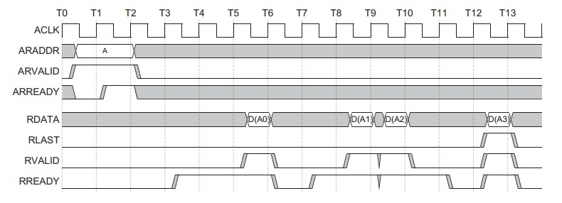
波形图如下:
代码如下:
cpp
//-------读地址信号--------//
	output wire [C_M_AXI_ID_WIDTH-1 : 0] M_AXI_ARID,//读数据地址ID,0
	output wire [C_M_AXI_ADDR_WIDTH-1 : 0] M_AXI_ARADDR,//读数据地址
	output wire [7 : 0] M_AXI_ARLEN,//读数据突发长度,1, 2, 4, 8, 16, 32, 64, 128, 256这几个值减1,使用参数化设计上面的值,然后再减1
	output wire [2 : 0] M_AXI_ARSIZE,//读数据宽度,用case语句网表和8/16/32/64/128/256/512/1024一一对应即可
	output wire [1 : 0] M_AXI_ARBURST,//突发类型,01
	output wire  M_AXI_ARLOCK,//0
	output wire [3 : 0] M_AXI_ARCACHE,//4'b1111
	output wire [2 : 0] M_AXI_ARPROT,//0
	output wire [3 : 0] M_AXI_ARQOS,//0
	output wire [C_M_AXI_ARUSER_WIDTH-1 : 0] M_AXI_ARUSER,//0
	output wire  M_AXI_ARVALID,
	input wire  M_AXI_ARREADY,
//-------读数据信号--------//
	input wire [C_M_AXI_ID_WIDTH-1 : 0] M_AXI_RID,//0
	input wire [C_M_AXI_DATA_WIDTH-1 : 0] M_AXI_RDATA,//数据
	input wire [1 : 0] M_AXI_RRESP,//反映是否出错
	input wire  M_AXI_RLAST,
	input wire [C_M_AXI_RUSER_WIDTH-1 : 0] M_AXI_RUSER,//0,自定义信号,无特别需求
	input wire  M_AXI_RVALID,
	output wire  M_AXI_RREADY
cpp
/*------------------------读地址信号赋值------------------------*/
    assign M_AXI_ARID=1'b0;
    reg [C_M_AXI_ADDR_WIDTH-1 : 0] araddr;
    wire rlast;
    assign rlast=M_AXI_RLAST;
    assign M_AXI_ARADDR=C_M_TARGET_SLAVE_BASE_ADDR+araddr;
    always @(posedge clk) begin
        if(!rst_n||start_flag)
            araddr<=0;
        else begin
            if(rlast&&M_AXI_RREADY&&M_AXI_RVALID)
                araddr<=araddr+C_M_AXI_BURST_LEN*C_M_AXI_DATA_WIDTH/8;
        end
    end
    assign M_AXI_ARLEN=C_M_AXI_BURST_LEN-1;
    reg [2 : 0] arsize;
    assign M_AXI_ARSIZE=arsize;
    always @(*) begin
        if(!rst_n)
            arsize=0;
        else
        case (C_M_AXI_DATA_WIDTH)
             8:  arsize=3'b000;
             16: arsize=3'b001;
             32: arsize=3'b010;
             64: arsize=3'b011;
             128:arsize=3'b100;
             256:arsize=3'b101;
             512:arsize=3'b110;
             1024:arsize=3'b111;
             default: arsize=3'b010;
         endcase
    end
    assign M_AXI_ARBURST=2'b01;
    assign M_AXI_ARLOCK=0;
    assign M_AXI_ARCACHE=4'b1111;
    assign M_AXI_ARPROT=0;
    assign M_AXI_ARQOS=0;
    assign M_AXI_ARUSER=0;
    reg read_start;//一次完整读突发启动
    reg start_r1,start_r2;
    always @(posedge clk) begin
        if(!rst_n)begin
            start_r1<=0;
            start_r2<=0;
        end
        else begin
            start_r1<=read_start;
            start_r2<=start_r1;
        end
    end
    wire startr_flag;
    assign startr_flag=start_r1 & !start_r2;
    reg arvalid;
    always @(posedge clk) begin
        if(!rst_n)
            arvalid<=0;
        else begin
            if(!arvalid&&startr_flag)
                arvalid<=1;
            else if(arvalid&&M_AXI_ARREADY)
                arvalid<=0;
        end
    end
    assign M_AXI_ARVALID=arvalid;
/*------------------------读数据信号赋值------------------------*/
    reg [C_M_AXI_DATA_WIDTH-1 : 0] rdata_reg;
    reg rvalid;
    assign M_AXI_RREADY=rready;
    always @(posedge clk) begin
        if(!rst_n)
            rready<=0;
        else begin
            if(arvalid&&M_AXI_ARREADY)
                rready<=1;
            else if(M_AXI_RLAST&&M_AXI_RVALID&&M_AXI_RREADY)
                rready<=0;
        end
    end
补充代码,上面这些通道编写时漏掉的:
cpp
 wire wlast;
    assign wlast=(cnt_wdata_nums==C_M_AXI_BURST_LEN-1&&M_AXI_WVALID&&M_AXI_WREADY)?1:0;
    assign write_resp_error = bready & M_AXI_BVALID & M_AXI_BRESP[1];
    assign read_resp_error = rready & M_AXI_RVALID & M_AXI_RRESP[1];
    always @(posedge clk) begin
        if(!rst_n||start_flag)
            ERROR<=0;
        else
            if(write_resp_error||read_resp_error)
                ERROR<=1;
            else
                ERROR<=ERROR;
    end
5.状态机设计
cpp
/*------------------------状态机设计------------------------*/
//目的,先写一组突发,再读一组突发

reg [2:0] cur_state,next_state;
parameter IDLE = 3'b000,
          WDATA= 3'b001,
          RDATA= 3'b010;

    always @(posedge clk) begin
        if(!rst_n)
            cur_state<=IDLE;
        else
            cur_state<=next_state;
    end
    always @(*) begin
        if(!rst_n)
            next_state<=IDLE;
        else begin
            case (cur_state)
            IDLE :begin
                if(start_flag)
                    next_state<=WDATA;
                else
                    next_state<=IDLE;
            end
            WDATA:begin
                if(wlast)
                    next_state<=RDATA;
                else
                    next_state<=WDATA;
            end
            RDATA:begin
                if(rlast&&M_AXI_RVALID&&M_AXI_RREADY)
                    next_state<=IDLE;
                else
                    next_state<=RDATA;
            end
                default: next_state<=IDLE;
            endcase
        end
    end
    always @(posedge clk) begin
        if(!rst_n)begin
            write_start<=0;
            read_start<=0;
        end
        else begin
            case (cur_state)
            IDLE :begin
                write_start<=0;
                read_start<=0;
            end
            WDATA:begin
                if(wlast)
                    write_start<=0;
                else
                    write_start<=1;
                read_start<=0;
            end
            RDATA:begin
                write_start<=0;
                read_start<=1;
            end
                default: ;
            endcase
        end
    end
代码验证
testbench代码
cpp
`timescale 1ns/1ns

module axi_tb();

// -------------------------- 时钟和复位信号 --------------------------
reg M_AXI_ACLK;       // 主时钟
reg M_AXI_ARESETN;    // 复位信号(低有效)

// -------------------------- 主设备控制信号 --------------------------
reg INIT_AXI_TXN;     // 启动事务信号
wire TXN_DONE;        // 事务完成信号
wire ERROR;           // 错误信号

// -------------------------- AXI主从接口信号(连接主设备和从设备) --------------------------
// 写地址通道
wire [0:0] M_AXI_AWID;
wire [31:0] M_AXI_AWADDR;
wire [7:0] M_AXI_AWLEN;
wire [2:0] M_AXI_AWSIZE;
wire [1:0] M_AXI_AWBURST;
wire M_AXI_AWLOCK;
wire [3:0] M_AXI_AWCACHE;
wire [2:0] M_AXI_AWPROT;
wire [3:0] M_AXI_AWQOS;
wire M_AXI_AWUSER;
wire M_AXI_AWVALID;
reg M_AXI_AWREADY;    // 从设备应答:及时响应写地址

// 写数据通道
wire [31:0] M_AXI_WDATA;
wire [3:0] M_AXI_WSTRB;
wire M_AXI_WLAST;
wire M_AXI_WUSER;
wire M_AXI_WVALID;
reg M_AXI_WREADY;     // 从设备应答:及时响应写数据

// 写响应通道
wire [0:0] M_AXI_BID;
reg [1:0] M_AXI_BRESP;  // 写响应:00表示成功
wire M_AXI_BUSER;
reg M_AXI_BVALID;       // 写响应有效
wire M_AXI_BREADY;

// 读地址通道
wire [0:0] M_AXI_ARID;
wire [31:0] M_AXI_ARADDR;
wire [7:0] M_AXI_ARLEN;
wire [2:0] M_AXI_ARSIZE;
wire [1:0] M_AXI_ARBURST;
wire M_AXI_ARLOCK;
wire [3:0] M_AXI_ARCACHE;
wire [2:0] M_AXI_ARPROT;
wire [3:0] M_AXI_ARQOS;
wire M_AXI_ARUSER;
wire M_AXI_ARVALID;
reg M_AXI_ARREADY;    // 从设备应答:及时响应读地址

// 读数据通道
wire [0:0] M_AXI_RID;
reg [31:0] M_AXI_RDATA;  // 读数据:返回主设备写入的值
reg [1:0] M_AXI_RRESP;   // 读响应:00表示成功
reg M_AXI_RLAST;         // 读最后一个数据标记
wire M_AXI_RUSER;
reg M_AXI_RVALID;        // 读数据有效
wire M_AXI_RREADY;

// -------------------------- 时钟生成(100MHz) --------------------------
initial begin
    M_AXI_ACLK = 1'b0;
    forever #5 M_AXI_ACLK = ~M_AXI_ACLK;  // 周期10ns
end

// -------------------------- 复位和启动信号生成 --------------------------
initial begin
    // 初始状态:复位有效,启动信号无效
    M_AXI_ARESETN = 1'b0;
    INIT_AXI_TXN = 1'b0;

    #100;  // 复位100ns
    M_AXI_ARESETN = 1'b1;  // 释放复位

    #50;   // 等待50ns
    INIT_AXI_TXN = 1'b1;   // 拉高启动信号
    #30;    // 保持3个时钟周期
    INIT_AXI_TXN = 1'b0;   // 拉低启动信号

    // 仿真运行足够长时间(确保完成一次读写)
    #10000;  // 10000ns后自动结束
end

// -------------------------- 实例化待测试的AXI主设备 --------------------------
axi_full_master #(
    .C_M_TARGET_SLAVE_BASE_ADDR(32'h40000000),  // 从设备基地址
    .C_M_AXI_BURST_LEN(4),                      // 突发长度4(简化波形观测)
    .C_M_AXI_ID_WIDTH(1),
    .C_M_AXI_ADDR_WIDTH(32),
    .C_M_AXI_DATA_WIDTH(32)                     // 32位数据
) u_axi_full_master (
    .INIT_AXI_TXN(INIT_AXI_TXN),
    .TXN_DONE(TXN_DONE),
    .ERROR(ERROR),
    .M_AXI_ACLK(M_AXI_ACLK),
    .M_AXI_ARESETN(M_AXI_ARESETN),
    // 写地址通道
    .M_AXI_AWID(M_AXI_AWID),
    .M_AXI_AWADDR(M_AXI_AWADDR),
    .M_AXI_AWLEN(M_AXI_AWLEN),
    .M_AXI_AWSIZE(M_AXI_AWSIZE),
    .M_AXI_AWBURST(M_AXI_AWBURST),
    .M_AXI_AWLOCK(M_AXI_AWLOCK),
    .M_AXI_AWCACHE(M_AXI_AWCACHE),
    .M_AXI_AWPROT(M_AXI_AWPROT),
    .M_AXI_AWQOS(M_AXI_AWQOS),
    .M_AXI_AWUSER(M_AXI_AWUSER),
    .M_AXI_AWVALID(M_AXI_AWVALID),
    .M_AXI_AWREADY(M_AXI_AWREADY),
    // 写数据通道
    .M_AXI_WDATA(M_AXI_WDATA),
    .M_AXI_WSTRB(M_AXI_WSTRB),
    .M_AXI_WLAST(M_AXI_WLAST),
    .M_AXI_WUSER(M_AXI_WUSER),
    .M_AXI_WVALID(M_AXI_WVALID),
    .M_AXI_WREADY(M_AXI_WREADY),
    // 写响应通道
    .M_AXI_BID(M_AXI_BID),
    .M_AXI_BRESP(M_AXI_BRESP),
    .M_AXI_BVALID(M_AXI_BVALID),
    .M_AXI_BREADY(M_AXI_BREADY),
    // 读地址通道
    .M_AXI_ARID(M_AXI_ARID),
    .M_AXI_ARADDR(M_AXI_ARADDR),
    .M_AXI_ARLEN(M_AXI_ARLEN),
    .M_AXI_ARSIZE(M_AXI_ARSIZE),
    .M_AXI_ARBURST(M_AXI_ARBURST),
    .M_AXI_ARLOCK(M_AXI_ARLOCK),
    .M_AXI_ARCACHE(M_AXI_ARCACHE),
    .M_AXI_ARPROT(M_AXI_ARPROT),
    .M_AXI_ARQOS(M_AXI_ARQOS),
    .M_AXI_ARUSER(M_AXI_ARUSER),
    .M_AXI_ARVALID(M_AXI_ARVALID),
    .M_AXI_ARREADY(M_AXI_ARREADY),
    // 读数据通道
    .M_AXI_RID(M_AXI_RID),
    .M_AXI_RDATA(M_AXI_RDATA),
    .M_AXI_RRESP(M_AXI_RRESP),
    .M_AXI_RLAST(M_AXI_RLAST),
    .M_AXI_RUSER(M_AXI_RUSER),
    .M_AXI_RVALID(M_AXI_RVALID),
    .M_AXI_RREADY(M_AXI_RREADY)
);

// -------------------------- 简易从设备:及时应答+存储数据(供波形观测) --------------------------
reg [31:0] slave_mem [0:3];  // 存储4个突发数据(配合BURST_LEN=4)
reg [1:0] w_cnt, r_cnt;      // 突发计数器(0~3)

// 1. 写地址通道:主设备发VALID后,从设备立即应答READY
always @(posedge M_AXI_ACLK or negedge M_AXI_ARESETN) begin
    if (!M_AXI_ARESETN) begin
        M_AXI_AWREADY <= 1'b0;
    end else begin
        M_AXI_AWREADY <= M_AXI_AWVALID;  // 及时应答
    end
end

// 2. 写数据通道:主设备发VALID后,从设备立即应答READY,并存储数据
always @(posedge M_AXI_ACLK or negedge M_AXI_ARESETN) begin
    if (!M_AXI_ARESETN) begin
        M_AXI_WREADY <= 1'b0;
        w_cnt <= 2'd0;
    end else begin
        M_AXI_WREADY <= M_AXI_WVALID;  // 及时应答
        if (M_AXI_WVALID && M_AXI_WREADY) begin
            slave_mem[w_cnt] <= M_AXI_WDATA;  // 存储数据
            w_cnt <= w_cnt + 1'b1;            // 计数
        end
    end
end

// 3. 写响应通道:写完成后返回成功响应
always @(posedge M_AXI_ACLK or negedge M_AXI_ARESETN) begin
    if (!M_AXI_ARESETN) begin
        M_AXI_BVALID <= 1'b0;
        M_AXI_BRESP <= 2'b00;  // 00=成功
    end else begin
        if (M_AXI_WLAST && M_AXI_WVALID && M_AXI_WREADY) begin
            M_AXI_BVALID <= 1'b1;  // 最后一个数据写完,发响应
        end else if (M_AXI_BREADY) begin
            M_AXI_BVALID <= 1'b0;  // 响应被接收后拉低
        end
    end
end

// 4. 读地址通道:主设备发VALID后,从设备立即应答READY
always @(posedge M_AXI_ACLK or negedge M_AXI_ARESETN) begin
    if (!M_AXI_ARESETN) begin
        M_AXI_ARREADY <= 1'b0;
    end else begin
        M_AXI_ARREADY <= M_AXI_ARVALID;  // 及时应答
    end
end

// 新增:写数据时按顺序存储
always @(posedge M_AXI_ACLK or negedge M_AXI_ARESETN) begin
    if (!M_AXI_ARESETN) begin
        w_cnt <= 2'd0;
    end else if (M_AXI_WVALID && M_AXI_WREADY) begin
        slave_mem[w_cnt] <= M_AXI_WDATA;  // 按顺序存储写数据
        w_cnt <= (M_AXI_WLAST) ? 2'd0 : w_cnt + 1'b1;  // 最后一个数据后复位计数
    end
end

// 5. 读数据通道:修复数据顺序和RLAST拉低问题
always @(posedge M_AXI_ACLK or negedge M_AXI_ARESETN) begin
    if (!M_AXI_ARESETN) begin
        M_AXI_RVALID <= 1'b0;
        M_AXI_RDATA <= 32'h0;
        M_AXI_RLAST <= 1'b0;  // 复位时拉低
        M_AXI_RRESP <= 2'b00;
        r_cnt <= 2'd0;
    end else begin
        // 读地址握手后,启动读数据传输
        if (M_AXI_ARVALID && M_AXI_ARREADY) begin  // 用握手信号判断读启动(更准确)
            M_AXI_RVALID <= 1'b1;
            M_AXI_RDATA <= slave_mem[0];  // 从第一个存储数据开始读
            r_cnt <= 2'd1;  // 下一个数据索引为1
        end
        // 主设备准备好接收,且从设备数据有效时
        else if (M_AXI_RREADY && M_AXI_RVALID) begin
            if (r_cnt == 2'd3) begin  // 第4个数据(索引3)是最后一个
                M_AXI_RDATA <= slave_mem[3];
                M_AXI_RLAST <= 1'b1;  // 拉高LAST
                M_AXI_RVALID <= 1'b1; // 传输完成,拉低VALID
                r_cnt <= 2'd4;        // 复位计数
            end else if (r_cnt < 2'd3) begin  // 中间数据(1、2)
                M_AXI_RDATA <= slave_mem[r_cnt];
                r_cnt <= r_cnt + 1'b1;
                M_AXI_RLAST <= 1'b0;  // 保持LAST为低
            end else begin  // 最后一个数据传输完成后,强制拉低LAST
                M_AXI_RLAST <= 1'b0;
            end
        end
    end
end

endmodule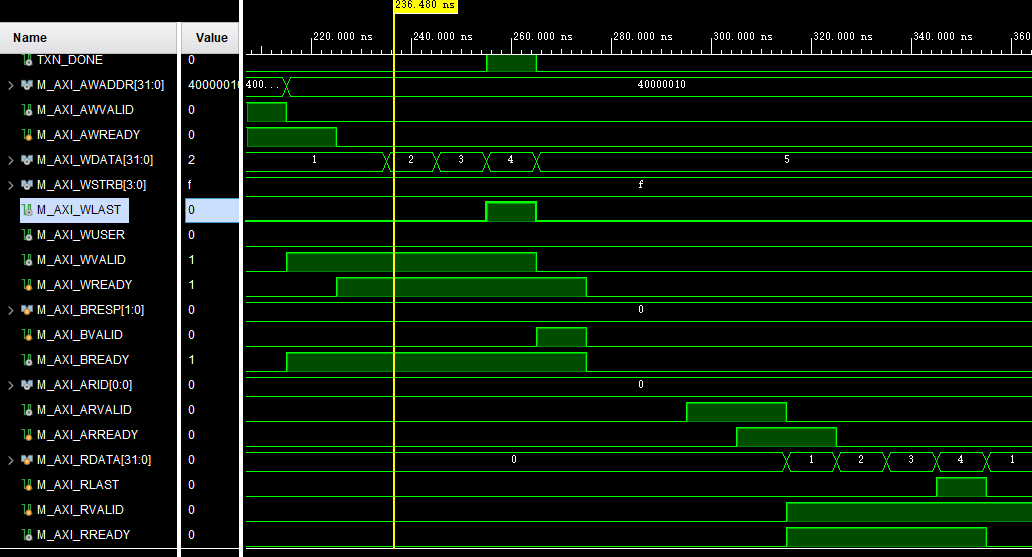
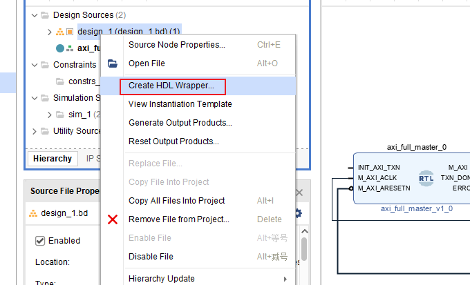
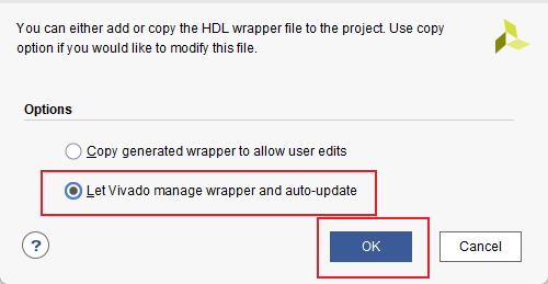
上板验证
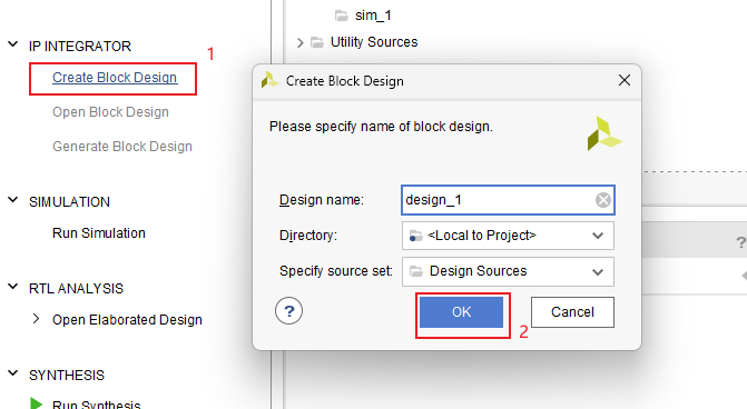
创建一个新项目后左侧点击Create Block Design,然后点OK
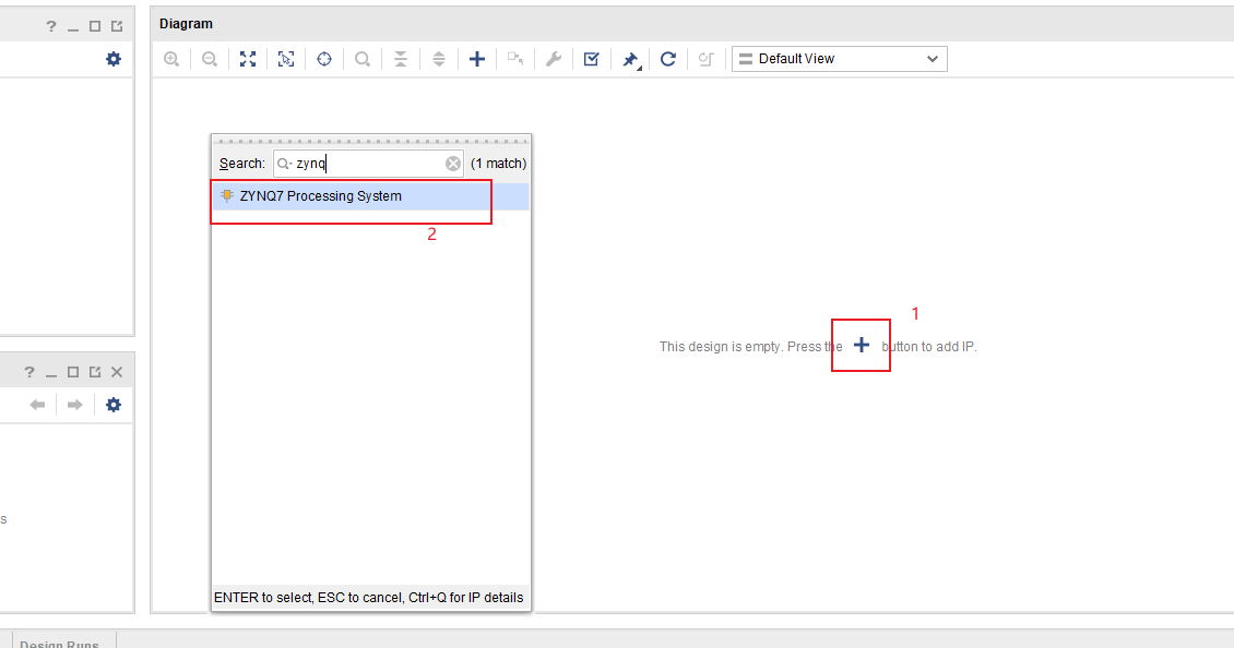
添加zynq模块
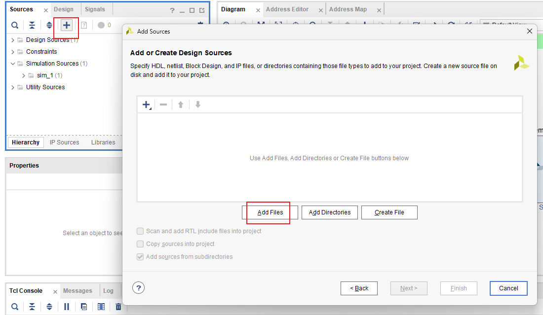
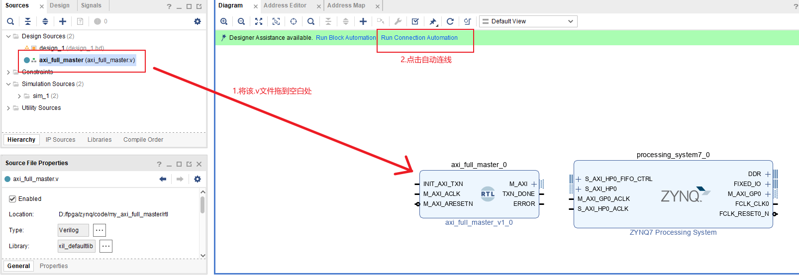
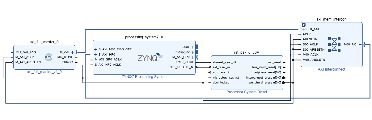
添加写好的AXI代码
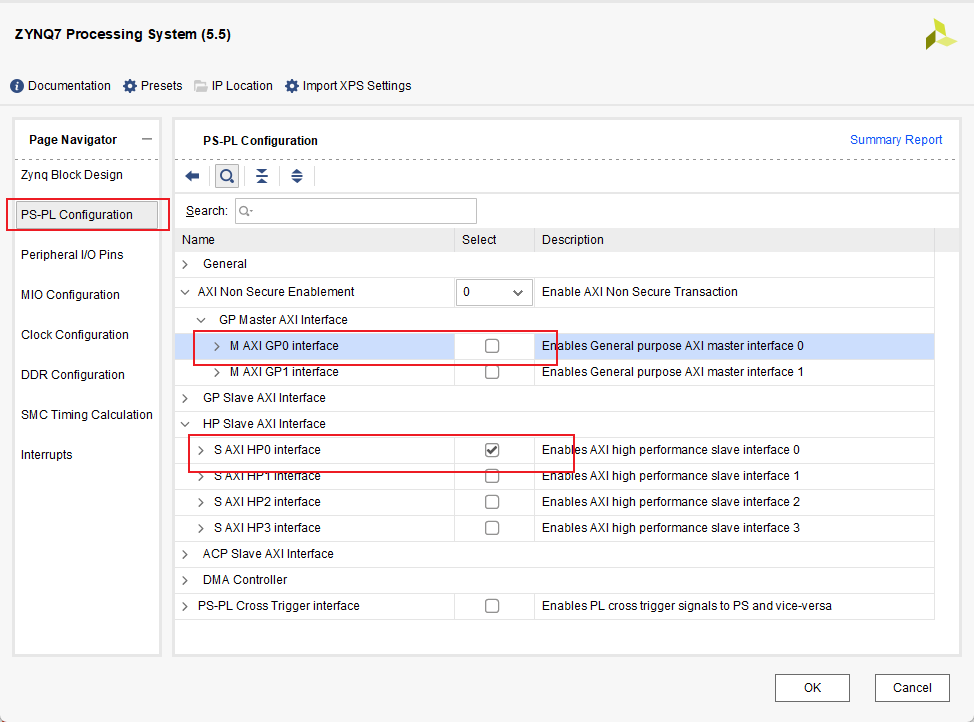
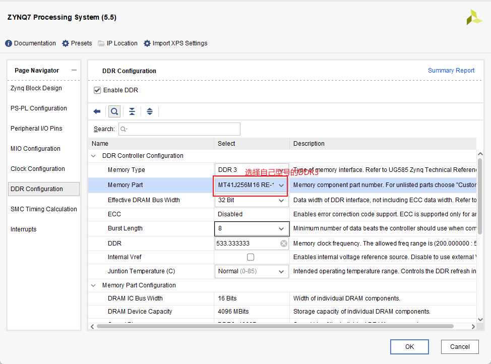
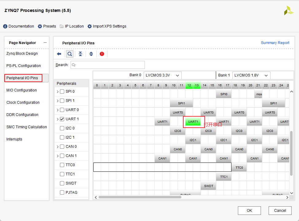
配置zynq,打开AXI HP,它是zynq上连接ddr3的模块,其连线逻辑为AXI FULL从机
点击ok
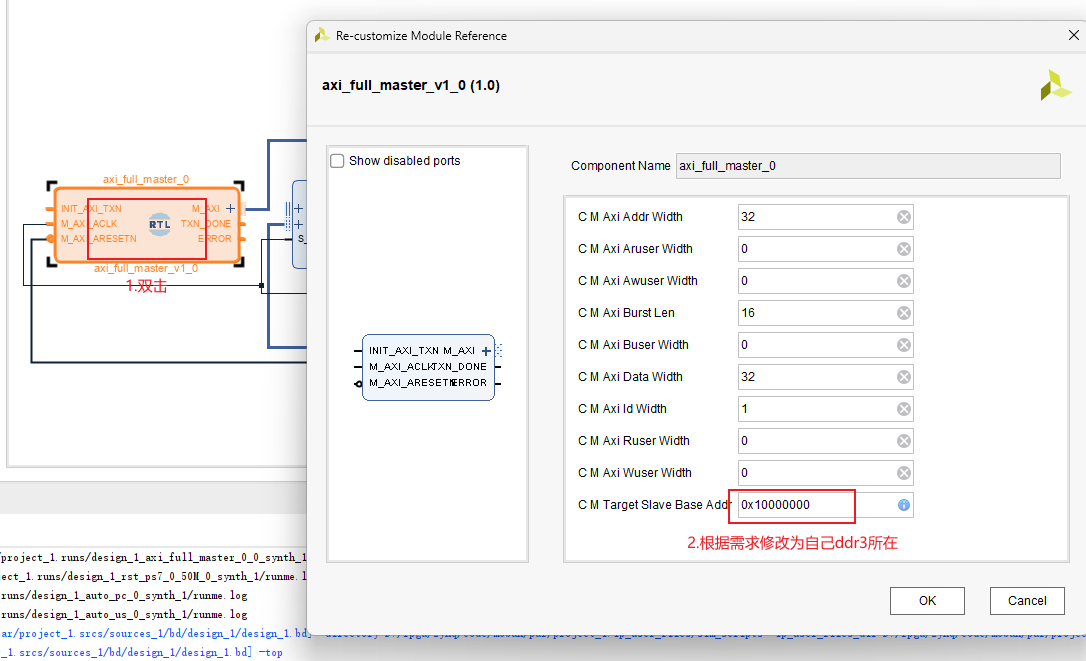
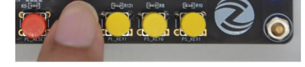
再创建一个按键消抖模块作为启动信号,创建好代码后拖到空白处,然后连接INIT_AXI_TXN
代码:
cpp
`timescale 1ns / 1ps

module key_filliter#(parameter delay = 49_9)(
        input clk,
        input rst_n,
        input key,
        output key_flag
    );
    reg[11:0] cnt;
    always@(posedge clk)begin
        if(!rst_n)
            cnt<=0;
        else begin
            if(key==0)begin
                if(cnt==delay)
                    cnt<=cnt;//cnt保持
                else
                    cnt<=cnt+1;
            end
            else
                cnt<=0;
        end
    end

    //key_flag取决于cnt
    assign key_flag=(cnt==delay-1)? 1: 0;
endmodule
拖入后按如下操作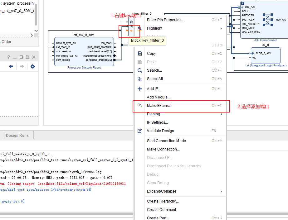
将按键消抖模块连线,完成后如下,可根据需求添加ila,没有也没事
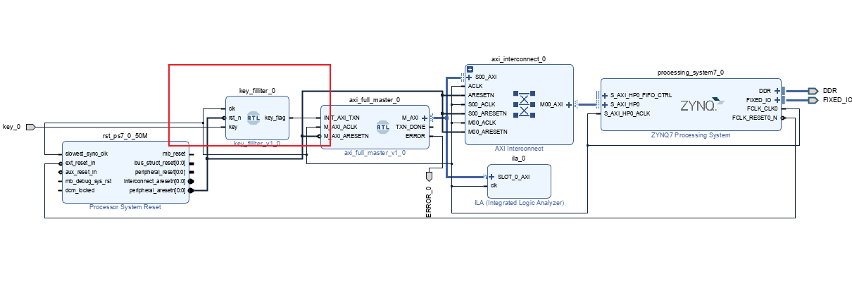
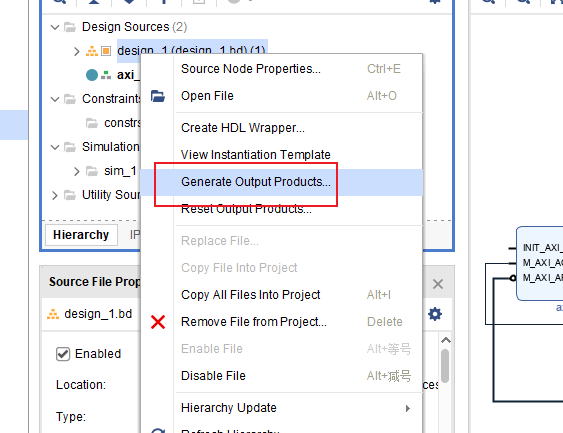
生成顶层文件
创建约束文件
cpp
set_property IOSTANDARD LVCMOS33 [get_ports key_0]
set_property PACKAGE_PIN L14 [get_ports key_0]

set_property IOSTANDARD LVCMOS33 [get_ports ERROR_0]
set_property PACKAGE_PIN L15 [get_ports ERROR_0]
生成bit流
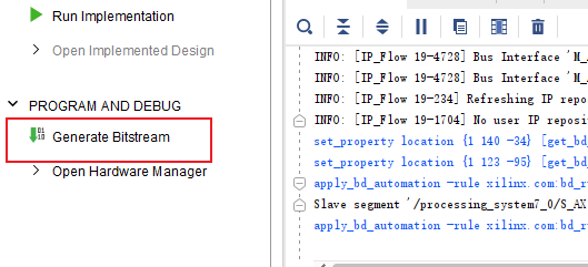
生成后准备烧写到zynq上
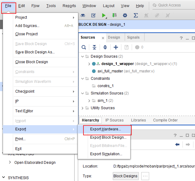
选择包含bit流文件
选择文件地址后我们打开VITIS,按步骤把上图建立的文件导入,建立好zynq空项目
创建c语言文件,代码如下
cpp
#include <stdio.h>
#include "xil_cache.h"
#include "xil_printf.h"
#include "xil_io.h"
int main()
{
int i;
char c;
Xil_DCacheDisable(); // 关闭数据缓存,确保直接访问物理地址
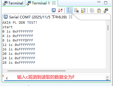
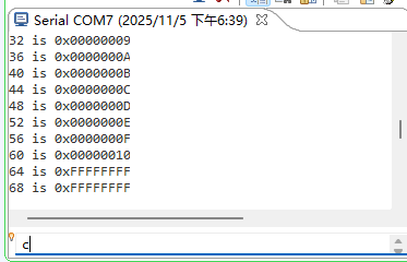
xil_printf("AXI4 PL DDR TEST!\n\r"); // 使用xilinx推荐的打印函数
while(1)
{
scanf("%c", &c); // 等待输入字符
if(c == 'c') // 输入'c'时触发读取操作
{
xil_printf("start\n\r");
// 读取0x10000000开始的400字节
//在fpga端代码是发送一次完整突发写,突发长度为16,每次突发传输的数据+1,位宽是32位
//实验现象预测,每一个地址对应8位数据,一次完整突发要发送16个32位数据,所以每次读的地址+4个字节也就是32位
//第一次突发写,写入32位数据1、第二次突发写写入32位数据2...一直持续到第16次突发写,完整的突发写入结束
for(i = 0; i < 400; i += 4)
{
xil_printf("%d is 0x%08x\n\r", i, Xil_In32(0x10000000 + i));
}
}
}
return 0;
}编译后选择烧录包含FPGA
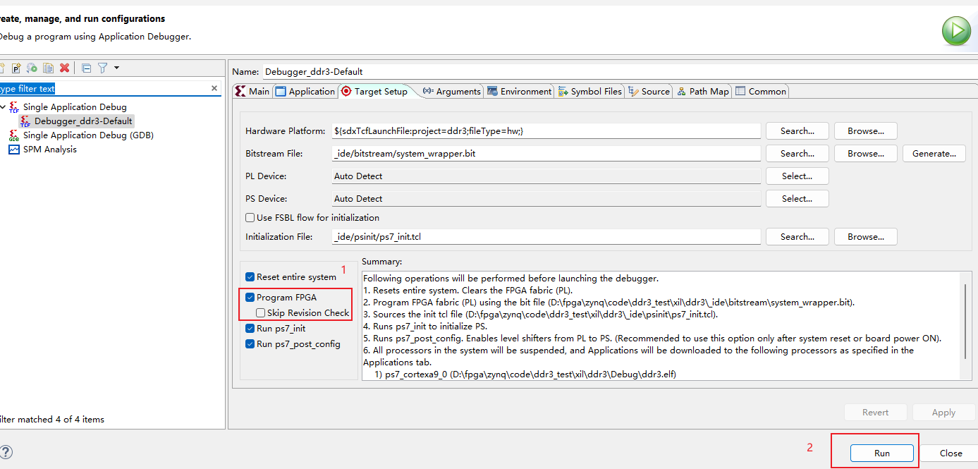
烧录完成
按下按钮
再次向串口输出c,可以看到地址被写入数据,写了16个32位数据
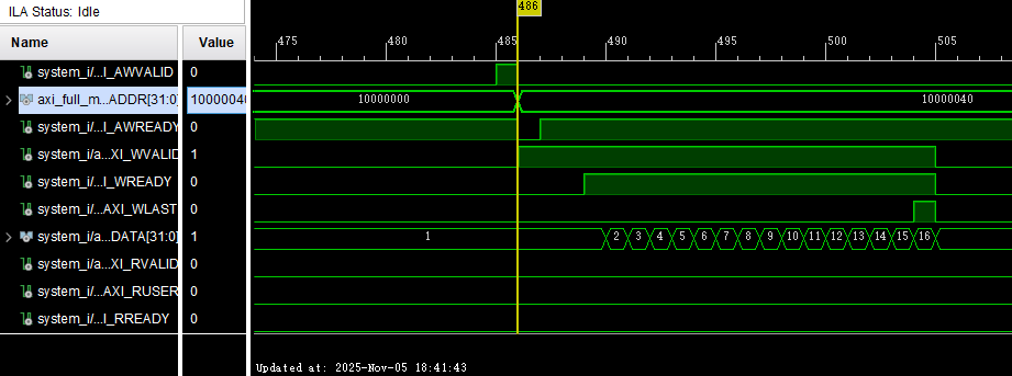
ILA示波器验证
写数据
读数据
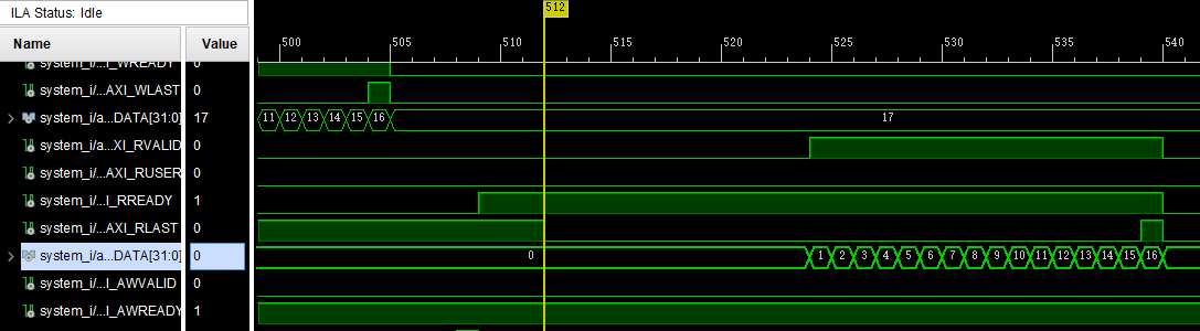
可以看到这里RLAST在默认情况下竟然是被拉高的情况,这里我调试了好久发现了这个问题,最终将AXI代码中的读通道不仅仅依靠RLAST变化才让功能正确,其问题出现在自动连线时生成的axi interconnect的ip核逻辑