1、之前分享的简易操作说明'
H7-TOOL的LUA小程序访问AP和DP调试寄存器方法(2023-08-16)
https://forum.anfulai.cn/forum.php?mod=viewthread&tid=120658
2 、AP和DP寄存器是通过调试接口访问芯片各种内存,寄存器和外设的基础。
格式
Lua
------------------------------------------------------------------------------------------
--                         SWD Packet format                                             |
------------------------------------------------------------------------------------------
--| Start | APnDP | RnW | Addr[2:3] | Parity | STOP | Park | ACK response | Data | Parity|
-----------------------------------------------------------------------------------------
--|  1bit | 1bit  | 1bit| 2bits     | 1bit   | 1bit | 1bit | 3bits        | 32bits| 1bit |
------------------------------------------------------------------------------------------
-- Start       : 1 bit, always 1
-- APnDP       : 1 bit, 0 for DP access, 1 for AP access
-- RnW         : 1 bit, 0 for write, 1 for read
-- Addr[2:3]   : 2 bits, the address of the register to access,
--               must be aligned to 4 bytes, so the lower 2 bits are always 0
-- Parity      : 1 bit, the parity of APnDP, RnW and Addr[2:3], must be even parity
-- STOP        : 1 bit, always 0
-- Park        : 1 bit, always 1
-- ACK response: 3 bits, can be OK (001), WAIT (010), FAULT (100) or Protocol Error (000)
-- Data        : 32 bits for read or write data,WDATAP[31:0], RDATAP[31:0] and Parity
Lua
----------------------------------------------------------------------------
----------------------------------------------------------------------------
--DP AP寄存器定义
function SWD_RegDefine(void)
--DP Addr, Debug Port Register Addresses,
DP0_IDCODE = 0x00 --R, IDCODE Register (SW Read only)
DP0_ABORT = 0x00 --W, Abort Register (SW Write only)
DP4_CTRL_STAT= 0x04 --RW, DPBANKSEL = 0, Control & Status,It controls the DP and provides status information
DP4_DLCR = 0x04 --RW, DPBANKSEL = 1, It controls the operating mode of the SWD Data Link(SW Only)
DP4_TARGETID = 0x04 --RW, DPBANKSEL = 2, It provides target identification information
DP4_DLPIDR = 0x04 --RW, DPBANKSEL = 3, It provides the SWD protocol version(SW Only)
DP4_RESERVED = 0x04 --RW, DPBANKSEL = 0x04 - 0x0F are reserved for future use
DP8_RESEND = 0x08 --R, It returns the value that was returned by the last AP
--read or DP_RDBUFF read, used in the event of a corrupted read transfer. (SW Read Only)
DP8_SELECT = 0x08 --W, Select DP4 Register (JTAG R/W & SW W)
DPc_RDBUFF = 0x0C --R, Read Buffer
DPc_TARGETSEL= 0x0C --W, Select target following a line reset sequence, (JTAG R/W & SW W)
-- Bits [31:28] match bits DP_DLPIDR[31:28]
-- Bits [27:0] match bits DP_TARGETID[27:0]
--Debug Select Register definitions
-- #define CTRLSEL 0x00000001 // CTRLSEL (SW Only)
-- #define APBANKSEL 0x000000F0 // APBANKSEL Mask
-- #define APSEL 0xFF000000 // APSEL Mask
--AP Addr, Access Port Register Addresses
AP0_CSW = 0x00 --Control and Status Word
AP4_TAR = 0x04 --Transfer Address
AP8 = 0X08
APc_DRW = 0x0C --Data Read/Write
AP10_BD0 = 0x10 --Banked Data 0
AP14_BD1 = 0x14 --Banked Data 1
AP18_BD2 = 0x18 --Banked Data 2
AP1c_BD3 = 0x1C --Banked Data 3
APf8_ROM = 0xF8 --Debug ROM Address
APfc_IDR = 0xFC --Identification Register
-- DP0_ABORT, Abort Register definitions
DAPABORT = 0x00000001 -- DAP Abort transac1tion
STKCMPCLR = 0x00000002 -- Clear CTRL/STAT STICKYCMP Flag (SW Only)
STKERRCLR = 0x00000004 -- Clear CTRL/STAT STICKYERR Flag (SW Only)
WDERRCLR = 0x00000008 -- Clear CTRL/STAT WDATAERR Flag (SW Only)
ORUNERRCLR = 0x00000010 -- Clear CTRL/STAT STICKYORUN Flag (SW Only)
-- DP4_CTRL_STAT, Debug Control and Status definitions
ORUNDETECT = 0x00000001 -- Overrun Detect
STICKYORUN = 0x00000002 -- Sticky Overrun
TRNMODE = 0x0000000C -- Transfer Mode Mask
TRNNORMAL = 0x00000000 -- Transfer Mode: Normal
TRNVERIFY = 0x00000004 -- Transfer Mode: Pushed Verify
TRNCOMPARE = 0x00000008 -- Transfer Mode: Pushed Compare
STICKYCMP = 0x00000010 -- Sticky Compare
STICKYERR = 0x00000020 -- Sticky Error
READOK = 0x00000040 -- Read OK (SW Only)
WDATAERR = 0x00000080 -- Write Data Error (SW Only)
MASKLANE = 0x00000F00 -- Mask Lane Mask
MASKLANE0 = 0x00000100 -- Mask Lane 0
MASKLANE1 = 0x00000200 -- Mask Lane 1
MASKLANE2 = 0x00000400 -- Mask Lane 2
MASKLANE3 = 0x00000800 -- Mask Lane 3
TRNCNT = 0x001FF000 -- Transaction Counter Mask
CDBGRSTREQ = 0x04000000 -- Debug Reset Request
CDBGRSTACK = 0x08000000 -- Debug Reset Acknowledge
CDBGPWRUPREQ = 0x10000000 -- Debug Power-up Request
CDBGPWRUPACK = 0x20000000 -- Debug Power-up Acknowledge
CSYSPWRUPREQ = 0x40000000 -- System Power-up Request
CSYSPWRUPACK = 0x80000000 -- System Power-up Acknowledge
-- AP0_CSW, AP Control and Status Word definitions
CSW_SIZE =0x00000007 -- Access Size: Selection Mask
CSW_SIZE8 =0x00000000 -- Access Size: 8-bit
CSW_SIZE16 =0x00000001 -- Access Size: 16-bit
CSW_SIZE32 =0x00000002 -- Access Size: 32-bit
CSW_ADDRINC =0x00000030 -- Auto Address Increment Mask
CSW_NADDRINC =0x00000000 -- No Address Increment
CSW_SADDRINC =0x00000010 -- Single Address Increment
CSW_PADDRINC =0x00000020 -- Packed Address Increment
CSW_DBGSTAT =0x00000040 -- Debug Status
CSW_TINPROG =0x00000080 -- Transfer in progress
CSW_HPROT =0x02000000 -- User/Privilege Control
CSW_MSTRTYPE =0x20000000 -- Master Type Mask
CSW_MSTRCORE =0x00000000 -- Master Type: Core
CSW_MSTRDBG =0x20000000 -- Master Type: Debug
CSW_RESERVED =0x01000000 -- Reserved Value
--Core Debug Register Addresses
DBG_HCSR = 0xe000edf0
DBG_CRSR = 0xe000edf4
DBG_CRDR = 0xe000edf8
DBG_EMCR = 0xe000edfc
-- DBG_HCSR, Debug Halting Control and Status Register definitions
C_DEBUGEN = 0x00000001 -- Debug Enable
C_HALT = 0x00000002 -- Halt
C_STEP = 0x00000004 -- Step
C_MASKINTS = 0x00000008 -- Mask Interrupts
C_SNAPSTALL = 0x00000020 -- Snap Stall
S_REGRDY = 0x00010000 -- Register R/W Ready Flag
S_HALT = 0x00020000 -- Halt Flag
S_SLEEP = 0x00040000 -- Sleep Flag
S_LOCKUP = 0x00080000 -- Lockup Flag
S_RETIRE_ST = 0x01000000 -- Sticky Retire Flag
S_RESET_ST = 0x02000000 -- Sticky Reset Flag
DBGKEY = 0xA05F0000 -- Debug Key
-- DBG_EMCR, Debug Exception and Monitor Control Register definitions
VC_CORERESET = 0x00000001 -- Reset Vector Catch
VC_MMERR = 0x00000010 -- Debug Trap on MMU Fault
VC_NOCPERR = 0x00000020 -- Debug Trap on No Coprocessor Fault
VC_CHKERR = 0x00000040 -- Debug Trap on Checking Error Fault
VC_STATERR = 0x00000080 -- Debug Trap on State Error Fault
VC_BUSERR = 0x00000100 -- Debug Trap on Bus Error Fault
VC_INTERR = 0x00000200 -- Debug Trap on Interrupt Error Fault
VC_HARDERR = 0x00000400 -- Debug Trap on Hard Fault
MON_EN = 0x00010000 -- Monitor Enable
MON_PEND = 0x00020000 -- Monitor Pend
MON_STEP = 0x00040000 -- Monitor Step
MON_REQ = 0x00080000 -- Monitor Request
TRCENA = 0x01000000 -- Trace Enable (DWT, ITM, ETM, TPIU)
DWT_PCSR = 0xe000101c
end
------------------------------------------------------------------------------------------
-- SWD Packet format |
------------------------------------------------------------------------------------------
--| Start | APnDP | RnW | Addr[2:3] | Parity | STOP | Park | ACK response | Data | Parity|
-----------------------------------------------------------------------------------------
--| 1bit | 1bit | 1bit| 2bits | 1bit | 1bit | 1bit | 3bits | 32bits| 1bit |
------------------------------------------------------------------------------------------
-- Start : 1 bit, always 1
-- APnDP : 1 bit, 0 for DP access, 1 for AP access
-- RnW : 1 bit, 0 for write, 1 for read
-- Addr[2:3] : 2 bits, the address of the register to access,
-- must be aligned to 4 bytes, so the lower 2 bits are always 0
-- Parity : 1 bit, the parity of APnDP, RnW and Addr[2:3], must be even parity
-- STOP : 1 bit, always 0
-- Park : 1 bit, always 1
-- ACK response: 3 bits, can be OK (001), WAIT (010), FAULT (100) or Protocol Error (000)
-- Data : 32 bits for read or write data,WDATAP[31:0], RDATAP[31:0] and Parity
------------------------------------------------------------------------------------------
-- pg_swd("RDP", DP0_IDCODE)的第2个参数直接对应的8bit地址
------------------------------------------------------------------------------------------
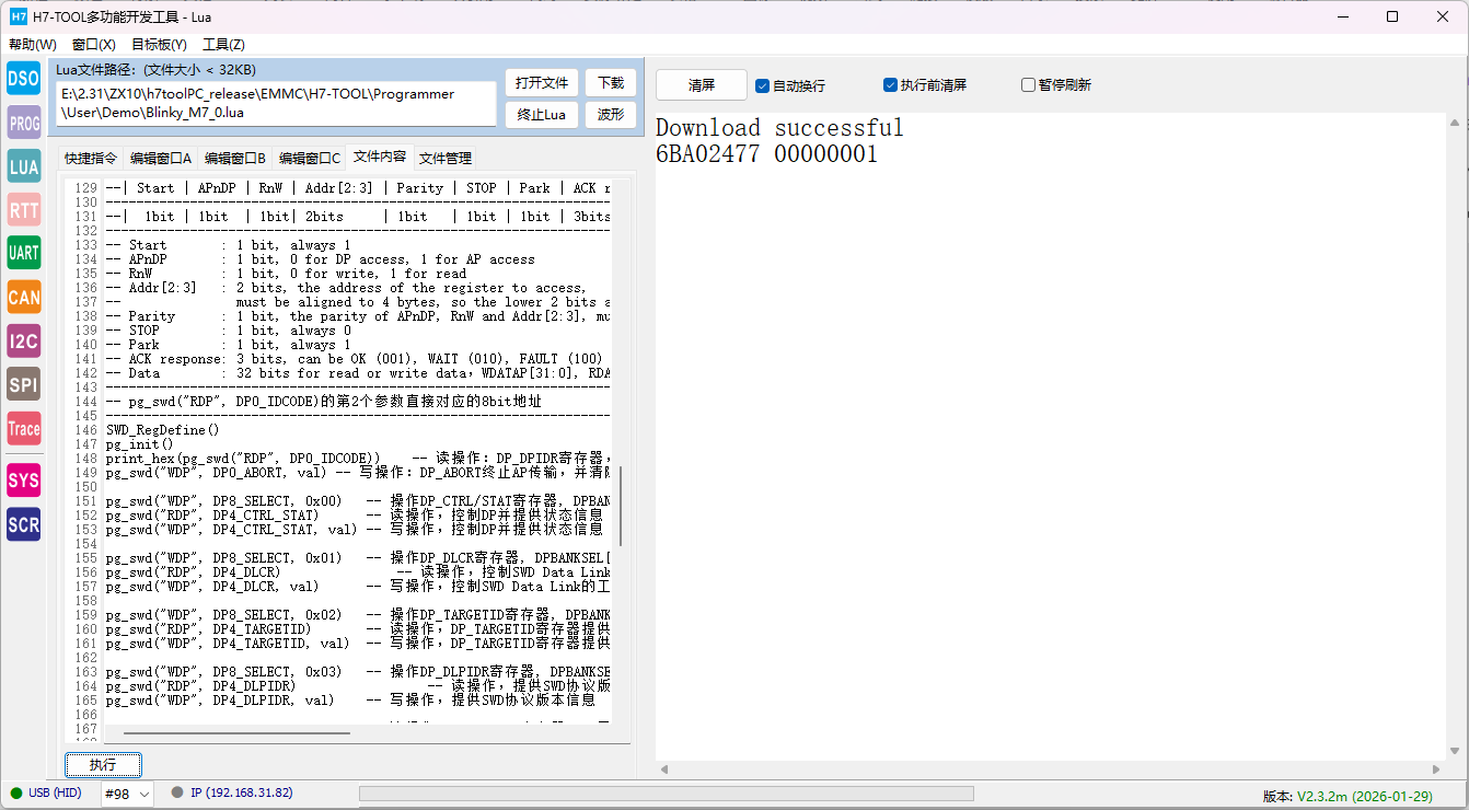
pg_swd("RDP", DP0_IDCODE) -- 读操作:DP_DPIDR寄存器,此寄存器包含了IDCODE的值
pg_swd("WDP", DP0_ABORT, val) -- 写操作:DP_ABORT终止AP传输,并清除DP_CTRL/STAT寄存器错误标志,应该是设置这个寄存器的值
pg_swd("WDP", DP8_SELECT, 0x00) -- 操作DP_CTRL/STAT寄存器, DPBANKSEL[3:0] = 0x00
pg_swd("RDP", DP4_CTRL_STAT) -- 读操作,控制DP并提供状态信息
pg_swd("WDP", DP4_CTRL_STAT, val) -- 写操作,控制DP并提供状态信息
pg_swd("WDP", DP8_SELECT, 0x01) -- 操作DP_DLCR寄存器, DPBANKSEL[3:0] = 0x01
pg_swd("RDP", DP4_DLCR) -- 读操作,控制SWD Data Link的工作模式
pg_swd("WDP", DP4_DLCR, val) -- 写操作,控制SWD Data Link的工作模式
pg_swd("WDP", DP8_SELECT, 0x02) -- 操作DP_TARGETID寄存器, DPBANKSEL[3:0] = 0x02
pg_swd("RDP", DP4_TARGETID) -- 读操作,DP_TARGETID寄存器提供目标识别信息
pg_swd("WDP", DP4_TARGETID, val) -- 写操作,DP_TARGETID寄存器提供目标识别信息
pg_swd("WDP", DP8_SELECT, 0x03) -- 操作DP_DLPIDR寄存器, DPBANKSEL[3:0] = 0x03
pg_swd("RDP", DP4_DLPIDR) -- 读操作,提供SWD协议版本信息
pg_swd("WDP", DP4_DLPIDR, val) -- 写操作,提供SWD协议版本信息
pg_swd("RDP", DP8_RESEND) -- 读操作,DP_RESEND寄存器,用于返回AP最后一次读取或者DP_RDBUFF读取,当读取传输崩溃时使用
pg_swd("WDP", DP8_SELECT, val) -- 写操作:DP_SELECT寄存器
pg_swd("RDP", DPc_RDBUFF) -- 读操作,DPc_RDBUFF寄存器,该寄存器包含前一次 AP 读取访问的结果,从而避免进行新的 AP 访问
pg_swd("WDP", DPc_TARGETSEL, val) -- 写操作:DPc_TARGETSEL寄存器选择目标设备
------------------------------------------------------------------------------------------
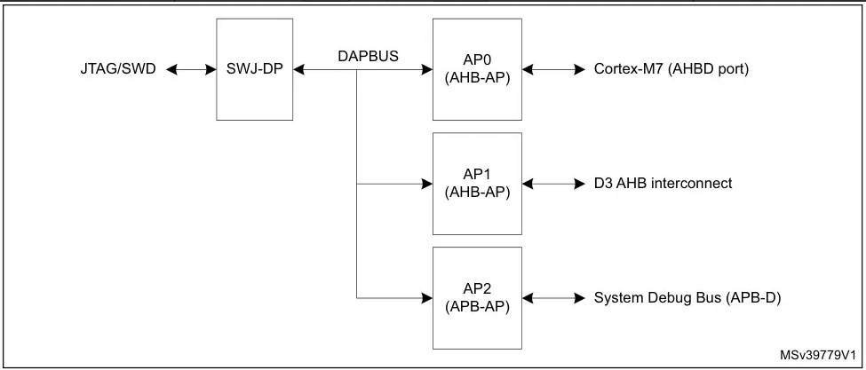
-- DP SELECT寄存器的APSEL[7:0]位选择要访问的AP,APBANKSEL[3:0]位选择要访问的AP寄存器BANK,
-- APBANKSEL支持16个BANK, 每个BANK包含4个寄存器, 由SWD Packet包的A[3:2]提供AP_A32,寄存器地址为0x00, 0x04, 0x08, 0x0C,低两个bit固定为0
-- AP Addr = (APBANKSEL << 4) | (AP_A32)
-- DP_SELECT = (APSEL << 24) | (APBANKSEL << 4)
------------------------------------------------------------------------------------------
-- pg_swd("RAP", AP0_CSW)的第2个参数直接对应的8bit地址
------------------------------------------------------------------------------------------
APSEL = 0x00 -- 赋值给DP SELECT
APBANKSEL = AP0_CSW & 0x0C -- 赋值给DP SELECT
DP_APBANKSEL = (APSEL << 24) | (APBANKSEL << 4)
pg_swd("WDP", DP8_SELECT, DP_APBANKSEL) -- 选择操作的AP端点和AP BANK
pg_swd("RAP", AP0_CSW) -- 读操作,AP0_CSW寄存器,控制和状态字寄存器
pg_swd("WAP", AP0_CSW, val) -- 写操作,AP0_CSW寄存器,控制和状态字寄存器
APSEL = 0x00 -- 赋值给DP SELECT
APBANKSEL = AP4_TAR & 0x0C -- 赋值给DP SELECT
DP_APBANKSEL = (APSEL << 24) | (APBANKSEL << 4)
pg_swd("WDP", DP8_SELECT, DP_APBANKSEL) -- 选择操作的AP端点和AP BANK
pg_swd("RAP", AP4_TAR) -- 读操作,AP4_TAR寄存器,传输地址寄存器
pg_swd("WAP", AP4_TAR, val) -- 写操作,AP4_TAR寄存器,传输地址寄存器
APSEL = 0x00 -- 赋值给DP SELECT
APBANKSEL = APc_DRW & 0x0C -- 赋值给DP SELECT
DP_APBANKSEL = (APSEL << 24) | (APBANKSEL << 4)
pg_swd("WDP", DP8_SELECT, DP_APBANKSEL) -- 选择操作的AP端点和AP BANK
pg_swd("RAP", APc_DRW) -- 读操作,APc_DRW寄存器,数据读写寄存器
pg_swd("WAP", APc_DRW, val) -- 写操作,APc_DRW寄存器,数据读写寄存器
APSEL = 0x00 -- 赋值给DP SELECT
APBANKSEL = AP10_BD0 & 0x0C -- 赋值给DP SELECT
DP_APBANKSEL = (APSEL << 24) | (APBANKSEL << 4)
pg_swd("WDP", DP8_SELECT, DP_APBANKSEL) -- 选择操作的AP端点和AP BANK
pg_swd("RAP", AP10_BD0) -- 读操作,AP10_BD0寄存器,Banked Data 0
pg_swd("WAP", AP10_BD0, val) -- 写操作,AP10_BD0寄存器,Banked Data 0
APSEL = 0x00 -- 赋值给DP SELECT
APBANKSEL = AP14_BD1 & 0x0C -- 赋值给DP SELECT
DP_APBANKSEL = (APSEL << 24) | (APBANKSEL << 4)
pg_swd("WDP", DP8_SELECT, DP_APBANKSEL) -- 选择操作的AP端点和AP BANK
pg_swd("RAP", AP14_BD1) -- 读操作,AP14_BD1寄存器,Banked Data 1
pg_swd("WAP", AP14_BD1, val) -- 写操作,AP14_BD1寄存器,Banked Data 1
APSEL = 0x00 -- 赋值给DP SELECT
APBANKSEL = AP18_BD2 & 0x0C -- 赋值给DP SELECT
DP_APBANKSEL = (APSEL << 24) | (APBANKSEL << 4)
pg_swd("WDP", DP8_SELECT, DP_APBANKSEL) -- 选择操作的AP端点和AP BANK
pg_swd("RAP", AP18_BD2) -- 读操作,AP18_BD2寄存器,Banked Data 2
pg_swd("WAP", AP18_BD2, val) -- 写操作,AP18_BD2寄存器,Banked Data 2
APSEL = 0x00 -- 赋值给DP SELECT
APBANKSEL = AP1c_BD3 & 0x0C -- 赋值给DP SELECT
DP_APBANKSEL = (APSEL << 24) | (APBANKSEL << 4)
pg_swd("WDP", DP8_SELECT, DP_APBANKSEL) -- 选择操作的AP端点和AP BANK
pg_swd("RAP", AP1c_BD3) -- 读操作,AP1c_BD3寄存器,Banked Data 3
pg_swd("WAP", AP1c_BD3, val) -- 写操作,AP1c_BD3寄存器,Banked Data 3
APSEL = 0x00 -- 赋值给DP SELECT
APBANKSEL = APf8_ROM & 0x0C -- 赋值给DP SELECT
DP_APBANKSEL = (APSEL << 24) | (APBANKSEL << 4)
pg_swd("WDP", DP8_SELECT, DP_APBANKSEL) -- 选择操作的AP端点和AP BANK
pg_swd("RAP", APf8_ROM) -- 读操作,APf8_ROM寄存器,Debug ROM Address
APSEL = 0x00 -- 赋值给DP SELECT
APBANKSEL = APfc_IDR & 0x0C -- 赋值给DP SELECT
DP_APBANKSEL = (APSEL << 24) | (APBANKSEL << 4)
pg_swd("WDP", DP8_SELECT, DP_APBANKSEL) -- 选择操作的AP端点和AP BANK
pg_swd("RAP", APfc_IDR) -- 读操作,APfc_IDR寄存器,Identification Register