How prepared RTL, disciplined compile and partitioning, debug visibility, and system-level connectivity help SoC and IP teams turn FPGA prototypes into credible pre-silicon evidence
A technical white paper from S2C Inc.
|--------------------------------------------------------------------------------------------------------------------------------------------------------------------------------------------------------------------------------------------------------------------------------------------------------------------------------------------------------------------------------------------------------------------------------------------------------------|
| Central thesis The value of an FPGA prototype is not determined by how much RTL can be loaded into FPGAs. It is determined by how quickly the team can turn ASIC RTL into a running, observable, software-connected platform that produces useful evidence before silicon: evidence that software can execute, interfaces can be exercised, failures can be observed, and project-critical questions can be answered early enough to influence outcomes. |
This paper focuses on the engineering failure modes that prevent FPGA prototypesfrom reducing tapeout risk: ASIC-specific RTL structures, uncontrolled compile iteration, late partitioning analysis, limited debug visibility, weak host connectivity, and ad hoc interface infrastructure. It then maps those risks to the elements of S2C's Prodigy prototyping environment: Logic System, Logic Matrix, Player Pro, MDM Pro, ProtoBridge, Prototype Ready IP, and Neuro.
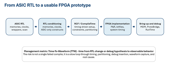
Figure 1. From RTL fit to useful pre-silicon evidence: prepared RTL, disciplined implementation, planned debug, and system connectivity must work together.
Executive summary
FPGA prototypingremains one of the highest-value pre-silicon validation methods because it can run real RTL fast enough for firmware, drivers, OS boot, hardware/software co-validation, and system-level traffic that would be impractical in pure simulation. The challenge is that modern SoCs are too large, too clock-complex, too software-dependent, and too interface-rich for a board-only strategy.
A prototype that compiles but arrives too late, runs too slowly, exposes too little internal state, or cannot connect to the software and I/O environment does not reduce tapeout risk. It becomes another engineering artifact to debug. The management objective should be to create a prototype that can answer project-critical questions before tapeout.
For most SoC teams, the practical question is not simply, 'How many FPGAs do we need?' The better question is, 'How fast can we convert ASIC RTL into a running, observable, interface-connected validation platform, and how quickly can we iterate when it fails?' That shift moves the discussion from RTL fit to useful pre-silicon evidence.
This paper is written for engineering leaders and senior validation teams who need FPGA prototyping to do more than demonstrate RTL fit. The goal is to create a platform that can answer schedule-critical questions before tapeout: Can software run? Can interfaces be exercised? Can failures be observed? Can the team iterate fast enough to change outcomes?
S2C's Prodigy environment addresses this problem as a workflow, not only as hardware capacity. Logic System and Logic Matrix provide the scalable FPGA platform; Player Pro and RCF help manage compile, partitioning, timing, and iteration; MDM Pro preserves debug visibility; ProtoBridge and Prototype Ready IP connect the prototype to software and real interfaces; and Neuro supports shared prototyping resources across teams.
From RTL fit to useful pre-silicon evidence
A useful prototype creates several kinds of evidence that matter to different teams. The architecture should be selected and managed around those evidence goals, not capacity alone.
|------------------------------------------|--------------------------------------------------------------------------------------------------|
| Evidence the prototype should produce | Why it matters before silicon |
| RTL can execute in a system context | Confirms that prepared RTL, clocks, memories, and partitioning can support meaningful execution. |
| Firmware, drivers, or OS flows can run | Lets software teams begin controlled bring-up and error-handling work before first silicon. |
| Critical interfaces can move traffic | Exposes integration, protocol, and I/O behavior that may not appear in block-level simulation. |
| Failures can be observed and root-caused | Reduces the risk that the prototype runs but cannot explain incorrect behavior. |
| Validation assets can be reused | Improves continuity from prototype bring-up to first-silicon readiness and future programs. |
Prototype objectives should be defined before architecture selection
The requirements for a useful prototype depend on the evidence the team needs to create. A platform sized only for RTL fit may still miss the needs of firmware, driver, system-validation, or customer-enablement teams.
|----------------------------------|-------------------------------------------------------------------------------------------------------------------------------------|
| Prototype objective | What the platform must support |
| Firmware or OS boot | Stable reset and clock behavior, memory access, interrupt delivery, and enough execution speed to make software iteration practical |
| Driver development | Register access, host-driven transactions, interface behavior, and repeatable error-handling scenarios |
| System validation | Long-running workloads, realistic traffic, external I/O paths, and debug capture across relevant blocks |
| Customer or ecosystem enablement | A repeatable demo environment that exposes intended features without depending on first silicon |
| Post-silicon readiness | Reusable software flows and test content that can transfer into first-silicon bring-up |
Where prototyping programs usually lose time
|-----------------------------------------------------|--------------------------------------------------------------------------------------------------------------------------------------------------------------------------------|
| Failure mode | Typical project impact |
| ASIC RTL pushed directly into FPGA implementation | * Synthesis instability, inefficient resource mapping, unexpected timing failures |
| Poor memory or clock preparation | * A prototype that compiles late, runs slowly, or differs from ASIC intent |
| Partitioning treated as a rescue step | * Cross-FPGA bandwidth, latency, and timing problems discovered too late |
| Debug planned after bring-up | * Long root-cause cycles and repeated recompiles to expose signals |
| No host or interface strategy | * Prototype cannot support firmware, driver, or system traffic milestones |
| One-off infrastructure | * Useful assets are not reused across SoC/IP programs |
| ASIC gate count used as the capacity proxy | * Prototype sizing is wrong because LUTs, registers, memories, DSPs, I/O, debug logic, and routing congestion do not scale from gate count in a fixed ratio |
| ASIC constraints copied without FPGA interpretation | * Timing reports become misleading, and teams spend iterations chasing constraints that do not match FPGA clocks, generated clocks, inter-FPGA links, or validation objectives |
| Utilization headroom ignored | * The design may appear to fit but leave too little routing, memory, or logic margin for debug probes, wrappers, pin multiplexing, interface logic, and late ECOs |
The urgency is increasing as SoCs carry more software-visible functionality, more external interfaces, and more subsystem-level integration risk. Simulation and emulation remain essential, but many teams still need an FPGA-based platform that can run long workloads, connect to real software environments, and expose system behavior early enough to influence the project.
The rest of this paper uses those failure modes as the organizing framework.
1. Prepared RTL is the first gating item
Capacity is visible, but RTL readiness is often the first practical failure point. ASIC RTL usually contains implementation assumptions that are valid for standard-cell design but hostile to FPGA fabric: compiled SRAM macros, custom register files, gated clocks, clock muxing, scan-related structures, technology-specific wrappers, and reset behavior tied to an ASIC methodology.
When this RTL is taken directly into an FPGA implementation flow, the tool chain must infer intent from structures that were not written for FPGA architecture. The symptoms are familiar: synthesis exceptions, poor mapping, excessive congestion, unstable timing, low operating frequency, and repeated manual edits to get from compile to first useful waveform.
ASIC-to-FPGA is not a direct port
The same RTL can be functionally correct for ASIC implementation and still be poorly suited for FPGA prototyping. Encrypted or technology-specific IP, arithmetic/DSP macros, scan/test wrappers, unsupported primitives, generated clocks, high-fanout control nets, and reset assumptions can all affect compile success, achievable frequency, and debug visibility.
The implication for engineering management is simple: early FPGA-readiness analysis is not overhead. It is the work that prevents the prototype from becoming a late-stage debugging exercise around clocks, memories, constraints, and resource mapping.
Memory mapping and clocking are high-leverage examples
Memory macro replacement is not a mechanical bit-count exercise. ASIC SRAMs and register files often differ from FPGA BRAM, URAM, distributed RAM, or external-memory models in port count, banking, aspect ratio, reset behavior, collision semantics, and latency assumptions. A naive replacement can create unnecessary congestion or functional divergence from the ASIC intent.
Clock gating has the same issue. ASIC clock-gating cells are designed for a controlled clock-tree synthesis environment. In an FPGA prototype, gated clocks and clock muxes should usually be translated into FPGA-suitable clock enables, clock-buffer structures, or constrained clocking schemes that preserve the design intent without recreating ASIC clock trees in FPGA routing.
The important point is not that every transformation belongs to one tool. The point is that these issues must be addressed deliberately before partitioning and timing closure are treated as final implementation problems.
Partitioning is necessary, but it is not the starting point
Large SoCs often require multiple FPGAs. That makes partitioning unavoidable, and it is one of the most visible parts of the prototyping flow. However, partitioning does not repair unprepared RTL. It exposes the consequences of unprepared RTL across device boundaries.
Multi-FPGA partitioning introduces real costs: inter-FPGA latency, limited pin bandwidth, serialization overhead, additional timing margins, and constraints around high-fanout nets and clock-domain crossings. The prototype architecture should therefore be planned around software milestones, debug visibility, I/O needs, and achievable frequency - not just LUT capacity.
Capacity planning must include margin and constraints
ASIC gate count is a weak proxy for FPGA capacity. The usable size of a prototype depends on the LUT/register mix, memory aspect ratios, DSP use, I/O, clocking, partition overhead, probe insertion, and routing congestion. Early synthesis or estimation against the target FPGA family is more useful than relying on a fixed gate-count multiplier.
Utilization headroom should also be treated as part of the architecture. A design that consumes most of the available FPGA fabric may leave too little margin for debug, wrappers, pin multiplexing, interface adapters, or ECOs, and may produce long or inconsistent place-and-route iterations.
Constraint translation is another early task. ASIC constraints cannot be blindly copied into the FPGA flow. SDC/XDC constraints need to reflect FPGA clock resources, generated clocks, false and multicycle paths, I/O timing, debug insertion, and inter-FPGA links.
2. Reduce Time-To-Waveform, not just compile time
Once the RTL is prepared, the next executive-level risk is iteration speed. The relevant metric is not only first compile or maximum MHz. A more useful metric is Time-To-Waveform: the time from an RTL change or debug hypothesis to observable behavior on the running prototype.
For large SoC programs, schedule is often lost not in one failed compile, but in repeated loops between hypothesis, implementation, execution, capture, and analysis. Time-To-Waveform makes that loop visible. Reducing it can directly improve how quickly teams find bugs, validate fixes, and restore confidence in the prototype.
This is where S2C's RTL Compile Flow (RCF) material strengthens the story. RCF is described as enabling customization of timing-driven and congestion-aware synthesis and technology mapping for individual FPGAs, supporting an SDC-based timing-closure flow, and using incremental compile and debug flow to reduce TTW. It also emphasizes an RTL-level database for compile efficiency and access to original DUT RTL signals for debug.
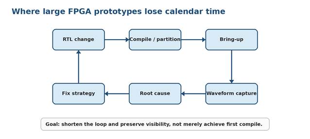
Figure 2. Time-To-Waveform focuses management attention on the repeated engineering loop, not only the duration of one implementation run.
Compile and partitioning discipline belong in the prototyping architecture
S2C's Player Pro helps teams manage the repeated loops that determine prototype schedule. CompileTime handles prototype configuration, automatic and guided partitioning, enhanced partitioning/TDM macros, system timing reporting, modular replicate, and incremental compile. RunTime manages remote system operation, and DebugTime supports multi-FPGA debug setup.
That matters because large prototypes rarely fail through a single event. They lose schedule through repeated loops: timing closure, partition changes, pin multiplexing, debug setup, waveform capture, RTL edits, and recompile. A disciplined compile environment should make that loop shorter, more repeatable, and more visible to the engineering manager.
3. Debug visibility is a platform requirement
Debug should not be treated as a late-stage add-on after the design fits. If important signals cannot be observed without disruptive recompilation, the prototype may run but still fail to support root-cause analysis. This is especially true in multi-FPGA systems, where a failure may involve transactions crossing device boundaries, clocks, memories, and external interfaces.
Embedded FPGA logic analyzers are useful, but they are not free. Probe logic, trace buffers, and routing can consume LUTs, block RAM, and timing margin. On large prototypes, debug infrastructure can become the factor that determines whether the team can observe the right behavior without another long compile cycle.
S2C's MDM Pro is relevant because debug visibility determines whether a running prototype can actually explain system behavior. The public product page describes deep-trace debugging across multiple FPGAs, tracing large numbers of signals per FPGA without recompile in supported configurations, external waveform storage, hardware trigger support, and single-window multi-FPGA debug. The practical value is not just more probes; it is better continuity between hypothesis, capture, and root cause.
Debug planning changes the compile strategy
Good debug planning starts before bring-up. Teams should identify which buses, state machines, clock/reset controls, interface boundaries, and software-visible registers must remain observable. That decision affects RTL conditioning, partitioning, probe insertion, waveform storage, and the acceptable TTW for each bring-up milestone.
This is also where the RCF point about original DUT RTL signal visibility matters. For hardware teams, debug is easier when signals are still recognizable from the RTL source rather than buried behind implementation-specific names and transformations.
4. The prototype must connect to software and real interfaces
A useful prototype has to serve more than the RTL team. Firmware engineers need to boot, configure, and exercise the design. Driver teams need register access and traffic. System teams need realistic I/O paths. Business leaders may need a demonstrable platform for partners, early customers, or investors. None of that is delivered by FPGA capacity alone.
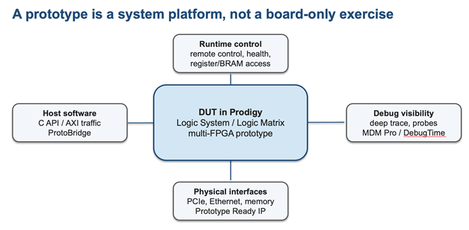
Figure 3. System-level value comes from the combination of the DUT, debug, host access, runtime control, and reusable I/O infrastructure.
Host-to-DUT access turns the prototype into a software instrument
ProtoBridge is a strong part of the S2C story because it connects the FPGA prototype to host software using AXI-4 transaction-level access and C-API calls. In practical terms, this lets teams configure registers, inject transactions, move data, and build host-driven test environments without treating the prototype as an isolated hardware box.
For software and firmware teams, this matters because the early value of a prototype is often in controlled interaction: configure the design, run real traffic, check state, isolate a failure, adjust the workload, and repeat. That is difficult if every test requires custom bench work or manual board-level intervention.
Reusable interface infrastructure reduces calendar variance
External interfaces are frequent sources of schedule risk. PCIe, Ethernet, USB, MIPI, memory, storage, and other I/O paths all have board-level, protocol, and software dependencies. S2C's Prototype Ready IP and daughter-card library address this problem by providing reusable interface hardware and reference design flows that can be applied across programs.
Interface planning should also consider how the prototype will be used outside the core RTL team. Some programs need to connect to previous-generation platforms, external peripherals, traffic generators, or customer application cards. Those requirements should be captured before partitioning and board bring-up decisions are locked.
For engineering executives, the point is repeatability. A team that reuses known-good boards, interface cards, host APIs, and bring-up steps is less exposed to one-off infrastructure delays. A team that starts each prototype from custom wiring and custom software spends schedule on infrastructure rather than product validation.
5. How the S2C platform maps to the workflow
The cleanest way to describe S2C is by workflow role, not by listing product names. The Prodigy environment is best understood as an integrated platform for converting ASIC RTL into an executable, debuggable, connected prototype.
|--------------------------------------|----------------------------------------------|-----------------------------------------------------------------------------------------------------------|
| Workflow need | S2C platform element | Why it matters |
| Scalable FPGA capacity | Prodigy Logic System / Logic Matrix | Supports subsystem, full-chip, and larger multi-FPGA deployments |
| Compile, partitioning, runtime setup | Player Pro: CompileTime, RunTime, DebugTime | Controls the implementation loop around partitioning, timing reports, debug setup, and system operation |
| Compile iteration and RTL visibility | RTL Compile Flow / RCF | Targets timing/congestion-aware mapping, SDC-driven iteration, incremental compile/debug, and reduced TTW |
| Multi-FPGA observability | MDM Pro | Supports deeper debug capture across FPGAs with external storage and advanced trigger capability |
| Host-driven validation | ProtoBridge | Provides AXI-4 transaction-level host-to-DUT connectivity using C-API calls |
| Physical I/O and reuse | Daughter Cards / Memory Model / Speed Bridge | Reduces custom interface bring-up with pre-tested cards, integrated rate adaptation, and reference flows |
| Fleet and resource management | Neuro | Supports resource management for larger shared prototyping environments |
6. Modular SoC and chiplet-oriented designs make the planning problem clearer
Chiplet architecture should not be presented as an S2C-specific claim. It is an industry trend that changes how teams think about validation boundaries. From a prototyping perspective, the useful point is that smaller, better-defined subsystem or die-level boundaries can sometimes map more naturally into FPGA-based validation environments than a monolithic full-chip cut.
For chiplet programs, the interconnect becomes a first-class validation target. Latency, ordering, flow control, reset behavior, error handling, coherency interactions, firmware control, and software-visible configuration all need to be exercised before packaging and silicon are committed. FPGA prototyping cannot replace signal-integrity, package, or PHY validation, but it can help validate protocol behavior, software interaction, and system traffic earlier.
The best prototype strategy often follows the same boundaries as the product architecture: validate IP blocks, validate subsystem integration, validate interconnect behavior, then connect enough of the platform to support software milestones.
7. Prototype readiness checklist: is the platform ready to reduce tapeout risk?
Use these questions to determine whether the prototype is ready to produce useful pre-silicon evidence, or whether it is only sized to fit RTL. They should be answered before a team commits to a prototyping architecture or treats first compile as the main milestone.
- What software milestone must the prototype support: firmware smoke test, driver bring-up, OS boot, workload execution, customer demo, or system validation?
- What minimum operating frequency is required for each milestone?
- Which ASIC memories need replacement, modeling, black-box treatment, or external-memory mapping?
- Which gated clocks, clock muxes, resets, and clock-domain crossings must be converted, constrained, or isolated?
- Which signals cross FPGA boundaries, and what latency/bandwidth can those crossings tolerate?
- Which debug signals must remain visible without full recompile?
- What is the acceptable Time-To-Waveform for bring-up and root-cause work?
- Which physical interfaces require daughter cards, speed bridges, transactors, or host-driven access?
- Which assets can be reused across programs: boards, cards, reference designs, APIs, debug setup, scripts, or runtime control?
- Has FPGA fit been estimated with early synthesis or resource analysis rather than ASIC gate count alone?
- What utilization margin is reserved for debug probes, interface wrappers, pin multiplexing, timing optimization, and late ECOs?
- How will ASIC constraints be translated into FPGA constraints for generated clocks, false paths, multicycle paths, I/O timing, and inter-FPGA links?
- Which encrypted IP, technology-specific macros, or implementation wrappers require replacement, black-boxing, or alternate synthesis treatment?
|---------------------------------------------------------------------------------------------------------------------------------------------------------------------------------------------------------------------------|
| SoC customer perspective Approved quote on reducing compile/debug iteration time, improving RTL visibility, or making software bring-up practical before silicon. |
| IP supplier perspective Approved quote on using FPGA prototypes to help customers integrate IP, exercise drivers, validate interfaces, or reproduce system-level behavior before the customer SoC is available. |
Conclusion
FPGA prototyping continues to matter because it can expose system behavior before silicon and at speeds that are useful for firmware, drivers, and real traffic. The limitation is that modern SoCs are too large and too ASIC-specific for a board-only strategy.
The stronger prototyping strategy starts earlier. It prepares ASIC RTL for FPGA implementation, treats compile iteration as a management issue, plans partitioning before it becomes a rescue operation, preserves debug visibility, connects the prototype to host software and real interfaces, and reuses known-good infrastructure across programs.
It also treats resource planning, constraint translation, and debug capacity as first-order architecture decisions rather than late implementation details.
For S2C, the strongest message is not simply high FPGA capacity. It is a complete Prodigy environment that helps SoC and IP teams move from RTL fit to useful pre-silicon evidence: a running, observable, software-connected platform that can answer project-critical questions before silicon.
Next step: validate more than FPGA capacity
Before committing to a prototyping architecture, validate more than FPGA capacity. SoC and IP teams should understand how the design will map into FPGA resources, where partitioning may be required, which interfaces need physical connectivity, what debug visibility must be preserved, and how software and RTL teams will interact with the system once it is running.
S2C can help engineering teams assess RTL readiness, partitioning risk, debug strategy, host connectivity, interface requirements, utilization margin, and reuse opportunities --- so the prototype is planned as a working pre-silicon validation platform, not just a board-level implementation target.
Visit the S2C website to learn more and schedule a technical discussion or platform demonstration for your next ASIC, SoC, or IP validation program.