1、J-linK介绍
J-Link是由德国SEGGER公司推出的,主要用于支持仿真ARM内核芯片的JTAG仿真器。它支持JTAG和SWD两种模式,可以配合多种集成开发环境(如IAR EWAR, ADS, KEIL, WINARM, RealView等)使用,支持ARM7/ARM9/ARM11, Cortex M0/M1/M3/M4, Cortex A5/A8/A9等内核芯片的仿真。J-Link的驱动和固件版本可能会影响读取hex文件的结果,因为不同的固件版本和读取设置可能会导致细微的差异。
2、烧录
本文是通过J-Link V7.6版本进行烧录hex固件
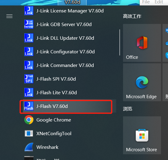
1、打开JFlash
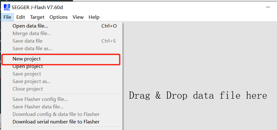
2、创建新工程
点击File->New project
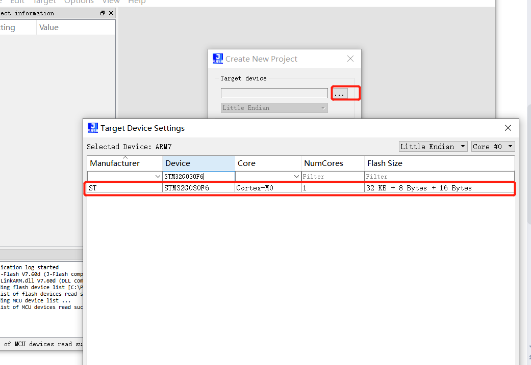
3、选择芯片型号
择要读取/写入单片机对应的芯片型号,我这里选择的是STM32G030F6系列,选择的SWD模式。
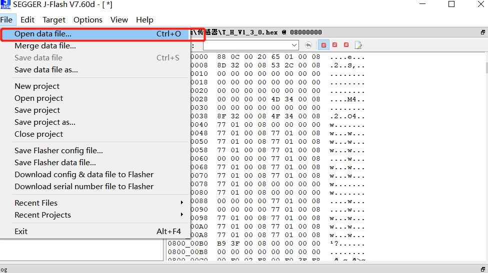
4、打开程序
点击File->Open data file,选择烧录程序文件。
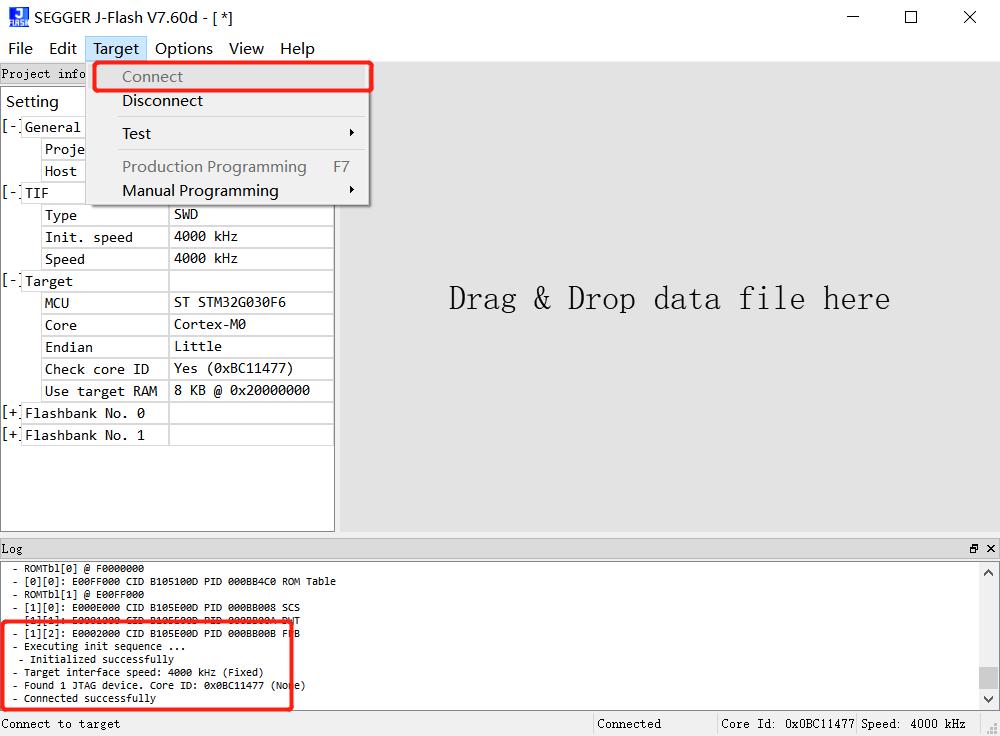
5、连接芯片
连接SWDIO、SWCLK、GND这三根线,连接好之后,点击Target->Connect,如果连接成功,在下面的LOG窗口会显示连接成功
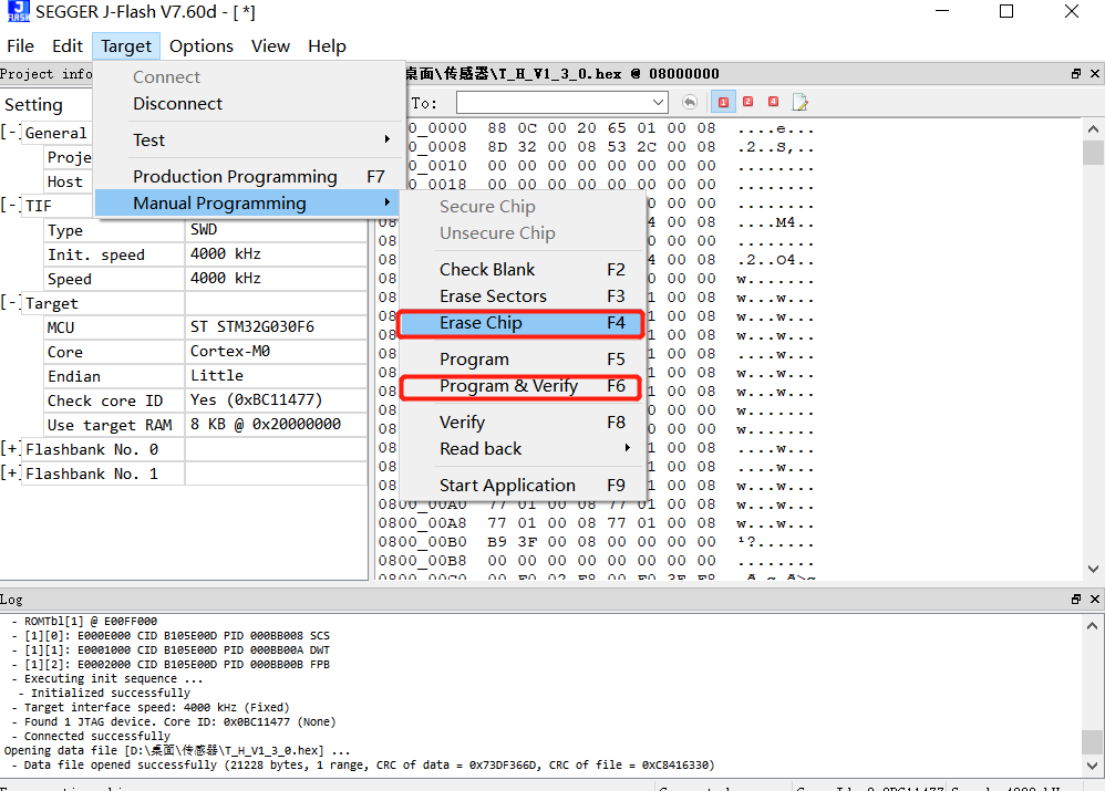
6、程序写入
选择Target->Manual Programming->Erase chip清空单片机里面的程序,
清空之后选择Program&Verify进行烧录程序。
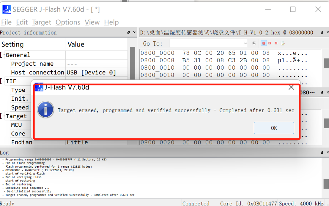
当弹出这个弹窗的时候,表示烧录成功。
3、问题与解决
可能出现的问题:
JLINK烧写程序遇到的常见错误ERROR:RAM check failed @ADDRESS 0x20000000
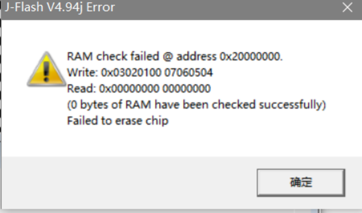
该问题主要是供电问题,查看电路板供电是否正常