Solder powder is an indispensable connecting material in the electronics industry, mainly used to formulate solder paste for the soldering process of surface mount technology (SMT). The quality of the solder powder directly affects the performance of the solder paste and the welding quality of the circuit board, so the preparation process of the solder powder has high requirements. At present, the commonly used solder powder preparation process has a gas atomization method, rotating disk centrifugal atomization method and ultrasonic atomization method, etc., of which the ultrasonic atomization method has been used to produce high-quality solder powder used for soldering and solder paste, is currently the mainstream of the European and American countries to make the ultra-fine powder process.
The principle of ultrasonic atomization method is the use of ultrasound vibration and cavitation effect, the molten metal droplets in the ultrasonic transducer atomized into tiny droplets, and cooled in the air to solidify into spherical powder particles. The ultrasonic transducer is the core component of the whole system, which converts the high-frequency electrical signal into mechanical vibration of the same frequency, and amplifies its amplitude through the amplifier rod to drive the atomization angle end face for ultrasonic vibration. The molten metal liquid is transported to the top of the atomizing angle through the guide tube, and due to the ultrasonic effect, the metal liquid is broken into tiny droplets and drifts down with the airflow. In the process of falling, the droplets rapidly cool and solidify to form spherical powder particles, which are collected in the powder collecting cylinder.
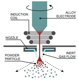
Figure 1. Principle of ultrasonic atomization method
The characteristics and advantages of the ultrasonic atomization method of preparing solder powder are as follows:
-
The morphology and size of the powder particles can be controlled, so as to obtain highly spherical, uniform particle size and narrow distribution of the powder.
-
The purity and oxygen content of the powder particles are low, and in the ultrasonic atomization process, the contact area between the metal liquid and the gas is small, and the degree of oxidation is low, and it can be atomized in an inert atmosphere to further reduce the possibility of oxidation.
-
Simple equipment and process, convenient operation, stable and controllable product quality.
-
Small energy consumption, high utilization rate, low cost, environmental protection and energy saving.
Although the ultrasonic atomization process for the production of solder powder has a series of advantages, but the ultrasonic atomization process yield is small, the capacity can not meet the market demand, so manufacturers in the mass production of T6 below the conventional solder powder generally use centrifugal atomization process.
In order to solve the problem of low yield in the production of ultra-fine powder above T6, Shenzhen Fuyinda company independently developed a unique alloy powder preparation technology - liquid phase molding preparation technology, the use of the principle of ultrasonic cavitation effect, the preparation of ultra-fine solder powder above T6, the production of solder powder powder powder not only has a good shape of ultrasonic atomization process has Its production of welding powder powder not only has the advantages of good morphology, uniform and controllable particle size, low oxygen content, etc., but also solves the problem of insufficient production capacity, and has realized large-scale mass production.
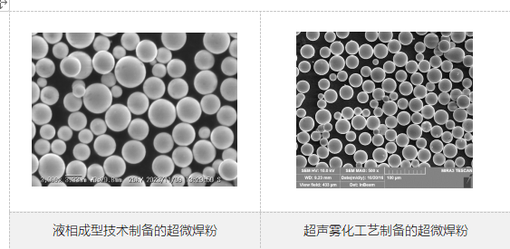
Figure 2: Comparison of the morphology of solder powder prepared by liquid phase forming technology and ultrasonic atomization process.