FPGA Prototyping vs. Emulation
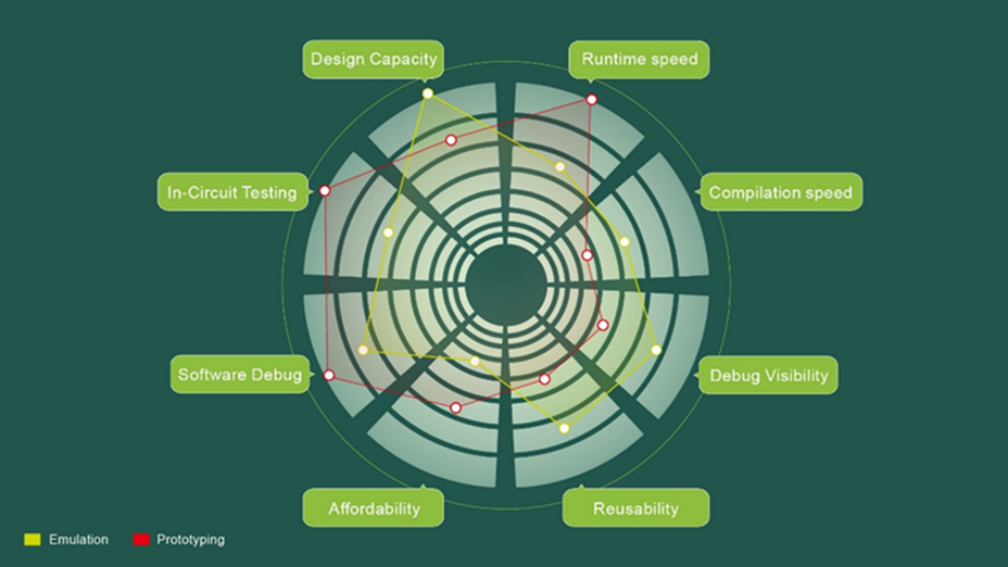
One way to visualize the difference between Prototyping and Emulation is with a "spider chart" (named for its resemblance to a spider's web). The Prototyping vs. Emulation spider chart below highlights the differences between these two verification methods, which may be summarized as runtime speed, design capacity, and affordability -- all other differences, sometimes not insignificant, are "artifacts" of these three fundamental differences. Compilation speed is a function of design capacity -- the larger the design the longer the compilation time. Any simulator can be connected in-circuit to a hardware target system with the appropriate speed-buffers but the verification runtime speed is still limited by the simulation platform -- Emulation runtime speed is much faster than software simulation, and achievable Prototyping runtime speeds are much higher than Emulation runtime speeds. Likewise, any simulator can be used for software debug for periods of software execution -- the higher runtime speeds of Prototyping enable much longer periods of software execution therefor longer software debug sessions. And debug visibility could include every internal design node in a Prototype or Emulator -- but each design node probe is another internal wire connection in FPGA-based Prototyping and Emulation implementations, which impacts design capacity and runtime speed. Finally, reusability is a function of the customization of the Prototyping or Emulation platform needed to achieve the verification design capacity and runtime speed goals -- the more customized the platform is for the specific verification requirements, the less reusable it will be. The underlying Prototyping or Emulation hardware itself is infinitely reusable, but the design compilations, IP block adaptations, and external connections will have limited reusability.
What Can FPGA Prototyping or Emulation Do Best for You?
To summarize, FPGA Prototyping today is generally more affordable than Emulation, it can achieve much higher runtime speeds, and design capacity has been greatly expanded by today's leading-edge FPGA technology. Emulation, on the other hand comes with a higher cost of ownership, provides more simulation-like verification for design debug. In fact, if you can afford both Prototyping and Emulation, debug with Prototyping is usually limited to identifying and isolating design hardware/software problems over long periods of design operation which are then reproduced in Emulation for detailed debug. It is recommended that you be clear about your verification goals and priorities, you consider the skill set of your design team with respect to getting the best value from Prototyping and/or Emulation, do a quick ROI calculation on your verification tool investment, budget accordingly -- and only then proceed with a choice and deployment of FPGA Prototyping and/or Emulation.
S2C Can Help
S2C is a leading global supplier of FPGA prototyping solutions for today's innovative SoC and ASIC designs, now with the second largest share of the global prototyping market. S2C has been successfully delivering rapid SoC prototyping solutions since 2003. With over 500 customers, including 6 of the world's top 15 semiconductor companies, our world-class engineering team and customer-centric sales team are experts at addressing our customer's SoC and ASIC verification needs. S2C has offices and sales representatives in the US, Europe, mainland China, Hong Kong, Korea, and Japan.