目录
[1、SYSTEM CORE](#1、SYSTEM CORE)
[2、TRACE AND DEBUG](#2、TRACE AND DEBUG)
[4、Code Generator](#4、Code Generator)
[(1)查询NAND FLASH的参数](#(1)查询NAND FLASH的参数)
[(3)调用HAL函数对NAND FLASH进行访问](#(3)调用HAL函数对NAND FLASH进行访问)
本文通过实例旨在进一步介绍STM32H743单片机通过FMC扩展NAND FLASH的方法。本文作者通过编写NAND FLASH的驱动,实现了NAND_AddressTypeDef实例的逻辑盘符与物理地址的映射方法。进一步地,通过此驱动,本文可以放心确认逻辑盘符的编号只在同一个block里连续排列,跨block时,逻辑page编号从0开始重新排列。
通过这样的驱动定义,NAND_AddressTypeDef实例的含义一目了然,便于读者和编程人员阅读和理解。比如:NAND_AddressTypeDef addr ={0,0,0}代表page0,plane0,block0;{63,0,1023}代表page63,plane0,block1023;{63,0,1000}代表page63,plane0,block1000;虽然page的编号都是63,但是前者是block1023的page63,后者是block1000的page63。依此类推。
为了更好地理解本文所述内容,可以参考本文作者写的其他本章,参考文章:
细说STM32F407单片机通过FSMC访问片外NAND Flash的方法及实例_mcu移植nand flash-CSDN博客 https://wenchm.blog.csdn.net/article/details/155067571?spm=1011.2415.3001.5331
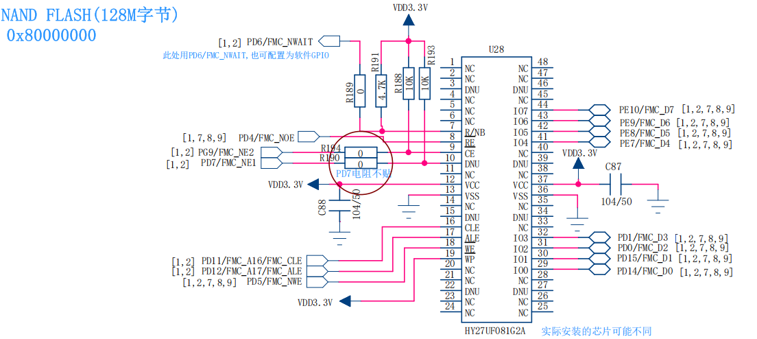
本文使用安富莱的开发板,STM32-V7;核心板MCU,STM32H743XIH6;核心板载的NAND FLASH:HY27UF081G2A=(2K+64)bytes*1024blocks*1plane;原理图:
本文开发环境使用STM32CubeIDE Version: 1.19.0;
一、工程配置
1、SYSTEM CORE
(1)RCC
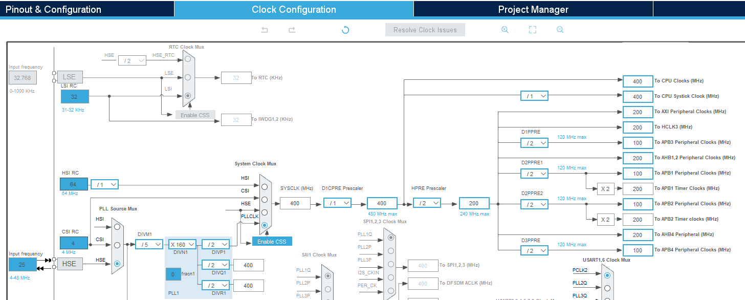
HSE外部晶振,25MHz。
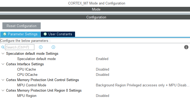
(2)CORTEX_M7
禁用I_Cache和D_Cache。
(3)NVIC
修改timebase中断为0,其余默认;
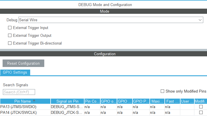
2、TRACE AND DEBUG
选择serial wire。
3、Connectivity
(1)USART1
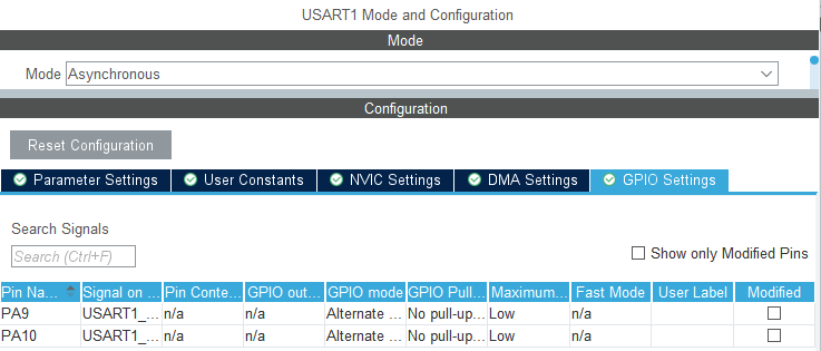
参数选择默认;
(2)FMC
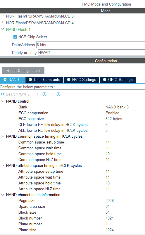
其中,
cpp
TCLRSetupTime=tCLR/tHCLK=15/5=3;
TARSetupTime =tAR/tHCLK=15/5=3;
其中的common space timing in HCLK cycles和attribute space timing in HCLK cycles等8个参数,按照参考文章提供的方法试算,试算的结果不一定符合要求,但接近目标的要求,多测试几次,就会摸索到最合适的参数了。
其中,characteristic infomation按照NAND FLASH数据手册填写。
4、Code Generator

二、软件设计
编译、IDE自动生成驱动。
1、nand_flash.h/.c
这个驱动是本文最大的创新点和贡献。其方法思路是:
(1)先计算FLASH的物理页地址
cpp
/* USER CODE BEGIN PRIVATE_DEFINES */
/* @brief 	K9F1G08U0B,128M x 8 Bit NAND Flash Memory,
 * 			total 128M bytes used to USBD MSC
 * 			1 Page	= (2048+64)Bytes
 * 			1 Block	= (2048+64)Bytes x 64 Pages
 *					= (128K + 4K)Bytes
 *			1 Device= (128K + 4K)Bytes x 1024 Blocks
 *					= (128M + 4M)Bytes
 */

/* FSMC Nand Flash Base address. */
#define NAND_FLASH_BASE NAND_DEVICE

/* NAND FLASH PHYSIC LUN BASE ADDRESS*/
#define FLASH_PAGE_BASE		((uint32_t)NAND_FLASH_BASE)
#define FLASH_BLOCKE_BASE	((uint32_t)NAND_FLASH_BASE)
#define FLASH_PLANE_BASE	((uint32_t)NAND_FLASH_BASE)


/**
 * @brief Calculte physics address.
 */
/* Base physics address of the Nand Flash pages. */
#define ADDR_FLASH_PAGE_0	((uint32_t)(FLASH_PAGE_BASE + 0x0)) /* Base @ of Page0, 2 Kbyte */
#define ADDR_FLASH_PAGE_1	((uint32_t)(FLASH_PAGE_BASE + 0x800)) /* Base @ of Page1, 2 Kbyte */
#define ADDR_FLASH_PAGE_2	((uint32_t)(FLASH_PAGE_BASE + 0x1000)) /* Base @ of Page2, 2 Kbyte */
#define ADDR_FLASH_PAGE_3	((uint32_t)(FLASH_PAGE_BASE + 0x1800)) /* Base @ of Page3, 2 Kbyte */
#define ADDR_FLASH_PAGE_4	((uint32_t)(FLASH_PAGE_BASE + 0x2000)) /* Base @ of Page4, 2 Kbyte */
#define ADDR_FLASH_PAGE_5	((uint32_t)(FLASH_PAGE_BASE + 0x2800)) /* Base @ of Page5, 2 Kbyte */

...  ....
//省去中间众多宏定义
... ....

#define ADDR_FLASH_PAGE_65528	((uint32_t)(FLASH_PAGE_BASE + 0x7ffc000)) /* Base @ of Page65528, 2 Kbyte */
#define ADDR_FLASH_PAGE_65529	((uint32_t)(FLASH_PAGE_BASE + 0x7ffc800)) /* Base @ of Page65529, 2 Kbyte */
#define ADDR_FLASH_PAGE_65530	((uint32_t)(FLASH_PAGE_BASE + 0x7ffd000)) /* Base @ of Page65530, 2 Kbyte */
#define ADDR_FLASH_PAGE_65531	((uint32_t)(FLASH_PAGE_BASE + 0x7ffd800)) /* Base @ of Page65531, 2 Kbyte */
#define ADDR_FLASH_PAGE_65532	((uint32_t)(FLASH_PAGE_BASE + 0x7ffe000)) /* Base @ of Page65532, 2 Kbyte */
#define ADDR_FLASH_PAGE_65533	((uint32_t)(FLASH_PAGE_BASE + 0x7ffe800)) /* Base @ of Page65533, 2 Kbyte */
#define ADDR_FLASH_PAGE_65534	((uint32_t)(FLASH_PAGE_BASE + 0x7fff000)) /* Base @ of Page65534, 2 Kbyte */
#define ADDR_FLASH_PAGE_65535	((uint32_t)(FLASH_PAGE_BASE + 0x7fff800)) /* Base @ of Page65535, 2 Kbyte */
(2)再计算FLASH的物理块地址
cpp
/* Base physics address of the Nand Flash blocks. */
#define ADDR_FLASH_BLOCK_0	((uint32_t)(FLASH_BLOCKE_BASE + 0x0)) /* Base @ of Block0, 128Kbyte */
#define ADDR_FLASH_BLOCK_1	((uint32_t)(FLASH_BLOCKE_BASE + 0x20000)) /* Base @ of Block1, 128Kbyte */
#define ADDR_FLASH_BLOCK_2	((uint32_t)(FLASH_BLOCKE_BASE + 0x40000)) /* Base @ of Block2, 128Kbyte */
#define ADDR_FLASH_BLOCK_3	((uint32_t)(FLASH_BLOCKE_BASE + 0x60000)) /* Base @ of Block3, 128Kbyte */
#define ADDR_FLASH_BLOCK_4	((uint32_t)(FLASH_BLOCKE_BASE + 0x80000)) /* Base @ of Block4, 128Kbyte */
#define ADDR_FLASH_BLOCK_5	((uint32_t)(FLASH_BLOCKE_BASE + 0xa0000)) /* Base @ of Block5, 128Kbyte */
#define ADDR_FLASH_BLOCK_6	((uint32_t)(FLASH_BLOCKE_BASE + 0xc0000)) /* Base @ of Block6, 128Kbyte */
#define ADDR_FLASH_BLOCK_7	((uint32_t)(FLASH_BLOCKE_BASE + 0xe0000)) /* Base @ of Block7, 128Kbyte */
#define ADDR_FLASH_BLOCK_8	((uint32_t)(FLASH_BLOCKE_BASE + 0x100000)) /* Base @ of Block8, 128Kbyte */
#define ADDR_FLASH_BLOCK_9	((uint32_t)(FLASH_BLOCKE_BASE + 0x120000)) /* Base @ of Block9, 128Kbyte */

//省略众多宏定义

#define ADDR_FLASH_BLOCK_1019	((uint32_t)(FLASH_BLOCKE_BASE + 0x7f60000)) /* Base @ of Block1019, 128Kbyte */
#define ADDR_FLASH_BLOCK_1020	((uint32_t)(FLASH_BLOCKE_BASE + 0x7f80000)) /* Base @ of Block1020, 128Kbyte */
#define ADDR_FLASH_BLOCK_1021	((uint32_t)(FLASH_BLOCKE_BASE + 0x7fa0000)) /* Base @ of Block1021, 128Kbyte */
#define ADDR_FLASH_BLOCK_1022	((uint32_t)(FLASH_BLOCKE_BASE + 0x7fc0000)) /* Base @ of Block1022, 128Kbyte */
#define ADDR_FLASH_BLOCK_1023	((uint32_t)(FLASH_BLOCKE_BASE + 0x7fe0000)) /* Base @ of Block1023, 128Kbyte */
(3)再计算FLASH的物理plane地址
cpp
/* Base physics address of the Nand Flash plane. */
#define ADDR_FLASH_PLANE_0	((uint32_t)FLASH_PLANE_BASE) /* Base @ of Plane 0, 128 Mbyte */
(4)再计算FLASH的逻辑块地址
cpp
/* logic address of the Nand Flash logic blocks. */
#define FLASH_BLOCK_0	((uint16_t)0U) /*!< Logic Block 0 */
#define FLASH_BLOCK_1	((uint16_t)1U) /*!< Logic Block 1 */
#define FLASH_BLOCK_2	((uint16_t)2U) /*!< Logic Block 2 */
#define FLASH_BLOCK_3	((uint16_t)3U) /*!< Logic Block 3 */

//省略中间的定义

#define FLASH_BLOCK_1020	((uint16_t)1020U) /*!< Logic Block 1020 */
#define FLASH_BLOCK_1021	((uint16_t)1021U) /*!< Logic Block 1021 */
#define FLASH_BLOCK_1022	((uint16_t)1022U) /*!< Logic Block 1022 */
#define FLASH_BLOCK_1023	((uint16_t)1023U) /*!< Logic Block 1023 */
(5)再计算FLASH的逻辑页地址
cpp
/* logic address of the Nand Flash logic pages. */
#ifdef FLASH_BLOCK_0
#define FLASH_PAGE_0	((uint16_t)0U) /*!< Logic Page 0 of Logic Block 0*/
#define FLASH_PAGE_1	((uint16_t)1U) /*!< Logic Page 1 of Logic Block 0*/
#define FLASH_PAGE_2	((uint16_t)2U) /*!< Logic Page 2 of Logic Block 0*/
#define FLASH_PAGE_3	((uint16_t)3U) /*!< Logic Page 3 of Logic Block 0*/
#define FLASH_PAGE_4	((uint16_t)4U) /*!< Logic Page 4 of Logic Block 0*/
#define FLASH_PAGE_5	((uint16_t)5U) /*!< Logic Page 5 of Logic Block 0*/
#define FLASH_PAGE_6	((uint16_t)6U) /*!< Logic Page 6 of Logic Block 0*/
#define FLASH_PAGE_7	((uint16_t)7U) /*!< Logic Page 7 of Logic Block 0*/
#define FLASH_PAGE_8	((uint16_t)8U) /*!< Logic Page 8 of Logic Block 0*/
#define FLASH_PAGE_9	((uint16_t)9U) /*!< Logic Page 9 of Logic Block 0*/

//省略中间的定义

#define FLASH_PAGE_62	((uint16_t)62U) /*!< Logic Page 62 of Logic Block 0*/
#define FLASH_PAGE_63	((uint16_t)63U) /*!< Logic Page 63 of Logic Block 0*/
#endif

#ifdef FLASH_BLOCK_1
#define FLASH_PAGE_0	((uint16_t)0U) /*!< Logic Page 0 of Logic Block 1*/
#define FLASH_PAGE_1	((uint16_t)1U) /*!< Logic Page 1 of Logic Block 1*/
#define FLASH_PAGE_2	((uint16_t)2U) /*!< Logic Page 2 of Logic Block 1*/

//省略中间的定义

#define FLASH_PAGE_60	((uint16_t)60U) /*!< Logic Page 60 of Logic Block 1023*/
#define FLASH_PAGE_61	((uint16_t)61U) /*!< Logic Page 61 of Logic Block 1023*/
#define FLASH_PAGE_62	((uint16_t)62U) /*!< Logic Page 62 of Logic Block 1023*/
#define FLASH_PAGE_63	((uint16_t)63U) /*!< Logic Page 63 of Logic Block 1023*/
#endif
(6)最后计算FLASH的逻辑plane地址
cpp
/* logic address of the Nand Flash logic plane. */
#define FLASH_PLANE_0    ((uint16_t)0U) /*!< Plane Number 0 */
在这个驱动函数里,我们已经定义了物理地址和逻辑地址。在下面的函数里只要建立起来物理地址和逻辑地址之间的一一对应的映射关系,那么就实现了addr从逻辑盘符到物理地址(0x7000 0000基)的映射关系。也就知道了,我们写FLASH,写到了哪里去,读FLASH,从哪里读出来。
2、main.c
main.c核心代码是由IDE自动生成的。
部分的私有代码,可以卸载main.c的沙箱里。
(1)查询NAND FLASH的参数
调用HAL函数查询NAND FLASH状态;
调用fsmc.c查询NAND FLASH参数,这里查询参数调用的是fsmc.c而不是HAL驱动函数,这些参数是配置工程的时候,手动输入进去的。
cpp
  /* USER CODE BEGIN 2 */
  printf("Test FMC NAND FLASH R/W.\n\r");

  HAL_NAND_StateTypeDef sta;	//0=reset,1=ready,2=busy,3=error
  sta = HAL_NAND_GetState(&hnand1);
  if(sta ==0)
	  printf("Nand Flash status is reset.\n\r");
  else if(sta ==1)
  	  printf("Nand Flash status is ready.\n\r");
  else if(sta ==2)
  	  printf("Nand Flash status is busy.\n\r");
  else if(sta ==3)
  	  printf("Nand Flash status is error.\n\r");

  printf("Nand Flash pagesize = %ld\n",hnand1.Config.PageSize);
  printf("Nand Flash SpareAreaSize = %ld\n",hnand1.Config.SpareAreaSize);
  printf("Nand Flash PlaneSize = %ld\n",hnand1.Config.PlaneSize);
  printf("Nand Flash BlockSize = %ld\n",hnand1.Config.BlockSize);
  printf("Nand Flash BlockNbr = %ld\n",hnand1.Config.BlockNbr);
  printf("Nand Flash PlaneNbr = %ld\n\r",hnand1.Config.PlaneNbr);

  FSMC_NAND_Test();
  /* USER CODE END 2 */
(2)建立逻辑盘符与物理地址之间的映射关系
这一部分,想法和手段都是本文的核心,其创造性在于通过使用寄存器编程的方法,把建立的私有nand_flash.h驱动里创建的逻辑盘符(如{page1,plane0,block1023})映射到物理地址(如0x70000001)。
cpp
  //logic drive mapped to physic drive
  NAND_AddressTypeDef addr ={	//初始化
		  addr.Page =0,
  	  	  addr.Plane =0,
  	  	  addr.Block =0
  	  	  };
  addr.Page = FLASH_PAGE_63;
  addr.Plane= FLASH_PLANE_0;
  addr.Block= FLASH_BLOCK_1023;

  *(uint32_t*)((uint32_t)(addr.Page)) =ADDR_FLASH_PAGE_65535;
  *(uint32_t*)((uint32_t)(addr.Plane)) =ADDR_FLASH_PLANE_0;
  *(uint32_t*)((uint32_t)(addr.Block)) =ADDR_FLASH_BLOCK_1023;

//  *(uint32_t*)((uint32_t)(FLASH_BLOCK_1023)) =ADDR_FLASH_BLOCK_1023; 	//也可以这样映射
注意:plane0,block1023的page63是NAND FLASH的最大一个page页,其物理地址是ADDR_FLASH_PAGE_65535。其它依次类推;
未完成的事业:这部分内容还没有完成,就是建立不同的block里的page自动映射物理地址的驱动。感兴趣的网友可以尝试写一写这个驱动。
(3)调用HAL函数对NAND FLASH进行访问
STM32CubeIDE自动生成的有关NAND FLASH的驱动有两个,其中,stm32h7xx_hal_nand.c/.h里定义的函数可以用来访问片外的FLASH;而stm32h7xx_hal_flash_ex.c/.h里定义的函数只适用于MCU片内的FLASH。
在main..h里声明了本文用于访问NAND FLASH的函数:
cpp
/* USER CODE BEGIN EFP */
void FSMC_NAND_Test(void);
/* USER CODE END EFP */
在main.c的沙箱4里定义了这个私有函数的实现:
cpp
/* USER CODE BEGIN 4 */
void FSMC_NAND_Test(void)
{
  //logic drive mapped to physic drive
  NAND_AddressTypeDef addr ={	//初始化
		  addr.Page =0,
  	  	  addr.Plane =0,
  	  	  addr.Block =0
  	  	  };
  addr.Page = FLASH_PAGE_63;
  addr.Plane= FLASH_PLANE_0;
  addr.Block= FLASH_BLOCK_1023;

  *(uint32_t*)((uint32_t)(addr.Page)) =ADDR_FLASH_PAGE_63;
  *(uint32_t*)((uint32_t)(addr.Plane)) =ADDR_FLASH_PLANE_0;
  *(uint32_t*)((uint32_t)(addr.Block)) =ADDR_FLASH_BLOCK_1023;

//  *(uint32_t*)((uint32_t)(FLASH_BLOCK_1023)) =ADDR_FLASH_BLOCK_1023; 	//也可以这样映射

  // test Reset
  printf("test NAND_Reset.\r\n");
  HAL_StatusTypeDef ret1 =HAL_NAND_Reset(&hnand1);	// all bit set 0xFF
  if(ret1 ==0)
	  printf("Nand Flash reset is HAL_OK.\n\r");
  else if(ret1 ==1)
  	  printf("Nand Flash reset is HAL_ERROR.\n\r");
  else if(ret1 ==2)
  	  printf("Nand Flash reset is HAL_BUSY.\n\r");
  else if(ret1 ==3)
  	  printf("Nand Flash reset is HAL_TIMEOUT.\n\r");
  HAL_Delay(500);

  //test erase a block
  printf("test erase a block.\r\n");
  HAL_StatusTypeDef ret = HAL_NAND_Erase_Block(&hnand1, &addr);
  if(ret ==0)
	  printf("erase block is HAL_OK.\n\r");
  else if(ret ==1)
	  printf("erase block is HAL_ERROR.\n\r");
  else if(ret ==2)
	  printf("erase block is HAL_BUSY.\n\r");
  else if(ret ==3)
	  printf("erase block is HAL_TIMEOUT.\n\r");

  // test READ_ID
  NAND_IDTypeDef info;
  HAL_StatusTypeDef ret2 =HAL_NAND_Read_ID(&hnand1, &info);
  if(ret2 ==0)
	  printf("Nand Flash Read_ID is HAL_OK.\n");
  else if(ret2 ==1)
  	  printf("Nand Flash Read_ID is HAL_ERROR.\n");
  else if(ret2 ==2)
  	  printf("Nand Flash Read_ID is HAL_BUSY.\n");
  else if(ret2 ==3)
  	  printf("Nand Flash Read_ID is HAL_TIMEOUT.\n");

  printf("Nand Flash ID = %02X-%02X-%02X-%02X\n\r",info.Maker_Id, info.Device_Id,info.Third_Id,info.Fourth_Id);
  printf("\r\n");


  //test write
  uint8_t buffer_write[2048];
  for(int i = 0; i < 2048; i++)
  {
	  buffer_write[i] = (uint8_t)i;
  }

  //Write into page 63 of the {63,0,1023} defined above.
  HAL_StatusTypeDef ret3 = HAL_NAND_Write_Page_8b(&hnand1, &addr, buffer_write, 1);
  if(ret3 == 0)
	  printf("write natural numbers into a page is HAL_OK。\r\n");
  else if(ret3 == 1)
	  printf("write natural numbers into a page is HAL_ERROR。\r\n");
  else if(ret3 == 2)
	  printf("write natural numbers into a page is HAL_BUSY。\r\n");
  else if(ret3 == 3)
	  printf("write natural numbers into a page is HAL_TIMEOUT。\r\n");

  printf("\r\n");

  //test memory Read_Status
/**
  * @brief NAND memory status
  * NAND_VALID_ADDRESS         0x00000100UL
  * NAND_INVALID_ADDRESS       0x00000200UL
  * NAND_TIMEOUT_ERROR         0x00000400UL
  * NAND_BUSY                  0x00000000UL
  * NAND_ERROR                 0x00000001UL
  * NAND_READY                 0x00000040UL
  */
/**
  * @brief  NAND memory read status
  * @param  hnand pointer to a NAND_HandleTypeDef structure that contains
  *                the configuration information for NAND module.
  * @retval NAND status
  */
  uint32_t sta = HAL_NAND_Read_Status(&hnand1);
  printf("Read_Status() find out whether read, program or erase operation is completed,\r\n"
		  "and whether the program or erase operation is completed successfully.\r\n");
  printf("NAND memory read status is 0x%lx.\r\n",sta);
  if(sta ==0x00000100UL)
	  printf("NAND memory read status is NAND_VALID_ADDRESS.\r\n");
  else if(sta ==0x00000200UL)
	  printf("NAND memory read status is NAND_INVALID_ADDRESS.\r\n");
  else if(sta ==0x00000400UL)
	  printf("NAND memory read status is NAND_TIMEOUT_ERROR.\r\n");
  else if(sta ==0x00000000UL)
	  printf("NAND memory read status is NAND_BUSY.\r\n");
  else if(sta ==0x00000001UL)
	  printf("NAND memory read status is NAND_ERROR.\r\n");
  else if(sta ==0x00000040UL)
	  printf("NAND memory read status is NAND_READY.\r\n");
  printf("\r\n");

  //test read
  uint8_t buffer1[2048];
  memset(buffer1, 0, 2048);
  HAL_StatusTypeDef ret4 = HAL_NAND_Read_Page_8b(&hnand1, &addr, buffer1, 1);
  if(ret4 == 0)
  {
	  printf("Read a written page, each byte shows natural numbers.\r\n");
	  for(int i = 0; i < 64; i++)
	  {
		  printf("%02X,",buffer1[i]);
	  }
	  printf("\r\n");
  }
  printf("\r\n");

  uint8_t buffer[2048];
  addr.Page = 1;
  addr.Plane= 0;
  addr.Block= 1;
  *(uint32_t*)((uint32_t)(addr.Page)) =ADDR_FLASH_PAGE_1;
  *(uint32_t*)((uint32_t)(addr.Plane)) =ADDR_FLASH_PLANE_0;
  *(uint32_t*)((uint32_t)(addr.Block)) =ADDR_FLASH_BLOCK_1;
  memset(buffer, 0, 2048);
  HAL_StatusTypeDef ret5 = HAL_NAND_Read_Page_8b(&hnand1, &addr, buffer, 1);
  if(ret5 == 0)
  {
	  printf("Read a page that has not been written, each byte shows 0xFF.\r\n");
	  for(int i = 0; i < 64; i++)
	  {
		  printf("%02X,",buffer[i]);
	  }
	  printf("\r\n");
  }

}


int __io_putchar(int ch)
{
	HAL_UART_Transmit(&huart1,(uint8_t*)&ch,1,0xFFFF);
	return ch;
}
/* USER CODE END 4 */
三、调试与运行
1、运行结果
代码书写完毕后,下载,通过串口助手,观察到结果很理想,达到了设计者的目的。
cpp
Test FMC NAND FLASH R/W.

Nand Flash status is ready.

Nand Flash pagesize = 2048
Nand Flash SpareAreaSize = 64
Nand Flash PlaneSize = 1024
Nand Flash BlockSize = 64
Nand Flash BlockNbr = 1024
Nand Flash PlaneNbr = 1

test NAND_Reset.
Nand Flash reset is HAL_OK.

test erase a block.
erase block is HAL_OK.

Nand Flash Read_ID is HAL_OK.
Nand Flash ID = AD-F1-00-1D


write natural numbers into a page is HAL_OK。

Read_Status() find out whether read, program or erase operation is completed,
and whether the program or erase operation is completed successfully.
NAND memory read status is 0x40.
NAND memory read status is NAND_READY.

Read a written page, each byte shows natural numbers.
00,01,02,03,04,05,06,07,08,09,0A,0B,0C,0D,0E,0F,10,11,12,13,14,15,16,17,18,19,1A,1B,1C,1D,1E,1F,20,21,22,23,24,25,26,27,28,29,2A,2B,2C,2D,2E,2F,30,31,32,33,34,35,36,37,38,39,3A,3B,3C,3D,3E,3F,

Read a page that has not been written, each byte shows 0xFF.
FF,FF,FF,FF,FF,FF,FF,FF,FF,FF,FF,FF,FF,FF,FF,FF,FF,FF,FF,FF,FF,FF,FF,FF,FF,FF,FF,FF,FF,FF,FF,FF,FF,FF,FF,FF,FF,FF,FF,FF,FF,FF,FF,FF,FF,FF,FF,FF,FF,FF,FF,FF,FF,FF,FF,FF,FF,FF,FF,FF,FF,FF,FF,FF,
2、完整的代码
可以通过作者发布的GITHUB链接,下载完整的代码。
wenchm/Demo15_11_H743_FMC_NAND_FlASH: H743 via FMC expand NAND FlASH,logic driver mapping to physic address https://github.com/wenchm/Demo15_11_H743_FMC_NAND_FlASH