1 背景
在《Xilinx远程更新之Multiboot》曾经提到过,博主使用Xilinx官方工具xapp1247-multiboot-spi去生成双看门狗文件,但是从开发(约4/ 5年前)至今一直存在疑惑:
(1)为什么使用这个工具生成的Timer1/Timer2的TIMER reg对应的看门狗计数值不会发生变化,在改变CCLK的加载频率 or spi width等,如选择36.4MHz or 85MHz的加载频率,选择X1 or X4位宽;
(2)而且这个值实际会比程序加载的时间要小;
(3)Timer2看起来毫无用处
这些问题最近又让博主产生了困惑。
2 xapp1247-multiboot-spi的使用方法
在linux环境下找到xapp1247-multiboot-spi.zip的路径,生成TImer1.bin和Timer2.bin文件:
sudo 7z x xapp1247-multiboot-spi.zip

cd multiboot_address_table/

source multiboot_address_table.tcl

#Flash type
spi

#Flash width(bits)
4

#CCLK frequency(MHz)
36.4

#Flash density(Mbit)
1024

#Bitstream size (B)
#35MB
36700160
从Timer1.bin找到Write TIMER register 0x3002_2001,可以看到该寄存器的值为0x4000_4000;从Timer2.bin找到Write TIMER register 0x3002_2001,可以看到该寄存器的值为0x4000_0001,该寄存器的定义:
|---------------|-----------|-------------------------------------------------------------------------------------------------------------------------------------------------------------------------------------------------------------------------------------------------------------------------------------------------------|
| Name | Bit Index | Description |
| TIMER_USR_MON | 31 | Watchdog is enabled during user mode: 0:Disabled(default) 1:Enabled The watchdog clock in user mode is the CFGMCLK divided by 256. At a nominal CFGMCLK of 50MHz and a tolerance of 15%, the watchdog clock would be 166~225kHz |
| TIMER_CFG_MON | 30 | Watchdog is enabled during configuration: 0:Disabled(default) 1:Enabled The configuration watchdog clock is CCLK, as it is defined for configuration. When using EMCCLK, the Watchdog Timer runs off of the CCLK initially and then switched over to EMCCLK after the bitstream image header is read. |
| TIMER_VALUE | 29:0 | Watchdog time-out value. The default value is zero. |
那么对于Timer1来说,看门狗1超时时间计算:
0x4000 /36.4MHz = 450us
对于Timer2来说,看门狗2超时时间计算:
0x1 /36.4MHz = 0.027us
3 看门狗值分析
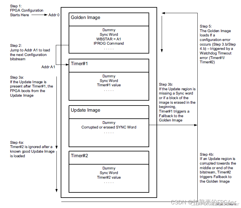
看Xilinx官方提供的fallback流程:
3.1 Step 3b:
"If the Update region is missing a Sync word or if a block of the image is erased in the begging. Timer#1 triggers a Fallback to the Golden image."
结合Xilinx配置手册中提供的KU040 BitsTREAM的举例说明:
16个word的dummy pad word 0xFFFF_FFFF + 1个word的bus width auto detect 0x0000_00BB + 1个word的bus width auto detect 0x1122_0044 + 1个word的sync word 0xAA99_5566
可以看到Sync word在第16+1+1+1= 19字的地址处,加载到此处的时间可以计算:
这里以X4 SPI举例
19 * 32 bits / 4/ 36.4MHz = 4.16us << 450us
这里可以确认的是,要加载到Sync word处,官方脚本提供的Timer1能够满足条件,且Timer1的值的确还挺小。
那整个程序(Update)的加载时间呢?以35MB举例,当然这是上限,正常到不了这么高:
35MB * 8 * 1024 * 1024 /4 /36.4MHz = 2s >> 450us
综上,Timer1的值的确远小于整个程序的加载时间,但是又能满足Sync word的找寻时间
3.2 Step 4b:
"If the Update region is corrupted towards the middle or end of the bitstream, Timer#2 triggers Fallback to the Golden Image."
对于Timer2的使用,从看门狗的值来看,这里就是敷衍过去了。。。
从配置手册上未能找到更进一步的定义,这一块,bitstream的middle或者end处,到底是怎么定义的,实际是不清楚的
4 看门狗值分析
从目前的分析来看,Xilinx的双看门狗,Timer1起到了fallback的绝大部分功能,要解决这个疑问,也许还得进一步请教原厂的研发人员了。。。
另外为何Xilinx官方提供的看门狗生成工具,为何Timer1和Timer2的值不发生变化,不论是改变SPI位宽,还是改变加载频率,均无法发生变化;这里盲猜几点:
(1)Sync Word的位置固定,无需动态调整Timer1,而Timer本身无用;
(2)bug
(3)支持用户手动计算/调整