过程(Procedures)
- Always块 -- 组合逻辑 (Always blocks -- Combinational)
由于数字电路是由电线相连的逻辑门组成的,所以任何电路都可以表示为模块和赋值语句的某种组合.
然而,有时这不是描述电路最方便的方法.
两种always block是十分有用的:
- 组合逻辑:
always @(*) - 时序逻辑:
always @(posedge clk)
always @(*)就相当于赋值语句--assign,因此选择哪一种语法仅仅取决与方便程度.
block内还有更丰富的语句集,比如if-else,case等等.但不能包含连续赋值 ,即不可包含assign,因为他与always @(*)冲突.
以下语句是等价的
verilog
assign out1 = a & b | c ^ d;
always @(*) out2 = a & b | c ^ d;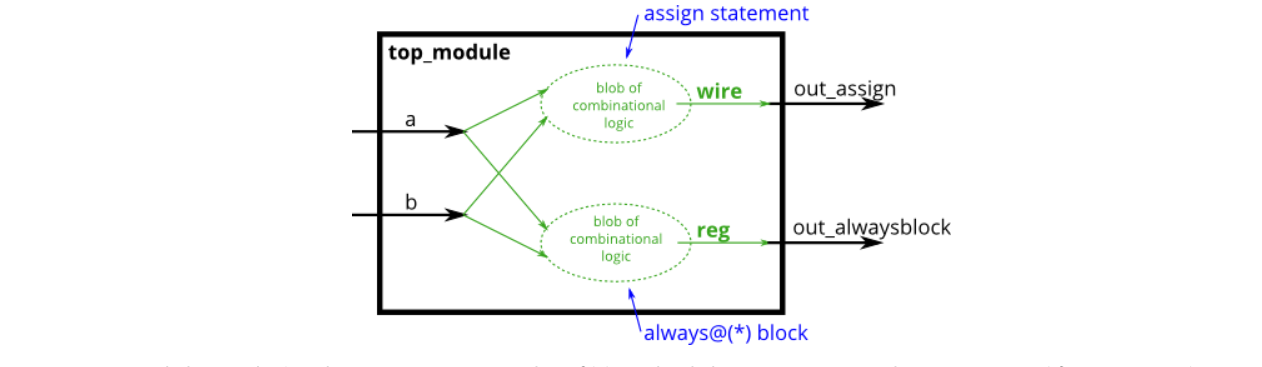
- Module Declaraction
verilog
module top_module(
    input a,
    input b,
    output wire out_assign,
    output reg out_alwaysblock
);- Solution
verilog
// synthesis verilog_input_version verilog_2001
module top_module(
    input a,
    input b,
    output wire out_assign,
    output reg out_alwaysblock
);
	assign out_assign = a&b;

    always @(*) out_alwaysblock = a&b;
endmodule
- Always块 -- 时序逻辑 (Always blocks -- Clocked)
verilog中有三种赋值方式:
- 连续赋值:
assign x = y;不能在always-block内使用 - 阻塞赋值:
x = y;, 只能在always-block内使用 - 非阻塞赋值:
x <= y,只能在always-block内使用
请在组合逻辑中使用阻塞赋值,在时序逻辑中使用非阻塞赋值
否则将产生难以发现的错误
请实现如下电路:
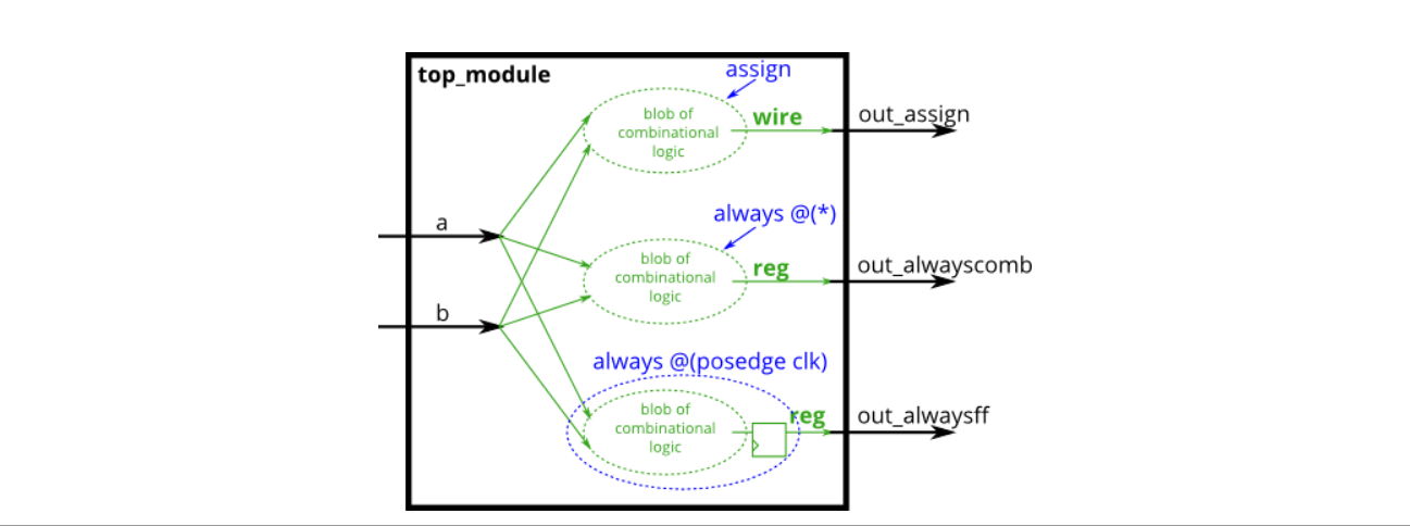
- Module Declaraction
verilog
module top_module(
    input clk,
    input a,
    input b,
    output wire out_assign,
    output reg out_always_comb,
output reg out_always_ff );- Solution
verilog
// synthesis verilog_input_version verilog_2001
module top_module(
    input clk,
    input a,
    input b,
    output wire out_assign,
    output reg out_always_comb,
    output reg out_always_ff   );
assign out_assign = a^b;

    always @(*) out_always_comb = a^b;

    always @(posedge clk) out_always_ff <= a^b;
endmodule
- If语句
if语句通常创建一个2对1的多路选择器,如果条件为真,则选择一个输入,如果条件为假,则选择另一个输入.
以下两种写法是等价的:
verilog
always @(*) begin
    if (condition) begin
        out = x;
    end
    else begin
        out = y;
    end
end

assign out = (condition) ? x : y;
建立一个在a和b之间选择的2对1多路选择器.如果sel_b1和sel_b2都为真,则选择b.否则,选择a.
执行相同的操作两次,一次使用assign语句,一次使用if语句.
- Module Declaraction
verilog
module top_module(
    input a,
    input b,
    input sel_b1,
    input sel_b2,
    output wire out_assign,
output reg out_always ); - Solution
verilog
// synthesis verilog_input_version verilog_2001
module top_module(
    input a,
    input b,
    input sel_b1,
    input sel_b2,
    output wire out_assign,
    output reg out_always   );
    assign out_assign = (sel_b1&sel_b2)?b:a;

    always @(*) begin
        if(sel_b1&sel_b2) begin
            out_always = b;
        end
        else begin
            out_always = a;
        end
    end
endmodule
- If语句引发的锁存(latches)
以下代码包含锁存的错误行为.
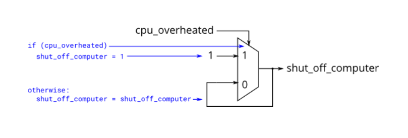
- Module Declaraction
verilog
always @(*) begin
    if (cpu_overheated)
       shut_off_computer = 1;
end

always @(*) begin
    if (~arrived)
       keep_driving = ~gas_tank_empty;
end- Solution
verilog
// synthesis verilog_input_version verilog_2001
module top_module (
    input      cpu_overheated,
    output reg shut_off_computer,
    input      arrived,
    input      gas_tank_empty,
    output reg keep_driving  ); //

    always @(*) begin
        if (cpu_overheated) begin
            shut_off_computer = 1;
        end
        else begin
            shut_off_computer = 0;
        end
    end

    always @(*) begin
        if (~arrived&~gas_tank_empty) begin
            keep_driving = ~gas_tank_empty&(~arrived);
       end
       else begin
           keep_driving = ~(gas_tank_empty|arrived);
       end
    end

endmodule
If语句在硬件描述语言(如Verilog)中用于描述受条件控制的电路。然而,不当的If语句使用可能会引发锁存器(latches)的产生,这在FPGA或ASIC设计中通常是不希望看到的。以下是对If语句引发锁存器的详细分析:
- 一、锁存器的基本概念
锁存器是一种在异步电路系统中对输入信号电平敏感的单元,用来存储信息。当锁存信号有效时,数据被锁存,输入信号不再起作用。锁存器也被称为透明锁存器,因为不锁存时输出对于输入是透明的。
-
二、If语句引发锁存器的情况
在Verilog中,If语句引发锁存器的情况主要包括以下几种:
-
组合逻辑中If语句缺少Else分支:
- 在组合逻辑电路中,如果If语句没有覆盖所有可能的条件,并且没有提供Else分支来指定其他条件下的输出,那么综合工具可能会推断出一个锁存器行为来保持上一个状态。
- 例如,
if (enable) reg <= data;当enable为假时,reg的值将保持不变,这可能导致锁存器的产生。
-
敏感信号列表不完整:
- 在
always块中使用非阻塞赋值(<=)时,如果没有显式的敏感信号列表或者敏感信号列表不完整,也可能导致锁存器的产生。 - 这是因为综合器可能无法正确判断何时应更新信号,从而推断出锁存器行为来保持信号状态。
- 在
-
输出变量赋值给自己:
- 在If语句或组合逻辑中,如果输出变量被赋值给自己(即赋值表达式中包含输出变量自身),也可能导致锁存器的产生。
- 这是因为输出变量需要具有存储功能来保持其上一个状态。
-
-
三、避免If语句引发锁存器的策略
为了避免If语句引发锁存器,可以采取以下策略:
-
确保If语句结构完整:
- 在组合逻辑中,确保If语句覆盖所有可能的条件,并提供Else分支来指定其他条件下的输出。
- 这有助于确保输出在所有条件下都有一个已知的状态,从而避免锁存器的产生。
-
使用阻塞赋值明确表达组合逻辑:
- 在组合逻辑中,使用阻塞赋值(
=)来明确表达逻辑关系,而不是使用非阻塞赋值。 - 这有助于综合工具正确识别组合逻辑并避免推断出锁存器。
- 在组合逻辑中,使用阻塞赋值(
-
完善敏感信号列表:
- 在使用非阻塞赋值时,确保
always块有完整的敏感信号列表。 - 这有助于综合工具正确判断何时应更新信号并避免锁存器的产生。
- 在使用非阻塞赋值时,确保
-
避免输出变量赋值给自己:
- 在组合逻辑中,避免将输出变量赋值给自己。
- 如果需要保持上一个状态,可以考虑使用触发器(Flip-Flop)而不是锁存器。
-
-
四、锁存器的危害与替代方案
锁存器在FPGA或ASIC设计中可能带来以下危害:
- 不可预测的时序行为:锁存器的输出取决于输入信号的持续电平,而不是特定的时钟边沿,这使得时序分析和预测更加困难。
- 系统不稳定:由于锁存器的输出直接由输入决定,任何输入上的噪声或毛刺都会立即反映到输出上,可能导致系统不稳定或误操作。
- 资源利用率降低:FPGA内部的锁存器实现通常不如寄存器高效,可能降低资源利用率并增加功耗。
因此,在FPGA设计中,通常推荐使用寄存器(触发器)来代替锁存器,除非有特殊的应用场景要求锁存器的使用。寄存器在时钟边沿更新,提供了更可预测和稳定的行为,便于时序分析和设计验证。
综上所述,If语句在硬件描述语言中的使用需要谨慎,以避免引发不必要的锁存器。通过确保If语句结构完整、使用阻塞赋值明确表达组合逻辑、完善敏感信号列表以及避免输出变量赋值给自己等策略,可以有效避免锁存器的产生。
- Case语句
verilog中的case语句几乎等同于if elseif else的序列,该序列将一个表达式与其他表达式列表进行比较.它的语法和功能与C语言中的switch语句不同.
verilog
always @(*) begin     // This is a combinational circuit
    case (in)
      1'b1: begin
               out = 1'b1;  // begin-end if >1 statement
            end
      1'b0: out = 1'b0;
      default: out = 1'bx;
    endcase
end- case语句以case开头,每个"case item"以冒号结尾,没有switch
- 每个case项只能执行一条语句.这使得C中使用的"break"不必要.但这意味着如果需要多个语句,必须使用begin...end
如果有大量选项的情况,case语句比if语句更方便.因此,在本练习中,创建一个6对1的多路选择器.当sel介于0和5之间时,选择相应的数据输入,否则,输出0.数据输入和输出均为4位宽.小心锁存.
- Module Declaraction
verilog
module top_module (
    input [2:0] sel,
    input [3:0] data0,
    input [3:0] data1,
    input [3:0] data2,
    input [3:0] data3,
    input [3:0] data4,
    input [3:0] data5,
output reg [3:0] out );- Solution
verilog
// synthesis verilog_input_version verilog_2001
module top_module (
    input [2:0] sel,
    input [3:0] data0,
    input [3:0] data1,
    input [3:0] data2,
    input [3:0] data3,
    input [3:0] data4,
    input [3:0] data5,
    output reg [3:0] out   );//

    always@(*) begin  // This is a combinational circuit
        case(sel)
            3'b0: begin
                out = data0;
            end
            3'b001: begin
                out = data1;
            end
            3'b010: begin
                out = data2;
            end
            3'b011: begin
                out = data3;
            end
            3'b100: begin
                out = data4;
            end
            3'b101: begin
                out = data5;
            end
            default: begin
                out[3:0] = 0;
            end
        endcase
    end

endmodule
- 简单编码器1
priority encoder是一种组合电路,当输入一个vector时,输出第一个'1'出现的位置.例如:输入8'b10010000,输出3'd4,因为4是第一个高位.
构建一个4位encoder,若全是低位则输出0.
- Module Declaraction
verilog
module top_module (
    input [3:0] in,
output reg [1:0] pos );- Solution
verilog
// synthesis verilog_input_version verilog_2001
module top_module (
    input [3:0] in,
    output reg [1:0] pos  );
    always @(*) begin
        if (in[0] == 1'b1) begin
                pos = 2'd0;
        end
        else begin
            if(in[1] == 1'b1) begin
                pos = 2'd1;
            end
            else begin
                if(in[2] == 1'b1) begin
                    pos = 2'd2;
                end
                else begin
                    if(in[3] == 1'b1) begin
                        pos = 2'd3;
                    end
                    else begin
                        pos = 0;
                    end
                end
            end
        end
    end
endmodule
- 简单编码器2
假如现在输入是8位,那么就会有256种情况,我们可以使用casez来将item减少到9种.
例如:
verilog
always @(*) begin
    casez (in[3:0])
        4'bzzz1: out = 0;   // in[3:1] can be anything
        4'bzz1z: out = 1;
        4'bz1zz: out = 2;
        4'b1zzz: out = 3;
        default: out = 0;
    endcase
end- Module Declaraction
verilog
module top_module (
    input [7:0] in,
output reg [2:0] pos );- Solution
verilog
// synthesis verilog_input_version verilog_2001
module top_module (
    input [7:0] in,
    output reg [2:0] pos  );
always @(*) begin
    casez (in[7:0])
        8'bzzzzzzz1: begin
            pos = 3'd0;
        end
        8'bzzzzzz1z: begin
            pos = 3'd1;
        end
        8'bzzzzz1zz: begin
            pos = 3'd2;
        end
        8'bzzzz1zzz: begin
            pos = 3'd3;
        end
        8'bzzz1zzzz: begin
            pos = 3'd4;
        end
        8'bzz1zzzzz: begin
            pos = 3'd5;
        end
        8'bz1zzzzzz: begin
            pos = 3'd6;
        end
        8'b1zzzzzzz: begin
            pos = 3'd7;
        end
        default: begin
            pos = 0;
        end
    endcase
end
endmodule
- 避免锁存
假设您正在构建一个电路来处理游戏中PS/2键盘的扫描代码.
接收到的最后两个字节的扫描代码,您需要判断是否已按下键盘上的一个箭头键.这涉及到一个相当简单的映射,它可以使用一个case语句(或者如果elseif)实现,有四个case.
| Scancode 15:0 | Arrow key |
|---|---|
| 16'he06b | left arrow |
| 16'he072 | down arrow |
| 16'he074 | right arrow |
| 16'he075 | up arrow |
| Anything | else none |
为了避免创建锁存,必须在所有可能的条件下为所有输出分配一个值
- Module Declaraction
verilog
module top_module (
    input [15:0] scancode,
    output reg left,
    output reg down,
    output reg right,
output reg up ); - Solution
verilog
// synthesis verilog_input_version verilog_2001
module top_module (
    input [15:0] scancode,
    output reg left,
    output reg down,
    output reg right,
    output reg up  );
    always @(*) begin
        left = 0;
        down = 0;
        left = 0;
        right = 0;
        case (scancode)
            16'he06b: begin
                left = 1;
            end
            16'he072: begin
                down = 1;
            end
            16'he074: begin
                right = 1;
            end
            16'he075: begin
                up = 1;
            end
            default: begin
                up = 0;
                down = 0;
                left = 0;
                right = 0;
            end
        endcase
    end
endmodule
更多语法特点
verilog也有像C一样的三目算符:
- 三目算符
verilog也有像C一样的三目算符:
verilog
condition ? true : false;给定四个无符号数,求其最小值.
- Module Declaraction
verilog
module top_module (
    input [7:0] a, b, c, d,
output [7:0] min);- Solution
verilog
module top_module (
    input [7:0] a, b, c, d,
    output [7:0] min);//

    // assign intermediate_result1 = compare? true: false;

    wire [7:0]min1,min2;
    assign min1=(a<b?a:b);

    assign min2 = (min1<c?min1:c);

    assign min = (min2<d?min2:d);
endmodule
- 优化运算1
奇偶校验经常被用来作为一种简单的方法检测错误.
创建一个电路,该电路将为一个8位字节计算一个奇偶校验位.
即计算输入8个位的异或
- Module Declaraction
verilog
module top_module (
    input [7:0] in,
output parity); - Solution
verilog
module top_module (
    input [7:0] in,
    output parity);
    assign parity = ^in[7:0];
endmodule
- 优化运算2
建立如下电路:
-
out_and: 对输入数据求与 -
out_or: 对输入数据求或 -
out_xor:对输入数据求异或 -
Module Declaraction
verilog
module top_module(
    input [99:0] in,
    output out_and,
    output out_or,
    output out_xor
);- Solution
verilog
module top_module(
    input [99:0] in,
    output out_and,
    output out_or,
    output out_xor
);
    assign out_and = &in[99:0];
    assign out_or = |in[99:0];
    assign out_xor = ^in[99:0];
endmodule
- 循环 -- 组合逻辑:实现Vector反转
反转vector顺序
- Module Declaraction
verilog
module top_module(
    input [99:0] in,
    output [99:0] out
);- Solution
verilog
module top_module(
    input [99:0] in,
    output [99:0] out
);
    integer i;
    always @(*) begin
        for(i=0;i<=99;i=i+1)
            out[7'd99-i] <= in[i];
    end
endmodule
- 循环 -- 组合逻辑:实现255位计数器
计算vector中1的个数
- Module Declaraction
verilog
module top_module(
    input [254:0] in,
output [7:0] out );- Solution
verilog
module top_module(
    input [254:0] in,
    output [7:0] out );
    integer i;
    reg [7:0]count;
    always @(*) begin

	count=0;
        for(i=0;i<=254;i=i+1) begin
            if(in[i] == 1) begin
                count = count + 7'b1;
            end
        end
    end
    assign out = count;
endmodule
- 循环:实现100位加法器
通过实例化100个全加器构建一个100位加法器.
- Module Declaraction
verilog
module top_module(
    input [99:0] a, b,
    input cin,
    output [99:0] cout,
output [99:0] sum );- Solution
verilog
module top_module(
    input [99:0] a, b,
    input cin,
    output [99:0] cout,
    output [99:0] sum );
    reg [100:0]cin1;

    generate
    genvar i;
    for(i=0;i<100;i=i+1) begin:adds

        if(i==0) begin
		    add ins(a[i],b[i],cin,sum[i],cout[i]);
            assign cin1[i+1]=cout[i];
        end
        else begin
            add ins(a[i],b[i],cin1[i],sum[i],cout[i]);
            assign cin1[i+1]=cout[i];
        end
    end
    endgenerate
endmodule

module add(input a, input b, input cin, output sum, output cout);
    assign {cout,sum}=a+b+cin;
endmodule
- 循环:实现100位BCD加法器
在Verilog中实现一个100位的BCD(Binary-Coded Decimal)加法器相对复杂,因为BCD编码的每个数字占用4位二进制数,所以100位的BCD数实际上表示的是25位的十进制数(100位 / 4位/十进制数字 = 25个十进制数字)。
BCD加法的一个关键问题是进位处理。在普通的二进制加法中,进位是逐位传递的,但在BCD加法中,每四位(一个BCD数字)之间可能需要额外的调整来处理从低位到高位的进位,以确保结果仍然是有效的BCD数。这通常涉及到将非BCD的中间结果转换为BCD格式。
以下是一个简化的Verilog代码示例,用于实现两个4位BCD数的加法,并调整结果以确保它是有效的BCD数。请注意,这个示例并没有直接扩展到100位,但它提供了一个基础,你可以在这个基础上构建更复杂的100位BCD加法器。
verilog
module bcd_adder_4bit(
    input [3:0] a, // 4-bit BCD input
    input [3:0] b, // 4-bit BCD input
    input cin,     // Carry-in
    output [3:0] sum, // 4-bit BCD output
    output cout    // Carry-out
);
    wire [4:0] temp_sum; // 5-bit temporary sum to handle carry
    wire [3:0] adjusted_sum; // 4-bit adjusted BCD sum
    wire temp_cout; // Temporary carry-out

    // Perform binary addition of the BCD digits and the carry-in
    assign temp_sum = a + b + cin;
    assign temp_cout = (temp_sum[4] == 1'b1); // Carry-out if the sum is 5-bits wide

    // BCD adjustment: if the result is greater than or equal to 10 (0xA in BCD), adjust it
    // to be in the range 0-9 by subtracting 6 (0x6 in BCD) and setting the carry-out for the next BCD digit
    assign adjusted_sum = (temp_sum >= 4'd10) ? (temp_sum - 4'd6) : temp_sum[3:0];

    // Carry-out for the next BCD digit is set if the original sum was 10 or more, or if there was a carry-in and the sum was exactly 9
    wire carry_adjustment = (temp_sum == 4'd10) | (cin && temp_sum == 4'd9);
    assign cout = temp_cout | carry_adjustment;

    // Output the adjusted sum
    assign sum = adjusted_sum;

endmodule要构建一个100位的BCD加法器,你需要将上述4位BCD加法器模块级联25次(因为100位/4位/数字=25个数字)。每个模块的输出cout将作为下一个模块的cin。同时,你需要一个额外的机制来处理最高位可能产生的进位(如果两个加数的和超过最大的25位BCD数)。
请注意,这个示例代码没有考虑所有可能的边界情况和优化。在实际应用中,你可能需要更复杂的逻辑来处理溢出、零检测、符号扩展等问题。此外,对于大规模设计,使用高级综合工具或手动优化可能有助于提高性能和资源利用率。