还记得之前软件的同事说过的一句话。怎么凸显自己的工作量,就是自己给自己写BUG。
看过夏宇闻老师书的都知道,verilog的FSM有moore和mealy,然后有一段,二段,三段式。记得我还是学生的时候,看到这里的时候,感觉很烧脑。毕竟这与数字电路设计息息相关。
今天我想把问题简单化。只谈mealy型三段式写法。
借用前辈们总结的一句话说:三段式描述方法虽然代码结构复杂了一些,但是换来的优势是使 FSM 做到了同步寄存器输出,消除了组合逻辑输出的不稳定与毛刺的隐患,而且更利于时序路径分组,一般来说在 FPGA/CPLD 等可编程逻辑器件上的综合与布局布线效果更佳。
(闪耀着哲学的光辉......)
bash
//3-paragraph method to describe FSM
//Describe sequential state transition in the 1st sequential always block
//State transition conditions in the 2nd combinational always block
//Describe the FSM out in the 3rd sequential always block
//Verilog Training -- How to write FSM better
module state3 ( rst_n,
clk,
i1,
i2,
o1,
o2,
err
);
input rst_n,clk;
input i1,i2;
output o1,o2,err;
reg o1,o2,err;
reg [2:0] NS,CS;
//one hot with zero idle
parameter [2:0] IDLE = 3'b000;
parameter [2:0] S1 = 3'b001;
parameter [2:0] S2 = 3'b010;
parameter [2:0] ERROR = 3'b100;
//1st always block, sequential state transition
always @(posedge clk or negedge rst_n)
if (!rst_n)
CS <= IDLE;
else
CS <=NS;
//2nd always block, combinational condition judgment
always @ (rst_n or CS or i1 or i2)
begin
NS = 3'bx;
case (CS)
IDLE: begin
if (~i1) NS = IDLE;
if (i1 && i2) NS = S1;
if (i1 && ~i2) NS = ERROR;
end
S1: begin
if (~i2) NS = S1;
if (i2 && i1) NS = S2;
if (i2 && (~i1)) NS = ERROR;
end
S2: begin
if (i2) NS = S2;
if (~i2 && i1) NS = IDLE;
if (~i2 && (~i1)) NS = ERROR;
end
ERROR: begin
if (i1) NS = ERROR;
if (~i1) NS = IDLE;
end
endcase
end
//3rd always block, the sequential FSM output
always @ (posedge clk or negedge rst_n)
if (!rst_n)
{o1,o2,err} <= 3'b000;
else
begin
{o1,o2,err} <= 3'b000;
case (NS)
IDLE: {o1,o2,err}<=3'b000;
S1: {o1,o2,err}<=3'b100;
S2: {o1,o2,err}<=3'b010;
ERROR: {o1,o2,err}<=3'b111;
endcase
end
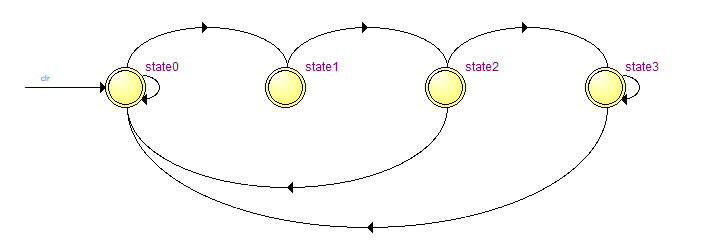
endmodule同样这段代码也很好理解:
bash
module FSM(
			clk,
			clr,
			out,
			start,
			step2,
			step3
		);
input				clk;
input				clr;
input				start;
input				step2;
input				step3;

output[2:0]			out;

reg[2:0]			out;
reg[1:0]			state,next_state;


/*状态编码,采用格雷(Gray)编码方式*/
parameter						state0 = 2'b00;
parameter						state1 = 2'b01;
parameter						state2 = 2'b11;
parameter						state3 = 2'b10;

/*该进程定义起始状态*/
always @(posedge clk or posedge clr)
begin
	if (clr)
		state <= state0;
	else
		state <= next_state;
end

/*该进程实现状态的转换*/
always @(state or start or step2 or step3)
begin
	case (state)
		state0: begin
			if (start)
				next_state <=state1;
			else
				next_state <=state0;
		end

		state1: begin
			next_state <= state2;
		end

		state2: begin
			if (step2)
				next_state <=state3;
			else
				next_state <=state0;
		end

		state3: begin
			if (step3)
				next_state <=state0;
			else
				next_state <=state3;
		end

		default: next_state <=state0; /*default语句*/
	endcase
end

/*该进程定义组合逻辑(FSM的输出)*/
always @(state)
begin
	case(state)

		state0: out=3'b001;
		state1: out=3'b010;
		state2: out=3'b100;
		state3: out=3'b111;
		default:out=3'b001;
		/*default语句,避免锁存器的产生*/

	endcase
end

endmodule
状态转移图如下:
总结
文章难免会有些水平不足,不正确的地方请大家多多指正,共同进步。