例如:
用多个
ila_1 axi_rx (
	.clk(srio_log_clk), // input wire clk

	.probe0({m_axis_treq_tvalid,m_axis_treq_tlast,m_axis_treq_tready}),// input wire [2:0]  probe0
	.probe1(m_axis_treq_tdata), // input wire [63:0]  probe1
	.probe2(m_axis_treq_tuser), // input wire [31:0]  probe2
	.probe3(m_axis_treq_tkeep) // input wire [7:0]  probe3
);

用一个大位宽
ila_1 axi_rx (
	.clk(srio_log_clk), // input wire clk

	.probe0({m_axis_treq_tvalid,m_axis_treq_tlast,m_axis_treq_tready,m_axis_treq_tdata,m_axis_treq_tuser,m_axis_treq_tkeep})// input wire [2:0]  probe0
多个probe资源使用情况
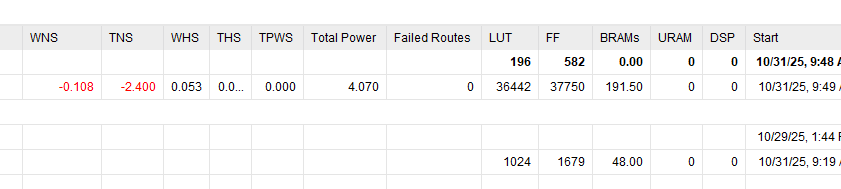
一个大位宽资源使用情况:
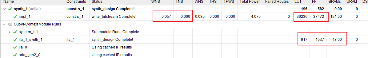
注意:发现时序也变好了