文章目录
前言
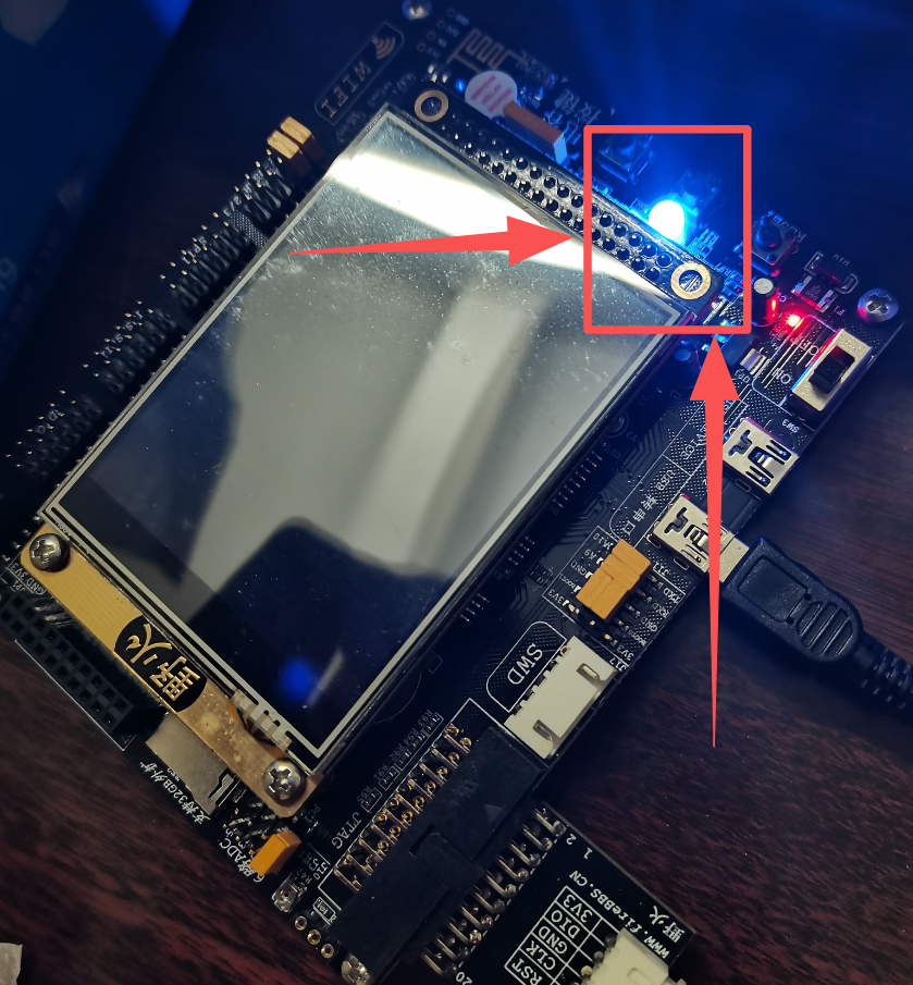
开发板为:野火指南者,基于STM32F103VET6
分析的例程为:指南者\1-程序源码_教程文档\2-[野火]《STM32 HAL库开发实战指南》(HAL库源码)\12-GPIO输出---使用固件库点亮LED灯
1.GPIO
通过HAL库操作GPIOB的关键函数或数据结构如下:
c
// 1、使能GPIO时钟
__HAL_RCC_GPIOB_CLK_ENABLE()
 // 2、配置GPIO工作模式
void HAL_GPIO_Init(GPIO_TypeDef* GPIOx, GPIO_InitTypeDef* GPIO_Init)
 // 3、控制GPIOB输出状态
void HAL_GPIO_WritePin(GPIO_TypeDef *GPIOx, uint16_t GPIO_Pin, GPIO_PinState PinState)
接下来逐行分析上述的3行代码
1.1.使能GPIOB时钟
✅__HAL_RCC_GPIOB_CLK_ENABLE()在STM32F1xx_HAL_Driver\Inc\stm32f1xx_hal_rcc.h文件中的511行,如下面代码所示
c
// 🚀1、
#define __HAL_RCC_GPIOB_CLK_ENABLE()   do { \
                                        __IO uint32_t tmpreg; \
                                        SET_BIT(RCC->APB2ENR, RCC_APB2ENR_IOPBEN);\
                                        /* Delay after an RCC peripheral clock enabling */\
                                        tmpreg = READ_BIT(RCC->APB2ENR, RCC_APB2ENR_IOPBEN);\
                                        UNUSED(tmpreg); \
                                      } while(0U)
c
// 🚀2、展开👇
#define __HAL_RCC_GPIOB_CLK_ENABLE()  do { \
                                        __IO uint32_t tmpreg; \
                                        (RCC->APB2ENR) |= (RCC_APB2ENR_IOPBEN);\
                                        /* Delay after an RCC peripheral clock enabling */\
                                        tmpreg = (RCC->APB2ENR) & (RCC_APB2ENR_IOPBEN);\
                                        (void)tmpreg;\
                                      } while(0U)

// 🚀3、删掉不重要的代码得到👇
#define __HAL_RCC_GPIOB_CLK_ENABLE()  (RCC->APB2ENR) |= (RCC_APB2ENR_IOPBEN);
c
// 🚀4、关于RCC以及RCC_APB2ENR_IOPBEN的定义👇
typedef struct
{
  __IO uint32_t CR;			// 偏移0字节
  __IO uint32_t CFGR;			// 偏移4字节
  __IO uint32_t CIR;			// 偏移8字节
  __IO uint32_t APB2RSTR;	// 偏移12字节
  __IO uint32_t APB1RSTR;	// 偏移16字节
  __IO uint32_t AHBENR;		// 偏移20字节
  __IO uint32_t APB2ENR;	// 偏移24字节, 即偏移0x18字节
  __IO uint32_t APB1ENR;
  __IO uint32_t BDCR;
  __IO uint32_t CSR;
} RCC_TypeDef;

#define RCC  ((RCC_TypeDef *)RCC_BASE)

RCC_BASE = (AHBPERIPH_BASE + 0x00001000UL)
         = ((PERIPH_BASE + 0x00020000UL) + 0x00001000UL)
         = ((0x40000000UL+ 0x00020000UL) + 0x00001000UL)

RCC_APB2ENR_IOPBEN = (0x1UL << RCC_APB2ENR_IOPBEN_Pos) = (0x1UL << 3U) = 0000 0000 0000 1000 = 0x00000008UL
c
// 🚀5、把第🚀4部分代码合并到第🚀3部分后得到👇
RCC->APB2ENR = *(unsigned int *)(((0x40000000UL+ 0x00020000UL) + 0x00001000UL) + 0x00000018UL)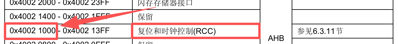
RCC->APB2ENR |= 0x00000008UL✅通过查询《STM32F10xxx参考手册》的2.3存储器映像章节得知
复位和时钟控制(RCC) 的基地址 = ((0x40000000UL+ 0x00020000UL) + 0x00001000UL)) = 0x40021000UL
✅通过查询《STM32F10xxx参考手册》的6.3.11 RCC寄存器地址映像章节得知
RCC_APB2ENR的地址 =(((0x40000000UL+ 0x00020000UL) + 0x00001000UL) + 0x00000018UL) = 0x40021018UL
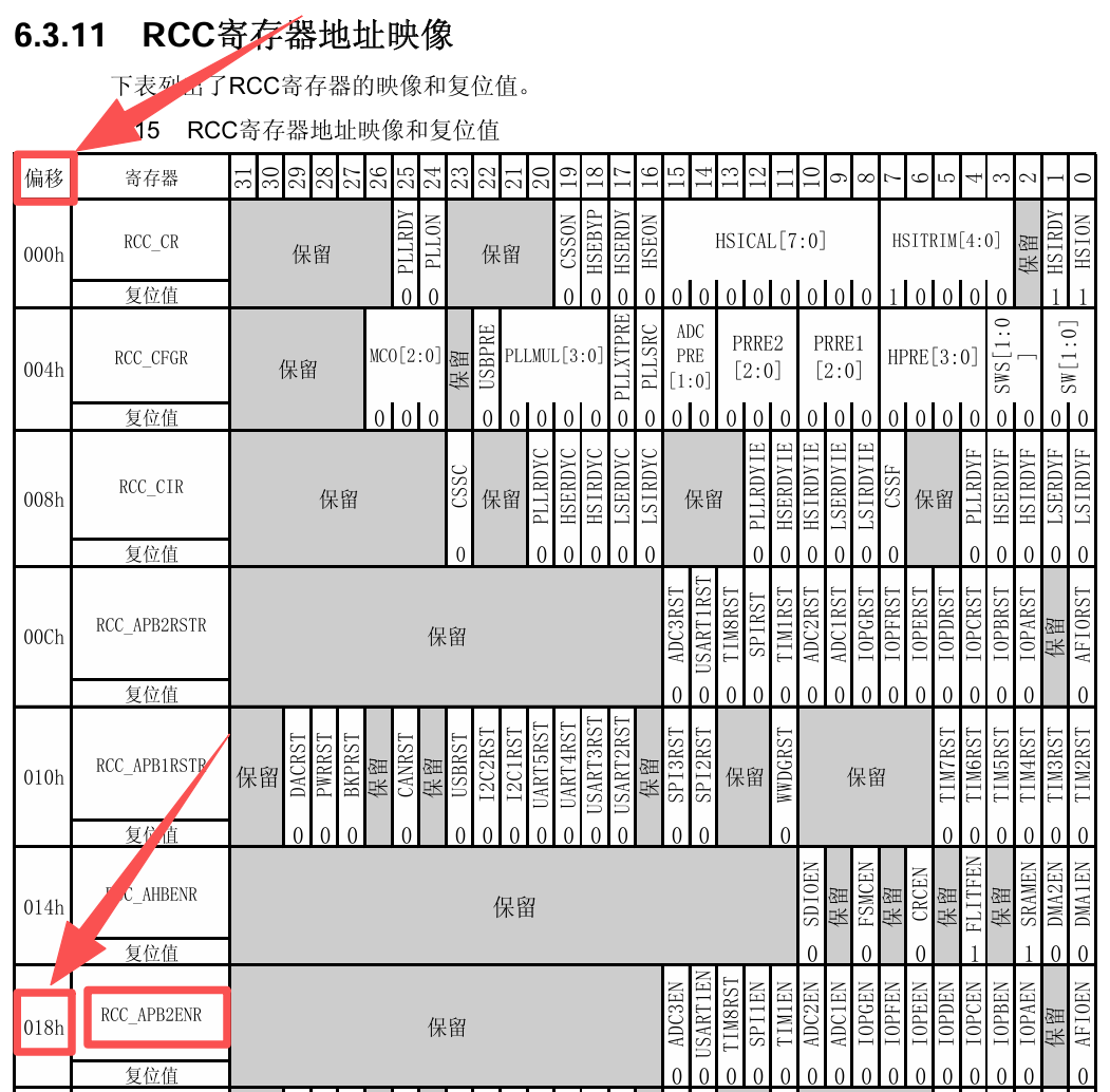
✅通过查询通过查询《STM32F10xxx参考手册》的6.3.7 APB2外设时钟使能寄存器(RCC_APB2ENR)章节得知
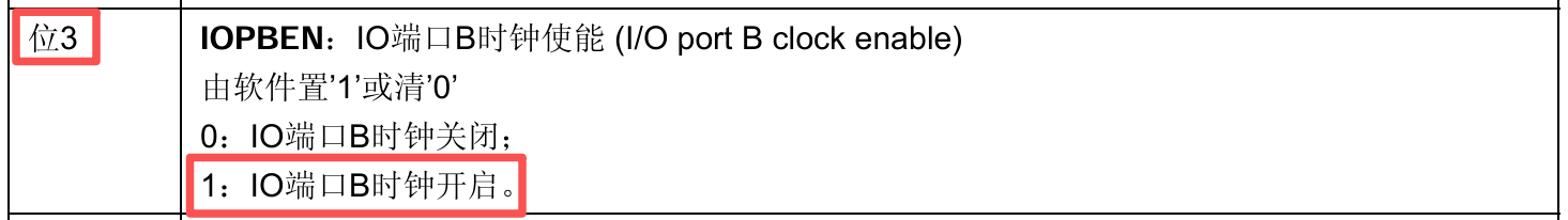
RCC_APB2ENR的bit3是用于使能GPIOB的时钟
1.2.配置GPIO工作方式
✅void HAL_GPIO_Init(GPIO_TypeDef *GPIOx, GPIO_InitTypeDef *GPIO_Init)在STM32F1xx_HAL_Driver\Src\stm32f1xx_hal_gpio.c文件中的178行,函数定义如下
c
/**
  * @brief  Initializes the GPIOx peripheral according to the specified parameters in the GPIO_Init.
  * @param  GPIOx: where x can be (A..G depending on device used) to select the GPIO peripheral
  * @param  GPIO_Init: pointer to a GPIO_InitTypeDef structure that contains
  *         the configuration information for the specified GPIO peripheral.
  * @retval None
  */
void HAL_GPIO_Init(GPIO_TypeDef  *GPIOx, GPIO_InitTypeDef *GPIO_Init)
{
  uint32_t position = 0x00u;
  uint32_t ioposition;
  uint32_t iocurrent;
  uint32_t temp;
  uint32_t config = 0x00u;
  __IO uint32_t *configregister; /* Store the address of CRL or CRH register based on pin number */
  uint32_t registeroffset;       /* offset used during computation of CNF and MODE bits placement inside CRL or CRH register */

  /* Check the parameters */
  assert_param(IS_GPIO_ALL_INSTANCE(GPIOx));
  assert_param(IS_GPIO_PIN(GPIO_Init->Pin));
  assert_param(IS_GPIO_MODE(GPIO_Init->Mode));

  /* Configure the port pins */
  while (((GPIO_Init->Pin) >> position) != 0x00u)
  {
    /* Get the IO position */
    ioposition = (0x01uL << position);

    /* Get the current IO position */
    iocurrent = (uint32_t)(GPIO_Init->Pin) & ioposition;

    if (iocurrent == ioposition)
    {
      /* Check the Alternate function parameters */
      assert_param(IS_GPIO_AF_INSTANCE(GPIOx));

      /* Based on the required mode, filling config variable with MODEy[1:0] and CNFy[3:2] corresponding bits */
      switch (GPIO_Init->Mode)
      {
        /* If we are configuring the pin in OUTPUT push-pull mode */
        case GPIO_MODE_OUTPUT_PP:
          /* Check the GPIO speed parameter */
          assert_param(IS_GPIO_SPEED(GPIO_Init->Speed));
          config = GPIO_Init->Speed + GPIO_CR_CNF_GP_OUTPUT_PP;
          break;

        /* If we are configuring the pin in OUTPUT open-drain mode */
        case GPIO_MODE_OUTPUT_OD:
          /* Check the GPIO speed parameter */
          assert_param(IS_GPIO_SPEED(GPIO_Init->Speed));
          config = GPIO_Init->Speed + GPIO_CR_CNF_GP_OUTPUT_OD;
          break;

        /* If we are configuring the pin in ALTERNATE FUNCTION push-pull mode */
        case GPIO_MODE_AF_PP:
          /* Check the GPIO speed parameter */
          assert_param(IS_GPIO_SPEED(GPIO_Init->Speed));
          config = GPIO_Init->Speed + GPIO_CR_CNF_AF_OUTPUT_PP;
          break;

        /* If we are configuring the pin in ALTERNATE FUNCTION open-drain mode */
        case GPIO_MODE_AF_OD:
          /* Check the GPIO speed parameter */
          assert_param(IS_GPIO_SPEED(GPIO_Init->Speed));
          config = GPIO_Init->Speed + GPIO_CR_CNF_AF_OUTPUT_OD;
          break;

        /* If we are configuring the pin in INPUT (also applicable to EVENT and IT mode) */
        case GPIO_MODE_INPUT:
        case GPIO_MODE_IT_RISING:
        case GPIO_MODE_IT_FALLING:
        case GPIO_MODE_IT_RISING_FALLING:
        case GPIO_MODE_EVT_RISING:
        case GPIO_MODE_EVT_FALLING:
        case GPIO_MODE_EVT_RISING_FALLING:
          /* Check the GPIO pull parameter */
          assert_param(IS_GPIO_PULL(GPIO_Init->Pull));
          if (GPIO_Init->Pull == GPIO_NOPULL)
          {
            config = GPIO_CR_MODE_INPUT + GPIO_CR_CNF_INPUT_FLOATING;
          }
          else if (GPIO_Init->Pull == GPIO_PULLUP)
          {
            config = GPIO_CR_MODE_INPUT + GPIO_CR_CNF_INPUT_PU_PD;

            /* Set the corresponding ODR bit */
            GPIOx->BSRR = ioposition;
          }
          else /* GPIO_PULLDOWN */
          {
            config = GPIO_CR_MODE_INPUT + GPIO_CR_CNF_INPUT_PU_PD;

            /* Reset the corresponding ODR bit */
            GPIOx->BRR = ioposition;
          }
          break;

        /* If we are configuring the pin in INPUT analog mode */
        case GPIO_MODE_ANALOG:
          config = GPIO_CR_MODE_INPUT + GPIO_CR_CNF_ANALOG;
          break;

        /* Parameters are checked with assert_param */
        default:
          break;
      }

      /* Check if the current bit belongs to first half or last half of the pin count number
       in order to address CRH or CRL register*/
      configregister = (iocurrent < GPIO_PIN_8) ? &GPIOx->CRL     : &GPIOx->CRH;
      registeroffset = (iocurrent < GPIO_PIN_8) ? (position << 2u) : ((position - 8u) << 2u);

      /* Apply the new configuration of the pin to the register */
      MODIFY_REG((*configregister), ((GPIO_CRL_MODE0 | GPIO_CRL_CNF0) << registeroffset), (config << registeroffset));

      /*--------------------- EXTI Mode Configuration ------------------------*/
      /* Configure the External Interrupt or event for the current IO */
      if ((GPIO_Init->Mode & EXTI_MODE) == EXTI_MODE)
      {
        /* Enable AFIO Clock */
        __HAL_RCC_AFIO_CLK_ENABLE();
        temp = AFIO->EXTICR[position >> 2u];
        CLEAR_BIT(temp, (0x0Fu) << (4u * (position & 0x03u)));
        SET_BIT(temp, (GPIO_GET_INDEX(GPIOx)) << (4u * (position & 0x03u)));
        AFIO->EXTICR[position >> 2u] = temp;


        /* Configure the interrupt mask */
        if ((GPIO_Init->Mode & GPIO_MODE_IT) == GPIO_MODE_IT)
        {
          SET_BIT(EXTI->IMR, iocurrent);
        }
        else
        {
          CLEAR_BIT(EXTI->IMR, iocurrent);
        }

        /* Configure the event mask */
        if ((GPIO_Init->Mode & GPIO_MODE_EVT) == GPIO_MODE_EVT)
        {
          SET_BIT(EXTI->EMR, iocurrent);
        }
        else
        {
          CLEAR_BIT(EXTI->EMR, iocurrent);
        }

        /* Enable or disable the rising trigger */
        if ((GPIO_Init->Mode & RISING_EDGE) == RISING_EDGE)
        {
          SET_BIT(EXTI->RTSR, iocurrent);
        }
        else
        {
          CLEAR_BIT(EXTI->RTSR, iocurrent);
        }

        /* Enable or disable the falling trigger */
        if ((GPIO_Init->Mode & FALLING_EDGE) == FALLING_EDGE)
        {
          SET_BIT(EXTI->FTSR, iocurrent);
        }
        else
        {
          CLEAR_BIT(EXTI->FTSR, iocurrent);
        }
      }
    }

	position++;
  }
}
✅假设我们执行的代码如下
c
#define GPIOB  (GPIO_TypeDef *) GPIOB_BASE

GPIO_InitTypeDef  GPIO_InitStruct;
GPIO_InitStruct.Pin = GPIO_PIN_5;
GPIO_InitStruct.Mode  = GPIO_MODE_OUTPUT_PP;
GPIO_InitStruct.Pull  = GPIO_PULLUP;
GPIO_InitStruct.Speed = GPIO_SPEED_FREQ_HIGH;

HAL_GPIO_Init(GPIOB, &GPIO_InitStruct); ✅由于GPIO_InitStruct没有配置外部中断,那么我们可以把void HAL_GPIO_Init(GPIO_TypeDef *GPIOx, GPIO_InitTypeDef *GPIO_Init)中外部中断的配置代码、断言代码、switch中非GPIO_MODE_OUTPUT_PP模式的代码删掉,便于分析代码,于是得到👇
c
// 🚀1、简化后的HAL_GPIO_Init函数定义👇
void HAL_GPIO_Init(GPIO_TypeDef  *GPIOx, GPIO_InitTypeDef *GPIO_Init)
{
  uint32_t position = 0x00u;
  uint32_t ioposition;
  uint32_t iocurrent;
  uint32_t temp;
  uint32_t config = 0x00u;
  __IO uint32_t *configregister;
  uint32_t registeroffset;
  // 遍历并配置GPIO_Init->Pin的每一个引脚,从STM32F1xx_HAL_Driver\Inc\stm32f1xx_hal_gpio.h文件的第83行可以知道
  // GPIOB有16个引脚宏,每个引脚对应一个bit位,GPIO_Init->Pi = GPIO_PIN_5 = 0x0010 = 0000 0000 0001 0000对应了bit5
  while (((GPIO_Init->Pin) >> position) != 0x00u)
  {
    // ioposition在while循环中从0000 0000 000 0001 -> 1000 0000 000 010 -> ... -> 1000 0000 000 000
    ioposition = (0x01uL << position);
    // ioposition作为掩码和GPIO_Init->Pin进行按位与运算,找到需要配置的IO口
    iocurrent = (uint32_t)(GPIO_Init->Pin) & ioposition;
    // 当iocurrent == ioposition的时候,成功找到一个需要配置的IO口
    if (iocurrent == ioposition)
    {
      // 根据GPIO_Init->Mode对IO口进行工作方式的配置
      switch (GPIO_Init->Mode)
      {
        // 配置成开漏输出
        case GPIO_MODE_OUTPUT_PP:
          config = GPIO_Init->Speed + GPIO_CR_CNF_GP_OUTPUT_PP;
          break;
      }
      /* Check if the current bit belongs to first half or last half of the pin count number
       in order to address CRH or CRL register*/
      configregister = (iocurrent < GPIO_PIN_8) ? &GPIOx->CRL     : &GPIOx->CRH;
      registeroffset = (iocurrent < GPIO_PIN_8) ? (position << 2u) : ((position - 8u) << 2u);
      /* Apply the new configuration of the pin to the register */
      MODIFY_REG((*configregister), ((GPIO_CRL_MODE0 | GPIO_CRL_CNF0) << registeroffset), (config << registeroffset));
   }
   position++;
}
c
// 🚀2、从🚀1中我们可以看出,配置寄存器的就这4行代码
config = GPIO_Init->Speed + GPIO_CR_CNF_GP_OUTPUT_PP;
configregister = (iocurrent < GPIO_PIN_8) ? &GPIOx->CRL : &GPIOx->CRH;
registeroffset = (iocurrent < GPIO_PIN_8) ? (position << 2u) : ((position - 8u) << 2u);
MODIFY_REG((*configregister), ((GPIO_CRL_MODE0 | GPIO_CRL_CNF0) << registeroffset), (config << registeroffset));
c
// 🚀3、我们继续
// 所以现在的分析思路要转换一下,我们要找到作者到底要操作哪个寄存器,然后查《STM32F10xxx参考手册》,所以先展开MODIFY_REG
#define READ_REG(REG)  ((REG))
#define MODIFY_REG(REG, CLEARMASK, SETMASK)  WRITE_REG((REG), (((READ_REG(REG)) & (~(CLEARMASK))) | (SETMASK)))
// MODIFY_REG(REG, CLEARMASK, SETMASK)👉相当于👉REG = (REG & (~CLEARMASK)) | (SETMASK)

// 🚀4、所以作者要操作的寄存器是REG = (*configregister) = &GPIOx->CRL = (iocurrent < GPIO_PIN_8) ? &GPIOx->CRL : &GPIOx->CRH
// GPIOx = GPIOB,GPIOB的定义如下
typedef struct
{
  __IO uint32_t CRL;
  __IO uint32_t CRH;
  __IO uint32_t IDR;
  __IO uint32_t ODR;
  __IO uint32_t BSRR;
  __IO uint32_t BRR;
  __IO uint32_t LCKR;
} GPIO_TypeDef;
#define PERIPH_BASE           0x40000000UL
#define APB2PERIPH_BASE       (PERIPH_BASE + 0x00010000UL)
#define GPIOB_BASE            (APB2PERIPH_BASE + 0x00000C00UL)
#define GPIOB  ((GPIO_TypeDef *)GPIOB_BASE)
// 所以作者要操作的寄存器是
configregister = &GPIOx->CRL = (0x40000000UL + 0x00010000UL) + 0x00000C00UL = 0x40010C00UL
c
// 🚀5、把MODIFY_REG宏展开后得到
// MODIFY_REG(REG, CLEARMASK, SETMASK)👉相当于👉REG = (REG & (~CLEARMASK)) | (SETMASK)

// REG = (*(&GPIOx->CRL)) = (*0x40010C00UL)

// ~CLEARMASK = ((GPIO_CRL_MODE0 | GPIO_CRL_CNF0) << registeroffset)
//            = ((0x3UL | (0x3UL << 2U)) << 20)
//            = ~((0011  | (1100)) << 20)
//            = 1111 1111 0000 1111 1111 1111 1111 1111b

// SETMASK = (config << registeroffset)
//         = (0x3UL << 20)
//         = 1111 1111 0011 1111 1111 1111 1111 1111b

// 即把GPIOB pin5 设置为 推挽输出模式,最大速度50MHZ
(*0x40010C00UL) = ((*0x40010C00UL) & (1111 1111 0000 1111 1111 1111 1111 1111b)) | 1111 1111 0011 1111 1111 1111 1111 1111b✅通过查询《STM32F10xxx参考手册》的2.3存储器映像章节得知
GPIO端口B的基地址 = ((0x40000000UL + 0x00010000UL)+ 0x00000C00UL) = 0x40010C00UL
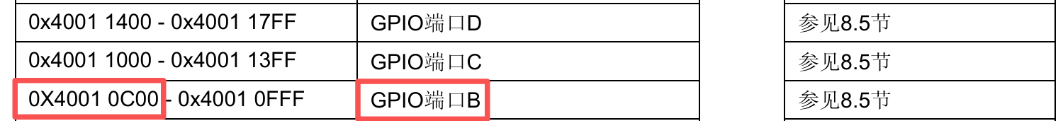
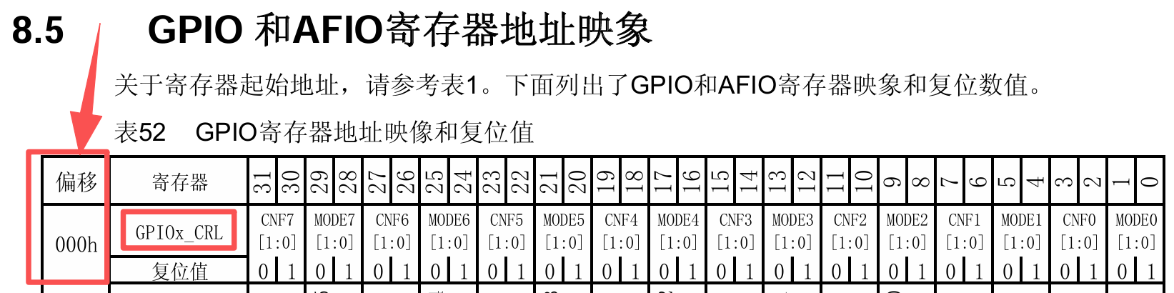
✅通过查询《STM32F10xxx参考手册》的8.5 GPIO和AFIO寄存器地址映象章节得知
GPIO端口B的基地址 = ((0x40000000UL + 0x00010000UL)+ 0x00000C00UL) = 0x40010C00UL在0偏移时,对应寄存器GPIOx_CRL,
 ✅通过查询《STM32F10xxx参考手册》的
8.2.1 端口配置低寄存器(GPIOx_CRL)章节得知
寄存器GPIOx_CRL,负责配置GPIOx的第0-7个引脚,对应手册中y = 0-7,每个引脚占用4位的寄存器。
从这里可以推断出为什么registeroffset需要左移2位 ,因为position代表着当前while循环中配置第几个引脚,position << 2相当于position * 4,正好复合手册中每个引脚需要占用GPIOx_CRL的4bit的描述,而由于一共有16个引脚,所以一个32bit的寄存器只能管理8个引脚,从这里可以推断出为什么((position - 8u) << 2u)
c
registeroffset = (iocurrent < GPIO_PIN_8) ? (position << 2u) : ((position - 8u) << 2u);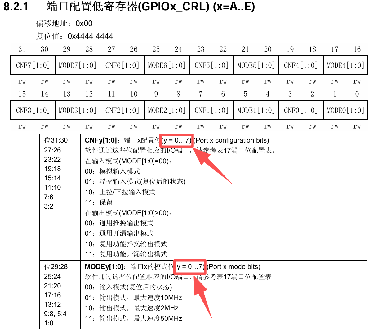
✅在推导出结果后,我们知道void HAL_GPIO_Init(GPIO_TypeDef *GPIOx, GPIO_InitTypeDef *GPIO_Init)函数就是用来配置GPIOx_CRL或GPIOx_CRH寄存器的。此时我们回头重新看👇三行代码,就很清晰了
c
config = GPIO_Init->Speed + GPIO_CR_CNF_GP_OUTPUT_PP; // config = 0x3UL + 0x00000000u
configregister = (iocurrent < GPIO_PIN_8) ? &GPIOx->CRL : &GPIOx->CRH;
registeroffset = (iocurrent < GPIO_PIN_8) ? (position << 2u) : ((position - 8u) << 2u);GPIO_Init->Speed:用来配置GPIOx_CRL或GPIOx_CRH的MODEy[1:0]GPIO_CR_CNF_GP_OUTPUT_PP:用来配置GPIOx_CRL或GPIOx_CRH的CNFy[1:0]configregister:用来确认当前配置的是GPIOx_CRL还是GPIOx_CRHregisteroffset:用来确认当前配置的是GPIOx_CRL或GPIOx_CRH的哪个引脚
1.3.控制GPIOB输出状态
✅HAL_GPIO_WritePin()在STM32F1xx_HAL_Driver\Src\stm32f1xx_hal_gpio.c文件中的465行,如下面代码所示
c
// 🚀1
void HAL_GPIO_WritePin(GPIO_TypeDef *GPIOx, uint16_t GPIO_Pin, GPIO_PinState PinState)
{
  /* Check the parameters */
  assert_param(IS_GPIO_PIN(GPIO_Pin));
  assert_param(IS_GPIO_PIN_ACTION(PinState));

  if (PinState != GPIO_PIN_RESET)
  {
    GPIOx->BSRR = GPIO_Pin;
  }
  else
  {
    GPIOx->BSRR = (uint32_t)GPIO_Pin << 16u;
  }
}
c
// 🚀2、简化后得到
void HAL_GPIO_WritePin(GPIO_TypeDef *GPIOx, uint16_t GPIO_Pin, GPIO_PinState PinState)
{
  if (PinState != GPIO_PIN_RESET)
    GPIOx->BSRR = GPIO_Pin;
  else
    GPIOx->BSRR = (uint32_t)GPIO_Pin << 16u;
}
✅假设我们执行的代码如下
c
HAL_GPIO_WritePin(GPIOB, GPIO_PIN_5, GPIO_PIN_SET)✅关键代码就2行
c
// 🚀3、操作寄存器的关键代码
// 置位
GPIOx->BSRR = GPIO_Pin;
// 复位
GPIOx->BSRR = (uint32_t)GPIO_Pin << 16u;
c
// 🚀4、继续展开代码
// GPIOx = GPIOB,GPIOB的定义如下
typedef struct
{
  __IO uint32_t CRL;
  __IO uint32_t CRH;
  __IO uint32_t IDR;
  __IO uint32_t ODR;
  __IO uint32_t BSRR;
  __IO uint32_t BRR;
  __IO uint32_t LCKR;
} GPIO_TypeDef;
#define PERIPH_BASE           0x40000000UL
#define APB2PERIPH_BASE       (PERIPH_BASE + 0x00010000UL)
#define GPIOB_BASE            (APB2PERIPH_BASE + 0x00000C00UL)
#define GPIOB  ((GPIO_TypeDef *)GPIOB_BASE)
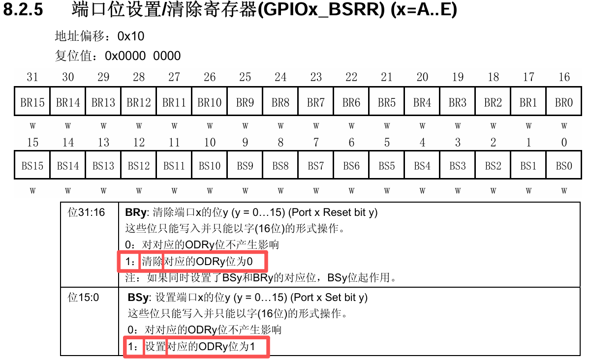
&GPIOx->BSRR = ((0x40000000UL + 0x00010000UL) + 0x00000C00UL) + 0x10;✅同样的套路,先看《STM32F10xxx参考手册》的2.3章节找基地址,接着根据地址偏移量0x10找到具体的寄存器,从手册中可以发现,要置位或清零,直接往对应的引脚位写1即可
2.不用库函数,点亮LED灯
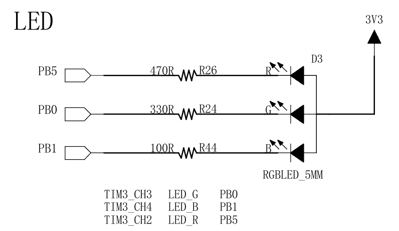
✅电路原理图如下,我们只要让GPIOB的PIN1,推挽输出模式,输出低电平,即可让LED_B蓝色亮起来
c
int main(void)
{
	SystemClock_Config();
	// 1. RCC_APB2ENR
	*(unsigned int*)0x40021018 |= 0x08UL;
	// 2. GPIOx_CRL
	*(unsigned int*)0X40010C00 = (*(unsigned int*)0X40010C00) & (~0xF0UL);
	*(unsigned int*)0X40010C00 |= 0x30UL;
	// 3. GPIOx_BSSR
	*(unsigned int*)0X40010C10 |= (0x01UL << 16);
}
3.总结
GPIO的使用,分3步走:
- 使能GPIO的时钟,寄存器:
RCC_APB2ENR - 配置GPIO的工作模式,寄存器:
GPIOx_CRL、GPIOx_CRH - 控制GPIO的输出状态,寄存器:
GPIOx_BSSR