文章目录
- 引言
- SPI总线的基本原理与拓扑结构
- 传输的四种模式(核心时序)
- [使用 FPGA 实现 SPI 控制器的 N 种方法](#使用 FPGA 实现 SPI 控制器的 N 种方法)
- [Verilog实现IIC 主从机](#Verilog实现IIC 主从机)
- [优点 & 缺点:](#优点 & 缺点:)
引言
在嵌入式系统和数字电路设计中,芯片间的通信至关重要。在众多的串行通信协议中,SPI(Serial Peripheral Interface,串行外设接口)以其全双工、同步传输、连线简单(通常只需4根线)的特点,被广泛应用于传感器、ADC、DAC、Flash存储器等外设的连接。
对于FPGA或ASIC工程师而言,仅仅会调用SPI IP核是不够的,深入理解其时序并掌握使用Verilog实现Master(主机)和Slave(从机)的设计思路,是进阶的必经之路。本文将带你图文结合地梳理SPI的核心要点。
SPI总线的基本原理与拓扑结构
SPI是一种同步、全双工的通信总线。所谓"同步",意味着通信双方共用一个时钟信号;所谓"全双工",意味着在同一时刻,数据可以同时进行发送和接收。
四根核心信号线
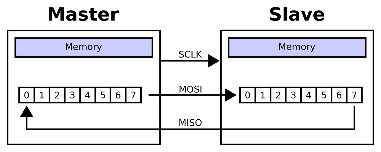
SPI通信主要依靠以下四根信号线完成:
- SCLK (Serial Clock):串行时钟,永远由主机发出,用于同步数据传输。
- MOSI (Master Out Slave In):主机输出,从机输入数据线。
- MISO (Master In Slave Out):主机输入,从机输出数据线。
- CS / SS (Chip Select / Slave Select):片选信号,通常由主机控制,低电平有效。用于选中特定的从机进行通信。
数据交换的本质
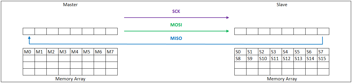
SPI通信的本质其实是"移位寄存器的数据交换"。主机和从机内部各有一个移位寄存器。在SCLK时钟的驱动下,主机寄存器里的最高位(MSB)通过MOSI线移入从机的最低位(LSB),同时从机寄存器里的最高位通过MISO线移入主机的最低位。经过8个(或更多)时钟周期后,主机和从机里的数据就完成了一次互换。
两种典型拓扑结构
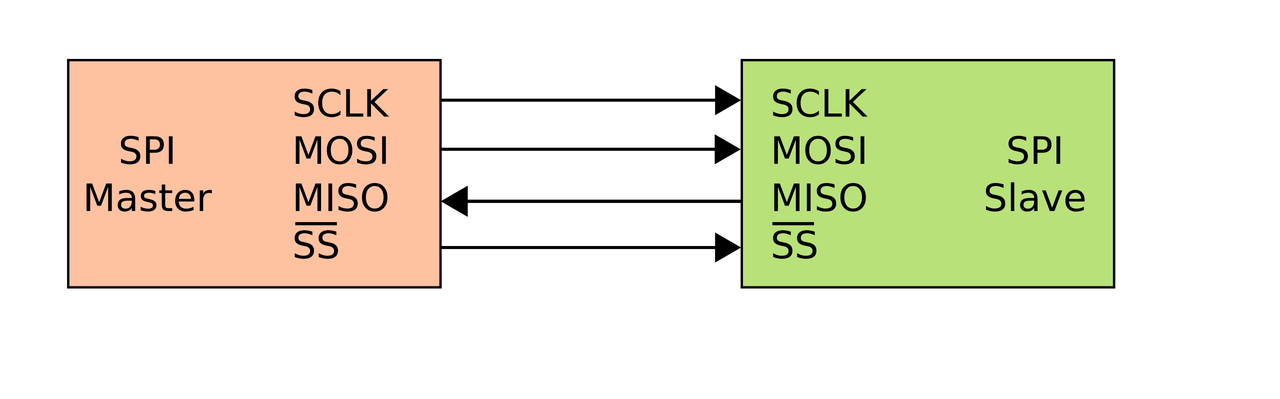
① 一主一从 (Single Master - Single Slave)
这是最简单的连接方式。主机通过一根专用的CS线连接到唯一的从机。当主机拉低CS信号时,通信开始。
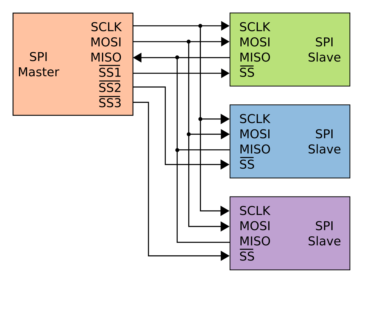
② 一主多从 (Single Master - Multiple Slaves)
在实际应用中,一个主机往往需要挂载多个从机。SPI支持这种拓扑。
- SCLK、MOSI、MISO这三根线在所有设备间是共用的(总线式)。
- 关键在于CS片选线。主机必须为每一个从机提供一根独立的CS信号线(如CS1, CS2, CS3)。
- 在某一时刻,主机只能拉低其中一个从机的CS线,此时只有被选中的从机占用MISO线与主机通信,其他未被选中的从机其MISO引脚必须处于高阻态(Hi-Z),以避免总线冲突。
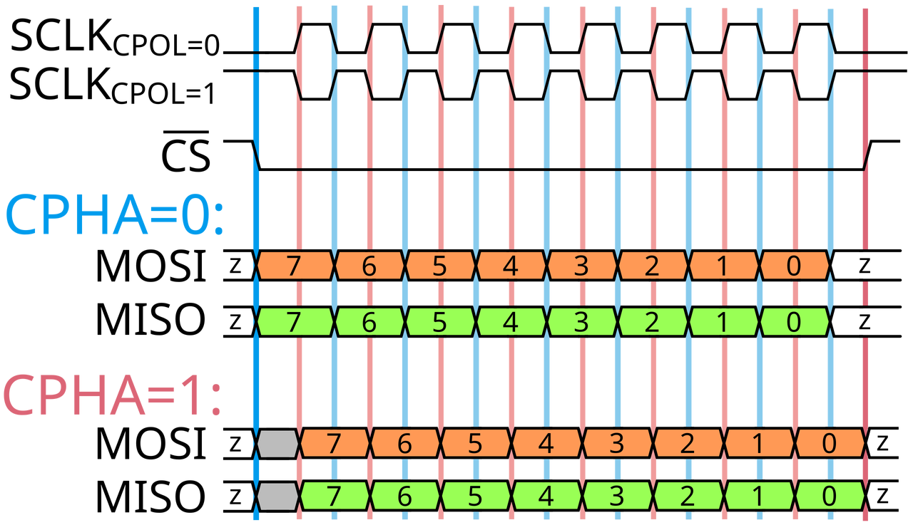
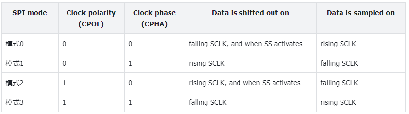
传输的四种模式(核心时序)
这是SPI最容易让人困惑的地方。不同的SPI设备可能工作在不同的模式下,如果主机和从机的模式配置不一致,通信就会失败。
SPI的四种模式由两个参数决定:CPOL (Clock Polarity, 时钟极性) 和 CPHA (Clock Phase, 时钟相位)。
- CPOL (时钟极性):决定了SCLK在空闲状态(即CS为高电平,没有数据传输时)的电平。
- CPOL = 0:SCLK空闲时为低电平。
- CPOL = 1:SCLK空闲时为高电平。
- CPHA (时钟相位):决定了数据是在SCLK的第几个边沿被采样(读取)。
- CPHA = 0:数据在SCLK的第一个跳变沿(上升沿或下降沿,取决于CPOL)被采样。数据通常在片选拉低后立刻准备好。
- CPHA = 1:数据在SCLK的第二个跳变沿被采样。数据在前一个边沿进行移位/更新。
根据CPOL和CPHA的不同组合,形成了四种标准的SPI模式。理解下图是掌握SPI时序的关键:
使用 FPGA 实现 SPI 控制器的 N 种方法
在 Xilinx FPGA 开发中,实现 SPI 通常有几种方式:
- 使用 AXI QUAD SPI IP 核:
- 适用场景: 配合 MicroBlaze 软核或 Zynq/MPSoC 的 PL 端扩展。
- 特点: 官方 IP,功能全(支持 Standard/Dual/Quad 模式),驱动完善。
- 缺点: 依赖 AXI 总线,占用较多 LUT 资源,不够轻量,且交互时序受限于 AXI 总线延迟。
- 使用 Zynq/MPSoC PS 端的 MIO SPI:
- 适用场景: 嵌入式 Linux 或裸机开发,外设直接挂在 PS 端。
- 特点: 直接走芯片内部硬核,不占用任何 PL 逻辑资源,性能稳定。
- 缺点: 受限于 MIO 引脚分配(MIO 引脚数量固定且位置不可变), PCB 布线灵活性差。
- 使用 Zynq/MPSoC PS 端的 EMIO SPI:
- 适用场景: 需要使用 PS 硬核驱动,但 MIO 引脚不够用或外设连接在 PL 端引脚时。
- 特点: 将 PS 端的硬核 SPI 信号通过 EMIO 路由到 PL 端的任意引脚。既保留了硬核驱动的便利性,又拥有了 PL 引脚分配的灵活性。
- 缺点: 相比 MIO,信号经过 PL 会引入微小的延时(通常可忽略)。
- 使用 GPIO 模拟 SPI :
- 适用场景: 对速度要求极低(如几 KHz)的配置接口,或者临时调试。
- 特点: 使用 AXI GPIO (PL) 或 PS GPIO 通过软件拉高拉低引脚来模拟时序。
- 缺点: 效率极低,严重占用 CPU 资源,无法实现高速传输,容易被中断打断导致时序错误。
- 纯 RTL 手写实现(本文重点):
- 适用场景: 高速 ADC/DAC 采集、FPGA 逻辑直接控制外设、非标准位宽/协议、由于资源限制无法使用软核时。
- 特点: 灵活性最高。不依赖 CPU 和 AXI 总线,时序完全可控,延迟最低,资源占用最小。
- 去处理器化: 很多时候 FPGA 是作为协处理器存在的,它需要自主从 SPI 接口的传感器(如加速度计、陀螺仪、ADC)读取数据并处理,然后再打包发给 CPU。如果每次读取都要 CPU 介入,系统的实时性会大打折扣。
- 非标协议: 很多工业或军工芯片名为 "SPI",实则在时序上有很多魔改(比如需要 24bit 传输,或者 CS 信号有特殊拉高要求),标准 IP 核往往无法满足,只能手写。
Verilog实现IIC 主从机
SPI主机
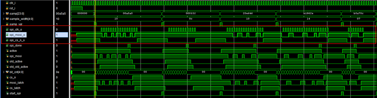
以模式0,SPI主机写功能为例,展示两种SPI主机驱动代码,这两种代码的区别主要在于时钟生成机制和适用频率。 如果是高速 SPI(如 >25MHz),为了保证时钟质量和时序对齐,我会用 ODDR 原语来驱动; 如果是低速 SPI(如 <1MHz),对时序要求不高,我会直接用逻辑计数器分频生成时钟,这样代码通用性更好。
【设计文件】spi_driver.v
c
//-----------------------------------------------------------------------------
//
//  Copyright (c) 2009 Xilinx Inc.
//
//  Project  : Programmable Wave Generator
//  Module   : dac_spi.v
//  Parent   : wave_gen
//  Children : None
//
//  Description:
//     This module takes each sample generated by the sample generator and
//     sends it to the digital to analog converter (DAC) using the SPI
//     protocol. Each SPI cycle is 32 clocks long, consisting of an address,
//     command, and 16 bits of data (MSbit first). The DAC on the development
//     boards use only the most significant 12 out of the 16 bit samples, but
//     all 16 bits are transmitted.
//
//  Parameters:
//
//  Local Parameters:
//
//  Notes       :
//
//  Multicycle and False Paths
//    None.
//
//

module spi_driver (
     input                               clk_i                      // Clock input
    ,input                               rst_i                      // Active HIGH reset - synchronous to clk_i
    ,input                [  23: 0]      samp                       // Sample output
    ,input                [   4: 0]      sample_width
    ,input                               samp_val                   // New sample is available

    ,output                              spi_clk_o                  // Clock for SPI - generated by DDR flop
    ,output reg                          spi_mosi_o                 // SPI master-out-slave-in data bit
    ,output reg                          spi_cs_n_o                 // Chip select for DAC
    ,output reg                          spi_done                   // SPI transaction is complete
);

//***************************************************************************
// Parameter definitions
//***************************************************************************

//***************************************************************************
// Reg and Wire declarations
//***************************************************************************

    reg                                 active                      ; // Indicates that this module is sending a seq
    reg                                 old_active                  ; // The value of active on the last clock
    reg                                 old_old_active              ; // The value of active on the previous clock
    reg                [   4: 0]        bit_cnt                     ; // Counts from 30 to 0
    reg                                 spi_mosi                    ; // SPI master-out-slave-in data bit
    reg                                 cs_n                        ; // Chip select

    reg                                 mosi_latch                  ;
    reg                                 cs_latch                    ;

//***************************************************************************
// Code
//***************************************************************************

    // We start a new sequence when samp_val is asserted, and this is the
    // "active" phase (i.e. the last one) of clk_samp
    assign start_spi = samp_val;

    // Generate the SPI protocol
    always @(posedge clk_i) begin
        if (rst_i) begin
            active         <= 1'b0;
            old_active     <= 1'b0;
            old_old_active <= 1'b0;
            bit_cnt        <= 5'b00000;
            cs_n           <= 1'b1;      // Active low
            spi_mosi       <= 1'b1;      // Idle at 1'b1
        end else begin
            old_active     <= active;
            old_old_active <= old_active;
            if (!active) begin
                if (start_spi) begin
                    active       <= 1'b1;                   // Go active
                    cs_n         <= 1'b0;                   // Set CS active
                    spi_mosi     <= samp[sample_width-1];   // Send the first bit of the seq
                    bit_cnt      <= sample_width-2'd2;      // We have already sent sample_width-1
                end else begin
                    cs_n         <= 1'b1;                   // INACTIVE
                    spi_mosi     <= 1'b1;
                end
            end else begin // we are currently active
                spi_mosi   <= samp[bit_cnt];
                if (bit_cnt == 5'b00000) begin // This is the last bit
                    active  <= 1'b0;
                end else begin // Not the last bit
                    bit_cnt <= bit_cnt - 1'b1;
                end
            end
        end // if rst
    end // always

    always @(posedge clk_i) begin
        if (rst_i) begin
            spi_done <= 1'b0;
        end else begin
            if (bit_cnt == 5'b00001) begin
                spi_done <= 1'b1;
            end else begin
                spi_done <= 1'b0;
            end
        end
    end

    // Pipeline the outputs
    always @(posedge clk_i) begin
        mosi_latch   <= spi_mosi;
        cs_latch     <= cs_n;
    end

    always @(posedge clk_i) begin
        spi_mosi_o   <= mosi_latch;
        spi_cs_n_o   <= cs_latch;
    end

    // Generate the SPI clock using the DDR flop
    // It is based on old_active due to the pipelining of the other
    // signals, and it is extended one extra clock to allow for the clocking
    // of the last bit (old_old_active).
    out_ddr_flop I_OUT_DDR_FLOP_SPI_CLK (
         .clk                                ( clk_i                     )
        ,.rst                                ( 1'b0                      )
        ,.d_rise                             ( 1'b0                      )
        ,.d_fall                             ( old_active || old_old_active)
        ,.q                                  ( spi_clk_o                 )
    );

endmodule

//-----------------------------------------------------------------------------
//
//  Copyright (c) 2009 Xilinx Inc.
//
//  Project  : Programmable Wave Generator
//  Module   : out_ddr_flop.v
//  Parent   : Various
//  Children : None
//
//  Description:
//    This is a wrapper around a basic DDR output flop.
//    A version of this module with identical ports exists for all target
//    technologies for this design (Spartan 3E and Virtex 5).
//
//
//  Parameters:
//    None
//
//  Notes       :
//
//  Multicycle and False Paths, Timing Exceptions
//     None
//

`timescale 1ns/1ps

module out_ddr_flop (
  input            clk,          // Destination clock
  input            rst,          // Reset - synchronous to destination clock
  input            d_rise,       // Data for the rising edge of clock
  input            d_fall,       // Data for the falling edge of clock
  output           q             // Double data rate output
);

//***************************************************************************
// Register declarations
//***************************************************************************

//***************************************************************************
// Code
//***************************************************************************

   // ODDR: Output Double Data Rate Output Register with Set, Reset
   //       and Clock Enable.
   //       Virtex-4/5
   // Xilinx HDL Language Template, version 11.1

   ODDRE1 #(
      .IS_C_INVERTED(1'b0),  // Optional inversion for C
      .IS_D1_INVERTED(1'b0), // Optional inversion for D1
      .IS_D2_INVERTED(1'b0), // Optional inversion for D2
      .SRVAL(1'b0)           // Initializes the ODDRE1 Flip-Flops to the specified value (1'b0, 1'b1)
   )
   ODDRE1_inst (
      .Q(q),   // 1-bit output: Data output to IOB
      .C(clk),   // 1-bit input: High-speed clock input
      .D1(d_rise), // 1-bit input: Parallel data input 1
      .D2(d_fall), // 1-bit input: Parallel data input 2
      .SR(rst)  // 1-bit input: Active High Async Reset
   );

   // End of ODDR_inst instantiation

endmodule
仿真时序:
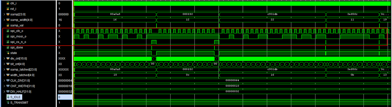
【设计文件】spi_driver_low.v
c
`timescale 1ns / 1ps

module spi_driver_low #(
    // 参数配置
    // 系统时钟频率 / SPI目标频率 = 分频系数
    // 例如: 100MHz / 1MHz = 100
    parameter CLK_DIV = 100
)(
    input  wire        clk_i,
    input  wire        rst_i,
    input  wire [23:0] samp,
    input  wire [ 4:0] samp_width,
    input  wire        samp_val,

    output reg         spi_clk_o,
    output reg         spi_mosi_o,
    output reg         spi_cs_n_o,
    output reg         spi_done
);

    //-------------------------------------------------------------------------
    // 常量定义 (状态机与计算)
    //-------------------------------------------------------------------------
    // 自动计算计数器位宽
    // function integer clog2; ... endfunction 在Verilog 2001中通常用常数或手动计算
    // 这里为了兼容性,假设分频系数不会超过 8位 (255),如果很大请增加位宽
    localparam CNT_WIDTH = 16;
    localparam DIV_HALF  = CLK_DIV / 2;

    // 状态定义 (One-Hot 或 Binary 均可,这里使用简单的 Binary)
    localparam S_IDLE     = 1'b0;
    localparam S_TRANSMIT = 1'b1;

    //-------------------------------------------------------------------------
    // 寄存器定义
    //-------------------------------------------------------------------------
    reg                 state;
    reg [CNT_WIDTH-1:0] div_cnt;      // 分频计数器
    reg [4:0]           bit_cnt;      // 位计数器

    // 输入信号锁存器 (Shadow Registers)
    reg [23:0]          samp_latched;
    reg [4:0]           width_latched;

    //-------------------------------------------------------------------------
    // 主要逻辑
    //-------------------------------------------------------------------------
    always @(posedge clk_i) begin
        if (rst_i) begin
            state         <= S_IDLE;
            spi_cs_n_o    <= 1'b1;
            spi_mosi_o    <= 1'b1;
            spi_clk_o     <= 1'b0;    // CPOL=0 (空闲时低电平)
            spi_done      <= 1'b0;
            div_cnt       <= {CNT_WIDTH{1'b0}};
            bit_cnt       <= 5'd0;
            samp_latched  <= 24'd0;
            width_latched <= 5'd0;
        end else begin
            // 默认信号行为
            spi_done <= 1'b0;

            case (state)
                //==============================================================
                // 空闲状态:等待 samp_val 信号
                //==============================================================
                S_IDLE: begin
                    spi_cs_n_o <= 1'b1;
                    spi_clk_o  <= 1'b0;
                    spi_mosi_o <= 1'b1;
                    div_cnt    <= 0;

                    if (samp_val) begin
                        // 1. 锁存输入数据 (防止传输过程中外部数据变化)
                        samp_latched  <= samp;
                        width_latched <= samp_width;

                        // 2. 立即拉低 CS (Chip Select)
                        spi_cs_n_o    <= 1'b0;

                        // 3. 准备发送最高位 (MSB)
                        // 注意:这里我们假设 sample_width 至少为1
                        bit_cnt       <= samp_width;

                        // 4. 状态跳转
                        state         <= S_TRANSMIT;
                    end
                end

                //==============================================================
                // 传输状态:生成时钟并移出数据
                //==============================================================
                S_TRANSMIT: begin
                    //--- 分频计数器逻辑 ---
                    // 不管是不是最后一位,都要让计数器走完整个周期
                    if (div_cnt == CLK_DIV - 1) begin
                        div_cnt <= 0;

                        // 此时距离上一次上升沿已经过了半个 SPI 周期,满足 CS Hold Time
                        if (bit_cnt == 0) begin
                            state      <= S_IDLE;
                            spi_done   <= 1'b1;
                            // 下一个周期进 IDLE,CS 才会拉高
                        end
                    end else begin
                        div_cnt <= div_cnt + 1'b1;
                    end

                    //--- SPI 时钟与数据移位逻辑 ---

                    // 1. 周期开始 (Falling Edge): 更新 MOSI 数据
                    if (div_cnt == 0) begin
                        spi_clk_o  <= 1'b0;
                        if (bit_cnt > 0)
                             spi_mosi_o <= samp_latched[bit_cnt - 1'b1];
                    end

                    // 2. 周期中间 (Rising Edge): 采样沿,时钟拉高
                    else if (div_cnt == DIV_HALF) begin
                        spi_clk_o <= 1'b1;

                        if (bit_cnt > 0) begin
                            bit_cnt <= bit_cnt - 1'b1;
                        end
                        // 此时 bit_cnt 变成了 0,但我们继续等到 div_cnt == CLK_DIV - 1
                    end
                end
            endcase
        end
    end

endmodule
仿真时序:
【仿真文件】tb_spi_driver.sv
c
`timescale 1ns / 1ps

module tb_spi_driver;

    //--------------------------------------------------------------------------
    // Signals Declaration
    //--------------------------------------------------------------------------
    logic          clk_i;
    logic          rst_i;
    logic [23:0]   samp;
    logic [ 4:0]   sample_width;
    logic          samp_val;

    logic          spi_clk_o;
    logic          spi_mosi_o;
    logic          spi_cs_n_o;
    logic          spi_done;

    // Clock definition (100MHz)
    parameter CLK_PERIOD = 10;

    //--------------------------------------------------------------------------
    // DUT Instantiation
    //--------------------------------------------------------------------------
    spi_driver dut (
        .clk_i        (clk_i),
        .rst_i        (rst_i),
        .samp         (samp),
        .sample_width (sample_width),
        .samp_val     (samp_val),
        .spi_clk_o    (spi_clk_o),
        .spi_mosi_o   (spi_mosi_o),
        .spi_cs_n_o   (spi_cs_n_o),
        .spi_done     (spi_done)
    );

    //--------------------------------------------------------------------------
    // Clock Generation
    //--------------------------------------------------------------------------
    initial begin
        clk_i = 0;
        forever #(CLK_PERIOD/2) clk_i = ~clk_i;
    end

    //--------------------------------------------------------------------------
    // Test Procedure
    //--------------------------------------------------------------------------
    initial begin
        // 1. Initialize Signals
        rst_i        = 1;
        samp         = 0;
        sample_width = 16;
        samp_val     = 0;

        // 2. Reset Sequence
        #(CLK_PERIOD * 5);
        rst_i = 0;
        #(CLK_PERIOD * 5);

        $display("\n--- Simulation Start ---\n");

        // 3. Test Case 1: Standard 16-bit transmission
        $display("[TEST 1] Sending 0xA5A5 with width 16");
        send_sample(24'h00A5A5, 5'd16);

        // Wait for a bit of idle time
        #(CLK_PERIOD * 10);

        // 4. Test Case 2: 12-bit transmission (Common for DACs)
        $display("[TEST 2] Sending 0xFFF with width 12");
        send_sample(24'h000FFF, 5'd12);

        #(CLK_PERIOD * 10);

        // 5. Test Case 3: Random Data and Random Width
        repeat (5) begin
            logic [23:0] rand_data;
            logic [4:0]  rand_width;

            rand_data = $urandom();
            // Constrain width between 4 and 24 to be safe/realistic
            rand_width = $urandom_range(4, 24);

            $display("[TEST RAND] Sending 0x%h with width %0d", rand_data, rand_width);
            send_sample(rand_data, rand_width);
            #(CLK_PERIOD * 5);
        end

        #(CLK_PERIOD * 20);
        $display("\n--- Simulation Passed ---\n");
        $finish;
    end

    //--------------------------------------------------------------------------
    // Driver Task
    //--------------------------------------------------------------------------
    task send_sample(input logic [23:0] data_in, input logic [4:0] width_in);
        // Synchronize to falling edge to drive inputs safely
        @(negedge clk_i);
        samp         = data_in;
        sample_width = width_in;
        samp_val     = 1'b1;

        @(negedge clk_i);
        samp_val     = 1'b0;

        // Wait for the transaction to complete
        // Note: spi_done signals logical completion, but pipeline delays
        // mean physical output might take 1-2 more clocks.
        // We wait for CS_N to go high to ensure physical completion.
        wait(spi_cs_n_o == 1'b0); // Wait for start
        wait(spi_cs_n_o == 1'b1); // Wait for end
    endtask

    //--------------------------------------------------------------------------
    // Monitor / Scoreboard (SPI Protocol Checker)
    //--------------------------------------------------------------------------
    logic [23:0] captured_data;
    int          bit_index;

    initial begin
        forever begin
            // Wait for Chip Select to go Active (Low)
            @(negedge spi_cs_n_o);

            captured_data = 0;
            bit_index = 0;

            // Capture Loop
            // While CS is low, we shift in bits.
            // Based on the DUT logic and DDR flop:
            // The DUT updates MOSI on posedge clk_i.
            // SPI_CLK is generated via DDR: Low on rise, High on fall (if active).
            // This creates a clock roughly inverted to clk_i.
            // We sample on the rising edge of SPI_CLK (middle of bit stable time).
            while (spi_cs_n_o == 1'b0) begin
                @(posedge spi_clk_o or posedge spi_cs_n_o);
                if (spi_cs_n_o == 1'b1) break; // Exit if CS went high asynchronously

                // Shift in the bit (MSB first protocol)
                captured_data = {captured_data[22:0], spi_mosi_o};
                bit_index++;
            end

            // Verify
            // Note: captured_data contains the bits shifted in.
            // We need to mask the input 'samp' to the width we tested to compare correctly.
            verify_data(captured_data, samp, sample_width);
        end
    end

    function void verify_data(logic [23:0] rx_data, logic [23:0] tx_data, logic [4:0] width);
        logic [23:0] expected_masked;

        // Create a mask for the expected data based on width
        // Example: width 4 -> mask 0x00000F
        // The DUT sends samp[width-1] down to samp[0].

        // Our captured data is right-aligned because we shifted left.
        // So rx_data should match tx_data[width-1 : 0].

        logic [23:0] tx_masked;

        // Mask the upper bits of tx_data that weren't sent
        if (width == 24)
            tx_masked = tx_data;
        else
            tx_masked = tx_data & ((1 << width) - 1);

        if (rx_data !== tx_masked) begin
            $error("[SCB] Mismatch! Width: %0d", width);
            $error("      Sent (masked): 0x%h", tx_masked);
            $error("      Recv         : 0x%h", rx_data);
        end else begin
            $display("[SCB] Match! Recv: 0x%h (Width: %0d)", rx_data, width);
        end
    endfunction

endmodule
SPI从机
【设计文件】spi_slave.v
c
module spi_slave #(
parameter DATA_WIDTH = 8,
parameter CPOL = 0, // 0: Idle Low, 1: Idle High
parameter CPHA = 0 // 0: Sample 1st edge, 1: Sample 2nd edge
)(
// 系统接口
input wire i_clk, // 系统时钟
input wire i_rst_n, // 同步复位,低电平有效
// SPI 物理接口
input wire i_spi_sclk,
input wire i_spi_cs_n,
input wire i_spi_mosi,
output wire o_spi_miso, // 顺手加上 o_ 前缀保持风格统一
// 用户接口
input wire [DATA_WIDTH-1:0] i_tx_data, // 预备发送的数据
output reg [DATA_WIDTH-1:0] o_rx_data, // 接收到的数据
output reg o_rx_done, // 接收完成脉冲
output reg o_tx_done // 发送完成脉冲
);
// ============================================================
// 1. 跨时钟域同步 (CDC)
// ============================================================
reg [2:0] sclk_sync;
reg [2:0] cs_n_sync;
reg [1:0] mosi_sync;
// 修改点:同步复位
always @(posedge i_clk) begin
if (!i_rst_n) begin
// 复位值根据 CPOL 设定,防止复位瞬间产生误判
sclk_sync <= (CPOL) ? 3'b111 : 3'b000;
cs_n_sync <= 3'b111;
mosi_sync <= 2'b00;
end else begin
sclk_sync <= {sclk_sync[1:0], i_spi_sclk};
cs_n_sync <= {cs_n_sync[1:0], i_spi_cs_n};
mosi_sync <= {mosi_sync[0], i_spi_mosi};
end
end
// 内部净信号
wire sclk_clean = sclk_sync[1];
wire cs_n_clean = cs_n_sync[1];
wire mosi_clean = mosi_sync[1];
// CS_N 下降沿检测 (用于 CPHA=0 数据预加载)
wire cs_n_negedge = (cs_n_sync[2] == 1'b1 && cs_n_sync[1] == 1'b0);
// ============================================================
// 2. 边沿检测逻辑 (支持 CPOL)
// ============================================================
wire sclk_rise = (sclk_sync[2:1] == 2'b01);
wire sclk_fall = (sclk_sync[2:1] == 2'b10);
// 前沿与后沿定义
wire leading_edge = (CPOL == 0) ? sclk_rise : sclk_fall;
wire trailing_edge = (CPOL == 0) ? sclk_fall : sclk_rise;
// 采样与移位使能
wire sample_en = (CPHA == 0) ? leading_edge : trailing_edge;
wire shift_en = (CPHA == 0) ? trailing_edge : leading_edge;
// ============================================================
// 3. 计数器逻辑
// ============================================================
reg [3:0] bit_cnt;
// 修改点:同步复位
always @(posedge i_clk) begin
if (!i_rst_n)
bit_cnt <= 0;
else if (cs_n_clean)
bit_cnt <= 0;
else if (sample_en) begin
if (bit_cnt == DATA_WIDTH - 1)
bit_cnt <= 0;
else
bit_cnt <= bit_cnt + 1;
end
end
// ============================================================
// 4. 接收逻辑 (RX) - MOSI
// ============================================================
reg [DATA_WIDTH-1:0] rx_shift_reg;
// 修改点:同步复位
always @(posedge i_clk) begin
if (!i_rst_n) begin
rx_shift_reg <= 0;
o_rx_data <= 0;
o_rx_done <= 0;
end else if (cs_n_clean) begin
o_rx_done <= 0;
end else begin
o_rx_done <= 0;
if (sample_en) begin
rx_shift_reg <= {rx_shift_reg[DATA_WIDTH-2:0], mosi_clean};
// 接收完最后一位
if (bit_cnt == DATA_WIDTH - 1) begin
o_rx_data <= {rx_shift_reg[DATA_WIDTH-2:0], mosi_clean};
o_rx_done <= 1'b1;
end
end
end
end
// ============================================================
// 5. 发送逻辑 (TX) - MISO
// ============================================================
reg [DATA_WIDTH-1:0] tx_shift_reg;
reg miso_out_reg;
// 修改点:同步复位
always @(posedge i_clk) begin
if (!i_rst_n) begin
tx_shift_reg <= 0;
miso_out_reg <= 0;
o_tx_done <= 0;
end else if (cs_n_clean) begin
miso_out_reg <= 0;
o_tx_done <= 0;
end else begin
o_tx_done <= 0;
// CPHA=0: CS下降沿预加载
if (CPHA == 0 && cs_n_negedge) begin
tx_shift_reg <= {i_tx_data[DATA_WIDTH-2:0], 1'b0};
miso_out_reg <= i_tx_data[DATA_WIDTH-1];
end
// CPHA=1: CS下降沿预装载 (等待第一个沿发送)
else if (CPHA == 1 && cs_n_negedge) begin
tx_shift_reg <= i_tx_data;
end
// 正常移位
else if (shift_en) begin
miso_out_reg <= tx_shift_reg[DATA_WIDTH-1];
tx_shift_reg <= {tx_shift_reg[DATA_WIDTH-2:0], 1'b0};
if (bit_cnt == DATA_WIDTH - 1)
o_tx_done <= 1'b1;
end
end
end
// ============================================================
// 6. 三态控制
// ============================================================
assign o_spi_miso = (cs_n_clean) ? 1'bz : miso_out_reg;
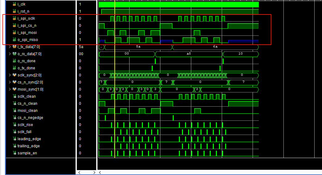
endmodule仿真时序:
【仿真文件】tb_spi_slave.sv
c
`timescale 1ns / 1ps

module tb_spi_slave;

    // =========================================================================
    // 1. 参数配置
    // =========================================================================
    parameter DATA_WIDTH = 8;

    // 修改这里来测试不同的 SPI 模式 (0, 1, 2, 3)
    // Mode 0: CPOL=0, CPHA=0
    // Mode 3: CPOL=1, CPHA=1
    parameter CPOL = 0;
    parameter CPHA = 0;

    parameter CLK_PERIOD = 10;      // 系统时钟 100MHz (10ns)
    parameter SPI_PERIOD = 100;     // SPI时钟 10MHz (100ns) - 确保满足过采样要求

    // =========================================================================
    // 2. 信号声明
    // =========================================================================
    logic                  i_clk;
    logic                  i_rst_n;

    // SPI 物理接口
    logic                  i_spi_sclk;
    logic                  i_spi_cs_n;
    logic                  i_spi_mosi;
    wire                   o_spi_miso; // MISO 是双向/三态信号,使用 wire

    // 用户接口
    logic [DATA_WIDTH-1:0] i_tx_data;
    logic [DATA_WIDTH-1:0] o_rx_data;
    logic                  o_rx_done;
    logic                  o_tx_done;

    // Testbench 内部变量
    logic [DATA_WIDTH-1:0] master_rx_data; // 主机接收到的数据

    // =========================================================================
    // 3. DUT 例化
    // =========================================================================
    spi_slave #(
        .DATA_WIDTH (DATA_WIDTH),
        .CPOL       (CPOL),
        .CPHA       (CPHA)
    ) dut (
        .i_clk      (i_clk),
        .i_rst_n    (i_rst_n),
        .i_spi_sclk (i_spi_sclk),
        .i_spi_cs_n (i_spi_cs_n),
        .i_spi_mosi (i_spi_mosi),
        .o_spi_miso (o_spi_miso),
        .i_tx_data  (i_tx_data),
        .o_rx_data  (o_rx_data),
        .o_rx_done  (o_rx_done),
        .o_tx_done  (o_tx_done)
    );

    // =========================================================================
    // 4. 时钟生成
    // =========================================================================
    initial i_clk = 0;
    always #(CLK_PERIOD/2) i_clk = ~i_clk;

    // =========================================================================
    // 5. 测试主流程
    // =========================================================================
    initial begin
        // --- 初始化 ---
        i_rst_n     = 0;
        i_spi_cs_n  = 1;
        i_spi_mosi  = 0;
        i_tx_data   = 0;
        // SCLK 初始状态取决于 CPOL
        i_spi_sclk  = (CPOL) ? 1'b1 : 1'b0;

        $display("---------------------------------------------------");
        $display("Simulation Start: SPI Mode (CPOL=%0d, CPHA=%0d)", CPOL, CPHA);
        $display("---------------------------------------------------");

        // --- 复位序列 (同步复位) ---
        repeat(5) @(posedge i_clk);
        i_rst_n = 1;
        repeat(5) @(posedge i_clk);

        // --- Test Case 1: 单字节传输 ---
        // 主机发 0xA5, 从机发 0x5A
        $display("[Test 1] Master sends 0xA5, Slave sends 0x5A");

        // 1. 设置从机要发送的数据
        i_tx_data = 8'h5A;

        // 2. 启动主机传输任务 (Master Sending 0xA5)
        spi_master_xfer(8'hA5, master_rx_data);

        // 3. 检查结果
        check_result(8'hA5, o_rx_data, "Slave RX");
        check_result(8'h5A, master_rx_data, "Master RX (MISO)");

        #(CLK_PERIOD * 20); // 插入空闲时间

        // --- Test Case 2: 随机数据传输 ---
        $display("[Test 2] Random Data Transfer");
        begin
            logic [7:0] rand_m_data, rand_s_data;
            rand_m_data = $urandom();
            rand_s_data = $urandom();

            i_tx_data = rand_s_data;
            spi_master_xfer(rand_m_data, master_rx_data);

            check_result(rand_m_data, o_rx_data, "Slave RX");
            check_result(rand_s_data, master_rx_data, "Master RX");
        end

        // --- Test Case 3: 验证 Done 信号 ---
        if (o_rx_done && o_tx_done)
            $display("[Signal Check] Done flags asserted correctly.");
        else
            $error("[Signal Check] Done flags failed to assert!");


        #(CLK_PERIOD * 50);
        $display("---------------------------------------------------");
        $display("Simulation Finished: PASS");
        $finish;
    end

    // =========================================================================
    // 6. 任务:模拟 SPI 主机传输 (Bus Functional Model)
    // =========================================================================
    task spi_master_xfer(
        input  logic [DATA_WIDTH-1:0] data_out, // 主机发送的数据
        output logic [DATA_WIDTH-1:0] data_in   // 主机接收的数据 (MISO)
    );
        integer i;
        logic   leading_edge_val;
        logic   trailing_edge_val;

        // 根据 CPOL 定义边沿电平
        // CPOL=0: Idle=0, Leading=1(Rise), Trailing=0(Fall)
        // CPOL=1: Idle=1, Leading=0(Fall), Trailing=1(Rise)
        leading_edge_val  = (CPOL) ? 1'b0 : 1'b1;
        trailing_edge_val = (CPOL) ? 1'b1 : 1'b0;

        // 1. 拉低 CS_N 开始传输
        i_spi_cs_n = 0;

        // Setup time (CS falling to first clock edge)
        #(SPI_PERIOD/2);

        // 2. 循环传输位
        for (i = DATA_WIDTH-1; i >= 0; i--) begin

            // --- CPHA=0: Data Setup -> Leading Edge (Sample) -> Trailing Edge (Shift) ---
            if (CPHA == 0) begin
                // 在前沿之前建立数据 (MOSI)
                i_spi_mosi = data_out[i];
                #(SPI_PERIOD/2);

                // Leading Edge (Sample by Slave)
                i_spi_sclk = leading_edge_val;

                // 主机在此刻采样 MISO (模拟真实硬件行为,虽然从机是在CS下降沿放数据的)
                data_in[i] = o_spi_miso;

                #(SPI_PERIOD/2);

                // Trailing Edge (Shift by Slave)
                i_spi_sclk = trailing_edge_val;
            end

            // --- CPHA=1: Leading Edge (Shift) -> Trailing Edge (Sample) ---
            else begin
                // Leading Edge (Slave outputs data)
                i_spi_sclk = leading_edge_val;

                // 主机更新 MOSI (在第一个边沿之后)
                i_spi_mosi = data_out[i];

                #(SPI_PERIOD/2);

                // Trailing Edge (Sample by Slave)
                i_spi_sclk = trailing_edge_val;

                // 主机采样 MISO
                data_in[i] = o_spi_miso;

                #(SPI_PERIOD/2);
            end
        end

        // 3. 传输结束
        // Hold time (Last clock edge to CS rising)
        #(SPI_PERIOD/2);

        i_spi_cs_n = 1;
        i_spi_mosi = 0; // Return to 0 (optional)

        // 恢复 SCLK 空闲电平 (其实上面循环结束已经是空闲电平了,这里为了保险)
        i_spi_sclk = (CPOL) ? 1'b1 : 1'b0;

    endtask

    // =========================================================================
    // 7. 辅助任务:结果检查
    // =========================================================================
    task check_result(
        input logic [DATA_WIDTH-1:0] expected,
        input logic [DATA_WIDTH-1:0] actual,
        input string                 desc
    );
        if (expected === actual) begin
            $display("[PASS] %s: Expected 0x%h, Got 0x%h", desc, expected, actual);
        end else begin
            $error("[FAIL] %s: Expected 0x%h, Got 0x%h", desc, expected, actual);
        end
    endtask

endmodule
优点 & 缺点:
SPI 协议因其高效和简单的硬件实现而备受青睐,主要优点包括:
- 通信性能高:
- 全双工通信:SPI 默认支持全双工通信(同时发送和接收数据)。
- 高吞吐量:相比 I²C 或 SMBus,SPI 通常能提供更高的数据传输速率。
- 无速率上限:SPI 协议本身没有定义最大时钟频率,速度主要受限于设备本身和布线物理特性。
- 硬件与协议简单灵活:
- 硬件实现简单:从机(Slave)硬件只需一个移位寄存器,且不需要精密的振荡器(直接使用主机的时钟信号)。
- 无需收发器:与 CAN 总线不同,SPI 不需要专门的收发器芯片。
- 协议灵活:传输不限于 8 位字节,消息的大小、内容和用途可以任意选择。
- 寻址与连接优势:
- 无需复杂寻址:从机不需要像 I²C、GPIB 或 SCSI 那样拥有唯一的地址,而是通过片选信号(SS)进行选择。
- 无总线仲裁:由于是单主设备架构,不存在总线仲裁问题及其相关的故障模式。
- 低功耗:由于电路更少(例如不需要上拉电阻),其功耗通常低于 I²C 或 SMBus。
- 菊花链支持:在菊花链(Daisy chain)配置下,即使连接多个设备也不需要额外的片选信号线。
尽管 SPI 速度快,但它缺乏一些现代通信协议的标准特性,主要缺点如下:
- 引脚占用与物理限制:
- 引脚较多:相比 I²C,SPI 需要更多的 IC 封装引脚(即使是三线变体也是如此)。
- 距离受限:仅适用于短距离通信,传输距离远小于 RS-232、RS-485 或 CAN 总线。
- 多从机扩展性差:如果多个从机需要不同的 SPI 模式(极性/相位),主机会频繁重新初始化,导致访问速度变慢。
- 缺乏标准化:
- 无正式标准:SPI 没有正式的标准化组织制定标准,导致无法验证一致性。
- 变体众多:存在许多不同的变体,这使得不同设备间的支持和兼容变得复杂。
- 缺乏内置协议功能:
- 无硬件流控:从机没有硬件流控机制(但主机可以通过延迟时钟边缘来降低速率)。
- 无应答机制:没有硬件从机应答(ACK),主机可能在向不存在的设备发送数据而并不知情。
- 无错误检查:协议本身不包含数据错误检查机制。
- 不支持热插拔:协议不支持动态添加节点(热插拔)。
- 中断处理:中断功能不在 SPI 协议范围内,必须通过额外的带外信号实现。
总结来说,SPI 非常适合对速率要求高、距离短且硬件简单的场景,但在需要复杂错误处理、长距离传输或极少引脚的应用中,可能不如其他总线协议合适。