1.摘要:
对于这款芯片来说,如果想要更高的频率就需要使用QPI模式,或者SPI QUAD模式。具体详情看前面两篇介绍(基于FPGA的APS6404L-3SQR QSPI PSRAM驱动设计(1))和基于FPGA的APS6404L-3SQR QSPI PSRAM驱动设计(2)。
2.FPGA逻辑设计
为了尽可能的验证芯片功能,QPI模式的状态机我是这样设计的:
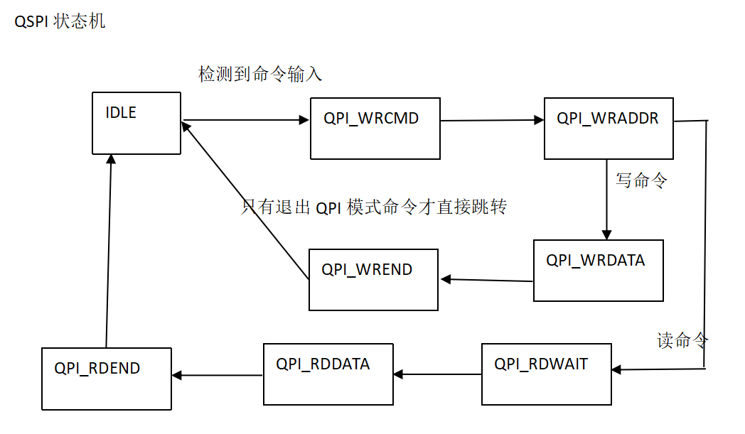
具体代码逻辑如下:
parameter		IDLE		=	5'd0	,
				QPI_WRCMD	=	5'd1	,
				QPI_WRADDR	=	5'd2	,
				QPI_WRDATA	=	5'd3	,
				QPI_WREND	=	5'd4	,
				QPI_RDWAIT	=	5'd5	,
				QPI_RDDATA	=	5'd6	,
				QPI_RDEND	=	5'd7	;

always@(posedge i_clk,posedge i_rst)
begin
	if(i_rst)
		r_qspi_fsm_current	<=	'd0	;
	else
		r_qspi_fsm_current	<=	r_qspi_fsm_next	;
end

always@(*)
begin
	if(i_rst)
		r_qspi_fsm_next	<=	'd0	;
	else begin
		case (r_qspi_fsm_current)
			IDLE		:
				if (w_user_active)
					r_qspi_fsm_next	<=	QPI_WRCMD	;
				else
					r_qspi_fsm_next	<=	IDLE	;
			QPI_WRCMD		:
				if (r_cnt == 'd1 && r_qpi_cnt)
					if (i_exit_qpi_mode)	//退出QPI模式if (i_fsm_current == 'd10)
						r_qspi_fsm_next	<=	QPI_WREND	;
					else
						r_qspi_fsm_next	<=	QPI_WRADDR	;
				else
					r_qspi_fsm_next	<=	QPI_WRCMD		;
			QPI_WRADDR	:
				if (i_qspi_wren && r_cnt == 'd5 && r_qpi_cnt)
					r_qspi_fsm_next	<=	QPI_WRDATA	;
				else if (i_qspi_rden && r_cnt == 'd5 && r_qpi_cnt)
					r_qspi_fsm_next <= QPI_RDWAIT;
				else
					r_qspi_fsm_next	<=	QPI_WRADDR	;
			QPI_WRDATA	:
				if (i_user_data_val && r_qpi_cnt && (r_wrbyte_cnt == i_write_length))
					r_qspi_fsm_next	<=	QPI_WREND	;
				else
					r_qspi_fsm_next	<=	QPI_WRDATA	;
			QPI_WREND	:
				r_qspi_fsm_next	<=	IDLE	;
			QPI_RDWAIT	:
				if (r_cnt == 'd5 && r_qpi_cnt)
					r_qspi_fsm_next	<=	QPI_RDDATA	;
				else
					r_qspi_fsm_next	<=	QPI_RDWAIT	;
			QPI_RDDATA	:
				if (ro_user_read_valid  & (r_rdbyte_cnt == i_read_length))
					r_qspi_fsm_next	<=	QPI_RDEND	;
				else
					r_qspi_fsm_next	<=	QPI_RDDATA	;
			QPI_RDEND	:
				r_qspi_fsm_next	<=	IDLE	;
			default		:
				r_qspi_fsm_next	<=	IDLE	;
		endcase
	end
end
2.1、IDLE状态
在初始状态的跳转和SPI一样,这要此模块准备就绪(o_user_ready为高)且有命令输入即跳出初始状态到达写命令状态。

2.2、QPI_WRCMD状态
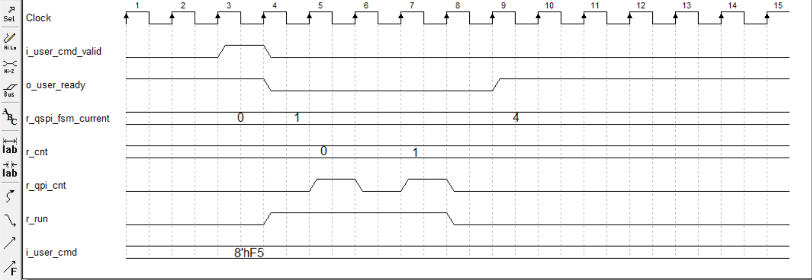
同SPI模块类似,使用r_cnt 和 r_qpi_cnt作为标志状态。同时,既然已经使用了QPI模块那说明在SPI模块肯定已经配置了进入QPI模式,所以在QPI模块除了读写可能还需要一个退出QPI模式的指令,当输入此指令时不需要地址和数据。8bit命令输出完就跳到SPI模式了。如下图所示我这里是以退出QPI模式画的时序图,读写命令的话则跳到写地址状态(QPI_WRADDR):
对于写命令,在(cmd_flag & r_qpi_cnt)锁存下,将命令信号i_user_cmd复制给QPI的四根数据线具体代码为:
	end else if (cmd_flag & r_qpi_cnt) begin
		rio_qspi_mosi0	<=	i_user_cmd[(2-r_cnt)*4 - 4];//8
		rio_qspi_mosi1	<=	i_user_cmd[(2-r_cnt)*4 - 3];//7
		rio_qspi_mosi2	<=	i_user_cmd[(2-r_cnt)*4 - 2];//6
		rio_qspi_mosi3	<=	i_user_cmd[(2-r_cnt)*4 - 1];//5
2.3、QPI_WRADDR状态
地址没什么好说的和写命令几乎是一模一样,命令是8bit,地址是24bit/4 = 6个clk,所以r_cnt技术到5即可。然后根据是写命令还是读命令分别跳转到QPI_WRDATA(写数据)或者QPI_RDWAIT(读等待)状态。具体时序图如下:

对于写地址,在(addr_flag & r_qpi_cnt)锁存下,将命令信号i_user_wr_addr复制给QPI的四根数据线具体代码为:
	end	else if (addr_flag & r_qpi_cnt)	begin
		rio_qspi_mosi0	<=	i_user_wr_addr[(6-r_cnt)*4 - 4];//4
		rio_qspi_mosi1	<=	i_user_wr_addr[(6-r_cnt)*4 - 3];//5
		rio_qspi_mosi2	<=	i_user_wr_addr[(6-r_cnt)*4 - 2];//6
		rio_qspi_mosi3	<=	i_user_wr_addr[(6-r_cnt)*4 - 1];//7
2.4、QPI_WRDATA状态
写数据状态跳转也是换汤不换药,一个样子。无非就是多加一个写计数器(r_wrbyte_cnt),当写计数器到了写突发长度时候跳出写数据状态。
always@(posedge i_clk,posedge i_rst)
begin
	if(i_rst)
		r_wrbyte_cnt	<=	'd0	;
	else if (i_user_data_val && r_qpi_cnt && (r_wrbyte_cnt == i_write_length))
		r_wrbyte_cnt	<=	'd0	;
	else if (i_user_data_val && r_qpi_cnt)
		r_wrbyte_cnt	<= r_wrbyte_cnt + 'd1	;
end 
同样对于数据,由于是一个clk传输4bit,且数据是一直传输,所以我们对r_qpi_cnt在进行二分频处理得出r_wrfifo_flag信号,在根据r_wrfifo_flag的上升沿和下降沿进行不同位的写入:
always@(posedge i_clk,posedge i_rst)
begin
	if(i_rst)
		r_wrfifo_flag	<=	'd0	;
	else if (r_qpi_cnt)
		r_wrfifo_flag	<= ~r_wrfifo_flag	;
	else
		r_wrfifo_flag	<=	r_wrfifo_flag	;
end

	end else if (wr_data_flag & r_qpi_cnt)	begin
		if (!r_wrfifo_flag)	begin
			rio_qspi_mosi0	<=	i_user_data[P_DATA_WIDTH - 4];//4
			rio_qspi_mosi1	<=	i_user_data[P_DATA_WIDTH - 3];//5
			rio_qspi_mosi2	<=	i_user_data[P_DATA_WIDTH - 2];//6
			rio_qspi_mosi3	<=	i_user_data[P_DATA_WIDTH - 1];//7
		end else begin
			rio_qspi_mosi0	<=	i_user_data[P_DATA_WIDTH - 8];//4
			rio_qspi_mosi1	<=	i_user_data[P_DATA_WIDTH - 7];//5
			rio_qspi_mosi2	<=	i_user_data[P_DATA_WIDTH - 6];//6
			rio_qspi_mosi3	<=	i_user_data[P_DATA_WIDTH - 5];//7
		end
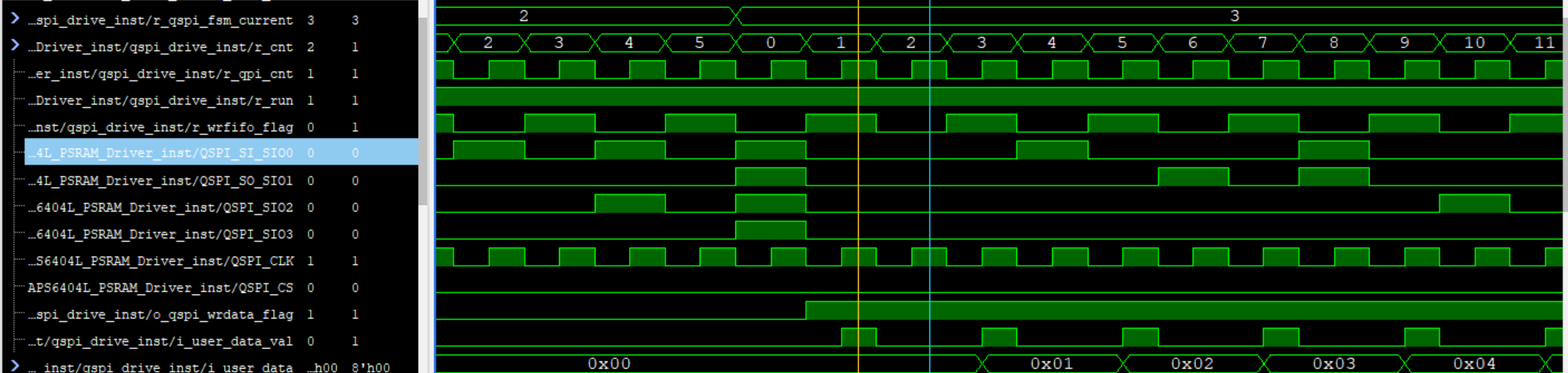
具体如下图所示:黄色线是第一个clk写入0000,蓝色线是第二个clk写入0000,第一个数据即为0000_0000。同理第二个数据为0000_0001.。。。。。
2.5、QPI_RDDATA状态
读等待状态就不记录了,一个样子。到读数据状态时需要接受来自PSRAM的读数据,和写数据一样,反过来即可,加一个读计数器,读到突发长度跳出状态。
always@(posedge i_clk,posedge i_rst)
begin
	if(i_rst)
		r_rdbyte_cnt <= 'd0;
	else if (ro_user_read_valid & (r_rdbyte_cnt == i_read_length))
		r_rdbyte_cnt <= 'd0;
	else if (ro_user_read_valid)
		r_rdbyte_cnt <= r_rdbyte_cnt + 'd1;
	else
		r_rdbyte_cnt <= r_rdbyte_cnt;
end

always@(negedge o_spi_clk,posedge i_rst)
begin
	if(i_rst)
		ro_user_read_data <= 'd0;
	else if (r_rd_data_flag[1] & r_qpi_cnt)	begin
		if (r_wrfifo_flag)	begin
			ro_user_read_data[P_DATA_WIDTH - 1] <= i_qspi_sio3;
			ro_user_read_data[P_DATA_WIDTH - 2] <= i_qspi_sio2;
			ro_user_read_data[P_DATA_WIDTH - 3] <= i_qspi_sio1;
			ro_user_read_data[P_DATA_WIDTH - 4] <= i_qspi_sio0;
		end  else begin
			ro_user_read_data[P_DATA_WIDTH - 5] <= i_qspi_sio3;
			ro_user_read_data[P_DATA_WIDTH - 6] <= i_qspi_sio2;
			ro_user_read_data[P_DATA_WIDTH - 7] <= i_qspi_sio1;
			ro_user_read_data[P_DATA_WIDTH - 8] <= i_qspi_sio0;
		end
	end else
		ro_user_read_data <= ro_user_read_data;
end
至于读出数据标志,也一样和读数据的条件一样。
always@(posedge i_clk,posedge i_rst)
begin
	if(i_rst)
		ro_user_read_valid <= 'd0;
	else if (r_rd_data_flag[1] & r_qpi_cnt & !r_wrfifo_flag)
		ro_user_read_valid <= 'd1;
	else
		ro_user_read_valid <= 'd0;
end
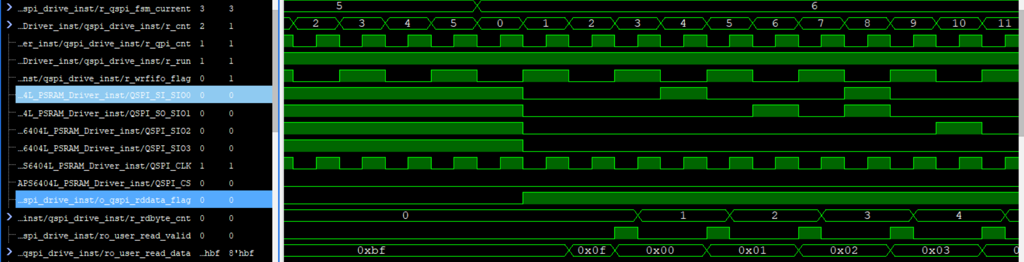
具体结果如下图所示,读出数据为00,01,02.。。。。。。。。。。。。。。:
3、顶层端口
qspi_drive#(
    parameter               	P_DATA_WIDTH        	= 8 ,
							P_ADDR_WIDTH		= 24,
							P_READ_DATA_WIDTH   	= 8 ,
							P_CPOL              	= 0 ,
							P_CPHL              	= 0
)(
	input	wire					i_clk               ,
	input	wire					i_rst               ,

	output	wire					o_spi_clk           ,
	output	wire					o_spi_cs            ,

	/*synthesis PAP_MARK_DEBUG="1"*/input	wire					i_qspi_sio0		,
	/*synthesis PAP_MARK_DEBUG="1"*/input 	wire					i_qspi_sio1		,
	/*synthesis PAP_MARK_DEBUG="1"*/input	wire					i_qspi_sio2		,
	/*synthesis PAP_MARK_DEBUG="1"*/input 	wire					i_qspi_sio3		,
	output	wire					o_qspi_sio0		,
	output	wire					o_qspi_sio1		,
	output	wire					o_qspi_sio2		,
	output	wire					o_qspi_sio3		,
	/*synthesis PAP_MARK_DEBUG="1"*/output 	wire					o_qspi_cmd_flag	,
	/*synthesis PAP_MARK_DEBUG="1"*/output 	wire					o_qspi_addr_flag	,
	/*synthesis PAP_MARK_DEBUG="1"*/output 	wire					o_qspi_wrdata_flag	,
	/*synthesis PAP_MARK_DEBUG="1"*/output 	wire					o_qspi_rddata_flag	,

	input	wire					i_fifo_full	,
	input	wire					i_qspi_wren		,
	input	wire					i_qspi_rden		,
	input	wire	[7:0]			i_write_length	,
	input	wire	[7:0]			i_read_length	,
	input	wire					i_exit_qpi_mode	,
	output 	wire					o_wr_requset	,

	/*synthesis PAP_MARK_DEBUG="1"*/input	wire	[23:0]			i_user_wr_addr	,
	/*synthesis PAP_MARK_DEBUG="1"*/input	wire	[7 :0]   		i_user_data         ,
	/*synthesis PAP_MARK_DEBUG="1"*/input	wire					i_user_data_val	,
	/*synthesis PAP_MARK_DEBUG="1"*/input	wire	[7 :0]   		i_user_cmd        ,
	/*synthesis PAP_MARK_DEBUG="1"*/input	wire					i_user_cmd_valid       ,
	output	wire					o_user_ready        ,

	output	wire	[7:0]   			o_user_read_data    ,
	output	wire                        o_user_read_valid
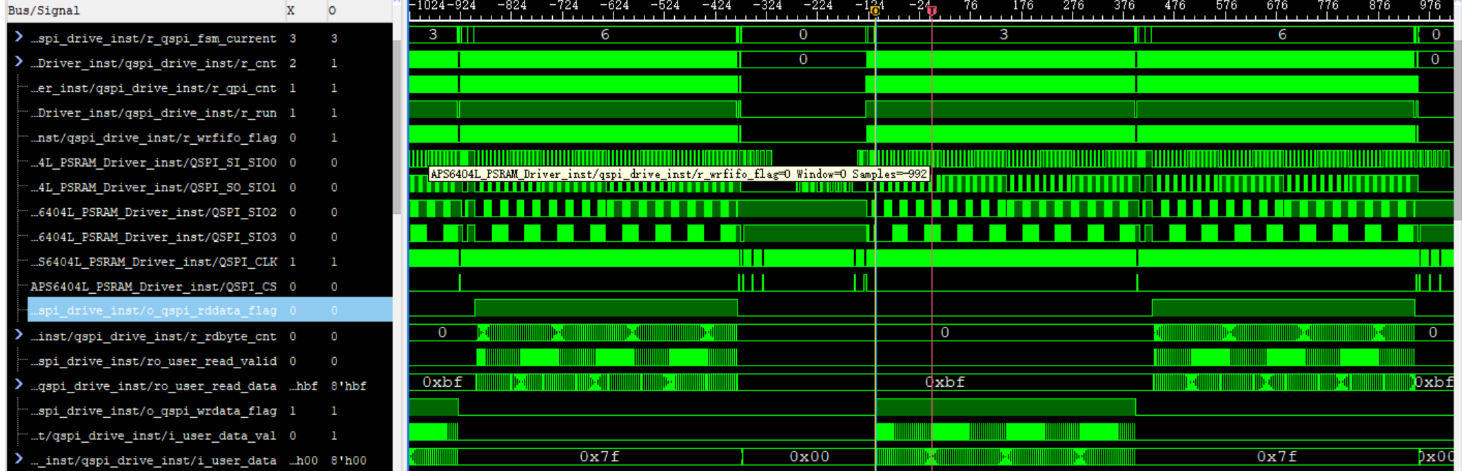
);
循环读写debug,信号抓取结果: